HAL Id: hal-01053188
https://hal.archives-ouvertes.fr/hal-01053188
Submitted on 29 Jul 2014
HAL is a multi-disciplinary open access
archive for the deposit and dissemination of
sci-entific research documents, whether they are
pub-lished or not. The documents may come from
teaching and research institutions in France or
abroad, or from public or private research centers.
L’archive ouverte pluridisciplinaire HAL, est
destinée au dépôt et à la diffusion de documents
scientifiques de niveau recherche, publiés ou non,
émanant des établissements d’enseignement et de
recherche français ou étrangers, des laboratoires
publics ou privés.
Challenges in probing space charge at sub-micrometer
scale
G. Teyssedre, Christina Villeneuve-Faure, Patrick Pons, Laurent Boudou, K
Makasheva, Bernard Despax
To cite this version:
G. Teyssedre, Christina Villeneuve-Faure, Patrick Pons, Laurent Boudou, K Makasheva, et al..
Chal-lenges in probing space charge at sub-micrometer scale. Electrical Insulation and Dielectric Phenomena
(CEIDP), Oct 2012, Montreal, Canada. 5 p. �hal-01053188�
Challenges in probing space charge
at sub-micrometer scale
G. Teyssedre
1,2*, C. Villeneuve
1, P. Pons
3,4, L. Boudou
1, K. Makasheva
1,2and B. Despax
1,21
Université de Toulouse; UPS, INPT; LAPLACE (Laboratoire Plasma et Conversion d’Energie); 118 route de Narbonne, F-31062 Toulouse cedex 9, France
2
CNRS; LAPLACE; F-31071 Toulouse, France 3
CNRS,LAAS, 7 avenue Colonel Roche; F-31400 Toulouse, France 4
Univ de Toulouse, LAAS, F-31400 Toulouse, France *Corresponding author: [email protected]
Abstract- An overview of current limitations and challenges
with techniques, based either on acoustic or thermal perturbation, providing charge density profiles within insulations, is presented. Even though the resolution could be somewhat improved, technical limitations readily appear, related to the bandwidth of signals to be detected and to the sensitivity. Instead, our purpose here is to exploit near field techniques derived from AFM – Atomic Force Microscopy-. A booming of the availability and versatility of equipments is observed today. A spatial resolution of some tens of nanometers is accessible for charge detection which therefore let's the possibility to investigate selectively regions with specific properties. The measuring conditions and operating mode for both the sensitivity and spatial resolution of the techniques are addressed and examples of application of these techniques to charge detection in insulating materials are presented.
I. INTRODUCTION
One of the common properties of all solid dielectrics, being used as electrical insulating parts or as energy storage components, and whatever the size of devices (application related to electrotechnics, power electronics, microsystems, microelectronics, etc.) is their propensity to accumulate electrical charges beyond a critical electric field. Whatever the application field considered, it is actually necessary to implement diagnostic means of the charging state that are fitting to the stresses, environment, nature and geometry of materials in conditions that are representative of their real conditions in the application. Along this aim, a wealth of techniques has been developed over the last decades enabling probing charge build for dielectric thickness ranging from several cm to some tens of µm. The lower scale limit actually represents a serious limitation as many dielectrics are used in the sub-micron range of thickness. Without being exhaustive, one can quote here wiring of motors (typically 20-40µm thickness), insulation/passivation in power electronics (some µm), protective insulations in outer parts of spacecraft (some tens of µm), integrated and miniaturized devices: actuators, MEMS, lab-on-a-chip, dosimeters, passivation layers, with µm or sub-µm scale; microelectronics: SiO2 gates, non-volatile memory devices (nm scale); photovoltaic devices: 3rd generation solar cells (nm scale).
Besides, identification and understanding of physical phenomena at play require implementing techniques to
provide information at the scale where physical processes occur, e.g. at interfaces, whether formed by the limits of the solid insulation (metal-dielectric interface, air/dielectric) or at the borders of domains of different nature, i.e. at dielectric/dielectric interfaces. Triboelectrification, flow electrification phenomena, corona charging are examples of processes analyzed so far only as surface charging phenomena due to a lack of in-depth information. In the dielectric bulk, at the nanometer scale, charge storage is controlled by atoms or atom groups liable to introduce impurity levels owing to their specific electronic properties. At the meso-scale of some tens or hundreds of nm, it is crystalline, supermolecular architecture that constitutes specific domain in respect to the amorphous phase. It is therefore at these different scales that electronic properties of insulating materials must be probed as a route to feed models describing transport properties at the macroscale with the intention to reveal the physical phenomenon at play.
In this communication, we first briefly recall the present performances obtained by techniques with in-depth resolution for charge density profile measurements. We also comment on the technical limitations in further improvement of the resolution. As improving the resolution beyond some tenths of µm does actually represent a huge challenge, strategies consisting in applying near-field techniques derived from atomic force microscopy –AFM- are heavily developing. The principles of such techniques and the options for detection of electrical charges based on electrostatic force interactions between the AFM tip and the dielectric surface are described. Finally, examples of results obtained by probing silicon oxy-nitride layers are shown.
II. TECHNIQUES WITH IN-DEPTH RESOLUTION
OF CHARGES:SPATIAL RESOLUTION
The ultimate spatial resolution of conventional space charge measurement techniques (based on acoustic or thermal principles) is often evaluated considering the shape of the perturbation being applied [1, 2]. With this criterion, the spatial resolution is by principle quite different weather one considers wave propagation techniques (either pressure-wave –PIPWP– or pulsed electroacoustic –PEA– methods) or thermal methods (Laser Induced Modulation Method –LIMM– or Thermal Pulse –TP–). Ideally, the definition
should correspond to the shortest distance between 2 plans of charges that can be distinguished. An excitation-related criterion consists in considering the shortest distance over which the perturbation varies from 10 to 90% of its amplitude [3]. For wave propagation method (with symmetrical pulse), the resolution is of the form:
max 2 R f
,
(1)where is the risetime of the excitation pulse and is the sound velocity; fmax is the required bandwidth of the detection
system. For reaching a resolution of 100nm, considering a sound velocity of 2000m/s typical of polymers, (1) leads to a bandwidth of 10GHz.
For thermal methods the resolution depends on the diffusivity (D) of heat and on time (t):
max 2.35 2.35 2 D R Dt f . (2)
For 100nm resolution (at 50% amplitude) and a diffusivity of 10-7m²/s (of polymers), fmax is of the order of 10MHz.
As depicted in Fig. 1, the in-depth resolution is not dependent on the position in the sample for pressure wave methods. Conversely, the resolution decreases with the penetration of the heat front in the bulk with thermal methods. For this reason, although better resolution has been achieved so far for thermal methods, it must be said that it is only close to the surface on which the heat flux is provided.
Fig. 1. Spatial resolution in charge measurement vs. depth in the sample for pressure wave (left) and thermal methods (right). From [3].
The actual resolution is impeded by factors other than the shape of the perturbation, some of them being inherent to the shape/nature of test materials, like attenuation and dispersion of acoustic waves by the sample, which may impose to work on thin dielectrics to maintain a targeted resolution. The geometry and electromechanical losses of the piezoelectric sensor (PEA method) and the deconvolution procedure [4] are influential in the resolution achieved. Impedance matching between voltage pulse and sample capacitance becomes an issue when increasing bandwidth. Thermal methods need an accurate and simultaneous measurement of surface temperature profile for accurate deconvolution. Improving resolution means increasing bandwidth, which goes with a loss in amplifier gain and with impedance mismatch issues. Also the perturbation energy decreases as the frequency increases meaning that sensitivity and signal-to-noise ratio will provide new challenges.
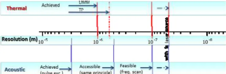
Fig. 2 represents current achievements of various techniques (LIMM and TP for thermal methods, and PEA). A resolution of 0.5µm has been reported for TP, very close to the sample surface [5]. In case of PEA, a resolution of 3-4µm has been achieved [6]. Incremental improvement of the PEA method with the current principle could perhaps bring the resolution to 1µm or slightly beyond, but a switch to frequency scan for the excitation would be preferable for impedance mismatch issues. The LIMM method could also be improved through appropriate amplifier is settled and surface temperature can be monitored. In both cases, with the bandwidth figures given above, it is difficult to envisage a resolution better than 100nm.
Dagher et al. [3] reconsidered the different techniques using perturbation based on femtosecond laser pulses, providing thermal pulse (TP) excitation or thermally-induced elastic waves (PIPWP) or ps field pulses via a semiconducting crystal (PEA). The detection side would consist in electromagnetic field detection through an electro-optical crystal (TP and PIPWP) or surface displacement detection by interferometry (PEA). Though the specifications have been settled targeting a resolution of 60nm in SiO2, the development of such instruments remains extremely challenging.
Fig. 2. Sketch of achieved resolution, and hypothetical improvements that could be brought for thermal and acoustic principles.
III.INPUT OF SCANNING PROBE MICROSCOPY
Scanning probe microscopy –SPM– has emerged and spread in a family of techniques since the development of scanning tunnelling microscopy, in 1982, which was limited to topography investigation of conductive materials at the nanometer scale [7]. AFM has brought an important progress as it could be applied to either conductive or insulating materials to obtain images at atomic scale. The contrast is essentially based on the gradient of interaction forces between a tip and the surface to be probed. A wealth of techniques has appeared based on the scanning of forces of different natures (magnetic, mechanical, chemical, etc...). As the influence length of different forces depends on their nature, different images can be obtained as a function of the scanning distance from the surface. Table 1 provides with order of magnitude of forces probed by Scanning Force Microscopy –SFM– and on their influence length. The detection of electrostatic forces has naturally emerged as a way to carry out imaging based on surface potential contrast, induced e.g. by electrical charges stored on the surface. EFM (Electrostatic Force Microscopy)
and KPFM (Kelvin Probe Force Microscopy) are two of the variants developed for that purpose [8, 9].
TABLE 1.ORDER OF MAGNITUDE AND INFLUENCE LENGTH OF FORCES BETWEEN AFM TIP AND SAMPLE SURFACE MEASURED BY SFM
Origin Nature Influence
length
Force strength
Electron cloud (Pauli) Repulsive Very short (0-1nm) 1nN
Van Der Waals Attractive Short
(0-10nm) 5nN
Capillarity (strong in air) Attractive a few 100nN
Molecular Adhesion Attractive Middle (0-50nm)
Electrostatic (surface charges) Attractive/
Repulsive Long (0-100nm) 1nN to some 10nN Magnetostatic (magnetic materials) Attractive/ Repulsive
EFM and KPFM techniques differ by the way electrostatic forces are measured. Only a brief description is given here [10]. In EFM, the frequency variations m of the tip
vibration due to static electrostatic forces FDC are measured:
2 2 1 S DC V dz dC F and ( ) 2 1 0 o DC m m z dz dF k
, (3)where Vs is the surface potential difference and C the tip-surface capacitance. In KPFM, an ac voltage is applied to the tip that provides a dynamic force of the form:
) sin( ) ( ) ( V V V t dz dC F
S FB AC
(4)The dynamic force is cancelled out by applying a feedback loop VFB on the potential of the tip. As F() depends on the 1st
derivative of capacitance whereas m depends on the 2nd
derivative, KFPM is more sensitive to parasitic capacitance. However, the surface potential is obtained directly, and there is no perturbation due to influence charge on the tip.
In our context, the objective is not only to record images (and optimize spatial resolution) of the surface based on electrostatic properties contrast. A more important goal is to bring the technique to quantitative and reliable surface charge density measurement. So, the relative merit of the techniques has to be evaluated based on that objective.
An important feature of these techniques is that only lateral resolution is achieved with no in-depth resolution. This represents a serious limitations compared to techniques presented in section I. However, strategies have been implemented for obtaining field profiles by EFM technique along the inter-electrode distance by using imbedded electrodes [11] with resolution well beyond the µm scale. This has been applied to semiconducting materials, however there is no apparent issue preventing its extension to insulating materials.
IV. KPFM ONa-SiOxNy:HLAYERS WITH DIFFERENT
CONDUCTIVITIES
Pulsed plasma-enhanced chemical vapor deposition (PPECVD) is used as deposition technique to elaborate the layers [12]. Thin amorphous silicon oxy-nitride layers (a-SiOxNy:H, x < 2, y < 1) are deposited on Au/Ti-metallized Si wafers in the plasma of radiofrequency (f = 13.56 MHz) capacitively coupled discharge (P = 5 W, p = 65 Pa), modulated with square pulses of period T = 400 ms and pulse
width of 100 ms. The gas mixture contains SiH4, N2O and He (40%). The ratio = N2O/SiH4 allows adjusting the silicon content in the film. The substrate temperature is kept to 300°C during deposition. Layers with three different -values (100, 10 and 5) have been used for the current study. = 100 implies a layer with composition close to a SiO2-layer. When decreasing the -value the Si-concentration in the layer increases, hence its conductivity.
Spectroscopic ellipsometry has been used to record the spectra aiming at a structural characterization of the layers. Forouhi-Bloomer approximation [13] is applied for the spectra processing to find out thicknesses and optical properties of the layers. The optical band gap is deduced from Tauc’s law. The results are summarized in Table 2.
One can notice that the γ = 100 a-SiOxNy:H-layer has a refractive index close to that of fused silica layer (n = 1.457). The obtained quite high optical band gap of γ = 100-layer describes it is as a good dielectric layer. Decreasing the -value leads to deposition of layers with higher refractive indexes and lower optical band gaps mainly due to a higher Si-content, hence different Si-environment in the layer. The structural characterization of γ = 5 layer shows that this layer can represent semi-conducting properties (Eg is only 2.8 eV).
TABLE 2.THICKNESSES, OPTICAL PROPERTIES AND LOW FIELD RESISTIVITY OF a-SiOxNy:H LAYERS a-SiOxNy:H layer Thickness [nm] Refractive index- n (at =632.8nm) Optical band gap Eg [eV] Resistivity [.m] γ = 100 116.6 0.7 1.49 5.03 2.2 1015 γ = 10 207.0 6.3 1.55 4.2 4.9 1014 γ = 5 165.7 4.6 1.61 2.8 3.8 1014
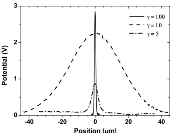
KPFM measurements are carried after charging the material by an AFM tip with voltages up to 25V for times from 10s up to 10min. Results for 25V are shown in the following. Note that the field is relatively high (order 100-200kV/mm), compared to that obtained for conductivity values (3-60kV/mm) given in Table 2 [12]. To improve accuracy and reproducibility, some parameters need to be controlled: (i) humidity is the most critical one [14]. Measurement are done under N2 flow and Force Distance Curve is used to follow adhesion due to water adsorbed on sample surface; and (ii) contact force which is kept small to ensure tip integrity. Injected charge is punctual, so only a cross-section of potential map is shown. Three parameters are extracted from this profile: maximum potential Vm, full width at half maximum,
Wh and the integrated intensity Is along the profile.
KFM measurement of surface potential emphasizes different behaviour for each layer in terms of charges injection and decay. Indeed, resulting potential profiles of Fig. 3 exhibit strong differences between different layers. For γ=100 and γ=5 charges are stored close to the injection contact point (Wh=0.9
and 4.6µm, respectively) whereas γ=10 layer exhibits strong lateral charges spreading (Wh=37µm). For γ=100 and γ=5
layers, a saturation of injected charge is observed with increasing charging time (results not shown). In γ=10 layer, the charge spot broadens and grows without saturation effect with injection time.
-40 -20 0 20 40 0 1 2 3 Position (µm) Potential (V)
Fig. 3. Potential profiles induced by charge injection at 25V during 2min for different layers.
Fig. 4 shows the change in time of parameters of the potential profiles during release of the charges. Again, marked contrasts are observed. For γ=100 layer, peak intensity Vm and
area Is remain constant in time and no broadening is observed:
charges remain trapped. For γ=10, a decrease of both Vm and Is
is observed, meaning that drift along the surface (reflected by significant peak broadening) and through the bulk of the dielectric (reflected by changes in Is) occur concomitantly.
Finally, for =5, the peak broadens at short time and then stays unchanged. The area and the intensity of the peak follow a parallel behaviour. Hence, charges would be dominantly evacuated through the dielectric bulk to the ground.
0 200 400 600 800 0.0 0.2 0.4 0.6 0.8 1.0 = 100; = 10; = 5 Normal ized Magni tude Vm n and area Isn
Time after injection (s)
1 2 3 Pe a k w id th W h /W ho
Fig. 4. Evolution of the normalized maximum Vmn (solid symbols), the
normalized integrated intensity Isn (open symbols) and normalized peak width
(grey) after charge injection for different layers γ = 100 (squares), γ = 10 (triangles) and γ = 5 (circles). Bias injection of 25V during 2min.
Results for the different materials can be understood as follows. For γ =100, owing to the good insulation properties, it can be supposed that charges get trapped close to the injecting electrode and form a screening field that prevent further charge injection. For =5, a significant leakage of charges to the ground during charging occurs. The saturation effect in charging corresponds to the building-up of equilibrium between charging and leakage. The case of =10 is much more appealing. A significant charge cloud expansion along the
surface is observed both during charging and discharging. The conductivity value obtained in the linear regime is close to that for =5, but the trend can be different for the high field range. Anyway, conductivity alone cannot explain the features (spreading of charges over several tens of µm with a layer thickness of 200nm). A possible effect is the formation of deep traps, induced by high electric field under AFM tip. Such traps would limit charge conduction in the volume and would promote occupation of lateral shallow traps. More work needs to be done for further understanding the marked contrasts observed by KPFM on the dielectric properties of these layers.
V. CONCLUSION
A technical limit in spatial resolution of charge distribution measurement methods is being reached, preventing their use in µm scale dielectric thicknesses. The increasing needs for characterizing relatively thin film dielectrics can be covered by electrostatic techniques based on scanning force microscopy which come to a mature stage even though developments are on the way. The examples shown here have not touched the spatial resolution of the techniques (≈50nm) because of the nature of materials that tend to spread charges. Promising results are obtained on these a-SiOxNy:H layers.
REFERENCES
[1] R.J. Fleming, "Space charge profile measurement techniques: recent advances and future directions", IEEE Trans. Dielectr. Electr. Insul. 12, 967, 2005
[2] S. Holé, "Resolution of direct space charge distribution measurement methods", IEEE Trans. Dielectr. Electr. Insul. 15, 861, 2008
[3] G. Dagher S. Holé, and J. Lewiner, "A preliminary study of space charge distribution measurements at nanometer spatial resolution", IEEE Trans. Dielectr. Electr. Insul. 13, 1036, 2006
[4] M Arnaout, F Baudoin, L Berquez, and D Payan, "Study of signal treatment for a pulsed electro-acoustic measurement cell: a way of improving the transfer matrix condition number", J. Phys. D: Appl. Phys. 44, 405403, 2011
[5] A. Mellinger et al., "Three-dimensional mapping of polarization profiles with thermal pulses", Appl. Phys. Letts. 86, 082903, 2005
[6] T. Maeno and K. Fukunaga, "High-resolution PEA charge distribution
measurement system", IEEETrans. Dielectr. Electr. Insul. 3, 754, 1996
[7] G. Binnig and C. F. Quate, "Atomic Force Microscope", Phys. Rev. Lett. 56, 930-933, 1986.
[8] G.C. Stevens and P. Baird, "Nano- and meso-measurement methods in the study of dielectrics", IEEE Trans. Dielectr. Electr. Insul. 12, 979, 2005 [9] C.A. Rezende, R.F. Gouveia, M.A. da Silva, and F. Galembeck,
"Detection of charge distributions in insulator surfaces", J. Phys.: Condens. Matter 21, 263002, 2009
[10] T. Mélin, M. Zdrojek, and D. Brunel, in Scanning Probe Microscopy in
Nanoscience and Nanotechnology, Part 1. pp. 89-128, Springer-Verlag,
Berlin, 2010
[11] W.R. Silveira and J.A. Marohn, "Microscopic view of charge injection in an organic semiconductor", Phys. Rev. Lett. 93, 116104, 2004 [12] K. Makasheva, B. Despax, L. Boudou, and G. Teyssedre, "Dielectric
layers for RF-MEMS switches: design and study of appropriate structures preventing electrostatic charging", IEEE Trans. Dielectr. Electr. Insul. 2012, in press
[13] A. R. Forouhi and I. Bloomer, "Optical dispersion relations for amorphous semiconductors and amorphous dielectrics", Phys. Rev. B 34, 7018, 1986
[14] U. Zaghloul et al., "On the influence of environment gases, relative humidity and gas purification on dielectric charging/discharging processes in electrostatically driven MEMS/NEMS devices", Nanotechnology 22, 035705, 2011