This is an author-deposited version published in:
http://oatao.univ-toulouse.fr/
Eprints ID: 8363
To link to this article: DOI: 10.1109/TNS.2012.2193671
URL:
http://dx.doi.org/10.1109/TNS.2012.2193671
To cite this version:
Place, Sébastien and Carrere, Jean-Pierre and
Allegret, Stephane and Magnan, Pierre and Goiffon, Vincent and Roy,
François Radiation Effects on CMOS Image Sensors With Sub-2 µm
Pinned Photodiodes. (2012) IEEE Transactions on Nuclear Science, vol.
59 (n° 4). pp. 909-917. ISSN 0018-9499
O
pen
A
rchive
T
oulouse
A
rchive
O
uverte (
OATAO
)
OATAO is an open access repository that collects the work of Toulouse researchers and
makes it freely available over the web where possible.
Any correspondence concerning this service should be sent to the repository
administrator:
staff-oatao@inp-toulouse.fr
Radiation Effects on CMOS Image Sensors With
Sub-2
Pinned Photodiodes
S. Place, J.-P. Carrere, S. Allegret, P. Magnan, V. Goiffon, and F. Roy
Abstract—CMOS image sensor hardness under irradiation is a key parameter for application fields such as space or medical. In this paper, four commercial sensors featuring different technolog-ical characteristics (pitch, isolation or buried oxide) have been ir-radiated with source. Based on dark current and temporal noise analysis, we develop and propose a phenomenological model to explain pixel performance degradation.
Index Terms—Activation energy, APS, CMOS 4T image sensor, dark current, irradiation, pinned photodiode, temporal noise.
I. INTRODUCTION
T
HE recent evolution of mobile phone market has estab-lished CMOS Image Sensors (CIS) as the new standard for such imaging applications. These devices actually do offer the best scaling capability for pixels. Recent achievements close to micron sizes allow getting low-cost image sensors up to 10 Mega-pixels (Mpix). In order to maintain the signal-to-noise ratio while scaling the pixel size, specific care was taken to min-imize noise sources. One of the most efficient ways is to use a 4T CMOS pinned photodiode pixel [1]–[4].The use of these commercial image sensors extends in some harsh environments applications, especially for the medical, sci-entific or spatial imaging domains [5]. This involves new re-quirements, including that the CIS should become radiation tol-erant. Several studies have already been dedicated to the ion-izing dose induced degradation in 3T CMOS pixel ([6]–[9]), but very few are related to commercial 4T CMOS pixels with pinned photodiodes [10]–[12].
In this paper we report on the degradation induced by gamma rays on some small-pitch 4T CMOS image sensors, down to 1.4 pixel pitch. The impact of different technolog-ical features such as Trench Isolation (TI), buried oxide (BOX) and multiple doped lateral interfaces is investigated. The pixel degradation will be first characterized by measuring the pixel dark current degradation with Total Ionizing Dose (TID). The
S. Place is with the ST Microelectronics, Crolles 38926, France, and also with Université de Toulouse, ISAE, Toulouse 31055, France (e-mail: sebastien. place@st.com).
J.-P. Carrere, S. Allegret, and F. Roy are with ST Microelectronics, Crolles 38926, France (e-mail: jean-pierre.carrere@st.com; stephane.allegret@st.com; francois.roy@st.com).
P. Magnan and V. Goiffon are with the Université de Toulouse, ISAE, Toulouse 31055, France (e-mail: vincent.goiffon@isae.fr; pierre.magnan@isae. fr).
Fig. 1. Schematic representation of 4T CMOS pixel.
evolution of the dark current activation energy will also be shown to complete the discussion about the pixel degradation scheme. Finally, the pixel temporal noise evolution with TID will also be presented and discussed, assuming that the pixel dark current and the temporal noise are the major contributors of the pixel noise floor.
II. EXPERIMENTALDETAILS
Most of the CMOS image sensors are on the so-called Ac-tive Pixel Sensor (APS) organization [13]. This means that an in-pixel charge to voltage conversion is used and associated to buffering performed by an embedded transistor called Source Follower (SF). The readout is selectively done all along the ma-trix with a line access transistor, the Readout transistor (RD). The sensors used in this study are 4T CMOS pixel which means that four transistors are embedded as shown in Fig. 1.
The specificity of this pixel architecture resides in the pho-todiode itself. It is called a pinned phopho-todiode, which consists of a shallow buried N-type photodiode pinched by two oppo-site doping layers represented in Fig. 1. The Sense Node (SN) is reset at the beginning of the transfer period by activating the Reset transistor (RST), which charges the sense node to a po-tential of VDD. Charges integrated in the frame period are then transferred from the pinned photodiode to the sense node by ac-tivating the Transfer Gate (TG) transistor.
The four studied image sensors are based on 4T pinned photo-diodes pixels manufactured in 90 nm ST microelectronics CIS processes with different isolation trenches (Shallow and deep trenches [14]), pixel pitches and buried oxide (BOX), as sum-marized in Table I.
The sensors have been exposed to gamma rays source at the Université Catholique de Louvain (UCL). The dose rate
TABLE I PIXELMAINFEATURES
Fig. 2. Electrostatic potential mapping around pinned photodiode and transfer gate in accumulation regime.
used was 1 . Each sensor was exposed without any electrical bias and at room temperature to five different TID: 3, 10, 30, 100 and 300 . Indeed, under biased irra-diations, pinning layer confines potential lines at ground value . As a result, insulators around pinned photodi-odes are areas of weak electric field, as shown in the square on electrical TCAD simulation of Fig. 2. Values of significant fields usually encountered in degradations of MOSFETs approach the values. In our architecture, they are only located in the vicinity of TG as circled on Fig. 2. Dielectrics targeted are next to the SN. They are related to surrounding spacers made of silicon dioxide and nitride stacks. Fractional yield mentioned in [15] is a little more significant in these zones. However, these areas are not taking part to dark current integration in the pho-todiode.
Dark current mean values and histograms were evaluated on 3 Mpix arrays to a temperature of 60 , when not specified. Note that at highest doses (30, 100 and 300 ), huge dark current values required to adjust smaller integration times to avoid dark current non linearity and distorting these measure-ments.
These technologies, sketched in Fig. 3, are motivated by dif-ferent demands of CMOS imaging industry. The transition from STI to DTI [14] is needed to minimize electrical crosstalk which becomes more important as pixel pitch decreases. The research of enhanced QE performances lead the imaging companies to move towards backside illuminated (BSI) technologies. The in-tegration of a buried oxide into the pixel could be one of the multiple process possibilities to achieve BSI technologies [16].
Fig. 3. Cross-sections of sensors 175STI (a), 140DTI and 175DTI (b) and 140DBOX (c).
Fig. 4. Dark current signal histogram with TID for sensor 175STI.
The particular integration of sensor 140DBOX provides in-sight on technological issues in using BOX for BSI.
III. DARKCURRENTOBSERVATIONS
A. Degradation on Dark Current Histograms With TID
To assess the stages of endured degradation, dark current his-togram evolution of sensor 175STI with gamma rays dose is shown in Fig. 4.
Dark current evolution includes two phases. The curves below 30 show slight degradation. Dark current value at the peak of the distribution slowly increases while its standard deviation rapidly increases. During the second phase (30–300 ), larger degradations are observed; peak at 30 increases much stronger. Then, the trend alleviates for the last two doses while the standard deviation decreases all along with TID. A comparable study is made on sensor embedding deeper trenches with sensor 175DTI in Fig. 5.
Fig. 5. Dark current signal histogram with TID for sensor 175DTI.
Fig. 6. Evolution of dark current signal shift with total ionizing dose on sensors 175DTI and 140DTI.
This plot shows moderate increase of dark current value at the peak up to 30 . Beyond, more important variations are observed. The standard deviation keeps increasing slowly until 30 and faster afterwards. A secondary distri-bution is seen at 30 which seems to turn into a rising distribution tail.
B. Pixel Area and Perimeter Impact
After the presentations of dark current signal histograms, a description of mean value gives a better visibility on overall radiation effects. An evaluation of the impact of pixel geom-etry can be performed with two different pixel pitches (sensors 175DTI and 140DTI) on a technology sharing same deep trench isolations.
Fig. 6 reveals insignificant variations with active pinned pho-todiode area on dark current signal shift. Since the perimeter is the same, nothing can be concluded about the perimeter contri-bution. However, it should be emphasized that if the perimeter was the dominant source, the observed result would be the same as what is seen in Fig. 6.
C. Technological Impact of Pixels Isolation
A second comparison is introduced in this part to confirm the impact of isolation trenches and perimeter in the pixel. Main differences between sensors 175STI and 175DTI, described in Table I, are related to trench isolation depths. The dark current degradations for both sensors with TID are plotted in Fig. 7.
Fig. 7. Evolution of dark current signal shift with total ionizing dose between sensors 175STI and 175DTI.
Fig. 8. Normalized contributions of dark current for the first three sensors.
At first, two different behaviors regimes are marked by a dotted line. On the area (1), at low doses , dark current variations exhibit the same slopes. On the area (2), beyond 10 , the variations are radically different. Indeed, shallow trench causes saturation phenomenon for the highest range of doses, whereas deep trench isolation displays a linear dark current signal shift increase on log-log scale. It suggests that trench depth have a significant influence on dark current degradation. To evaluate the impact of each isolation trench, normalization of dark current for each sensor is proposed with their respective sidewall interface areas on Fig. 8. When TID increases up to 30 , the contribution of deep trench is weaker compared to shallow trench. However, saturation levels presented beyond 30 are relatively similar for sensors 175STI and 140DTI which confirms the as-sumption based on trench isolation degradation. A proposition of mechanism will be discussed in part IV to explain saturation phenomena observed.
D. Buried Oxide Impact
The evaluation of buried oxide impact under irradiation is evaluated with a comparison between sensors 140DTI and 140DBOX after irradiations. Results are presented on Fig. 9.
Dark current evolution of sensor 140DBOX departs from the sensor 140DTI mainly at low doses. This can be associated to the addition of a buried oxide in sensor 140DBOX. At low
Fig. 9. Evolution of dark current signal shift with total ionizing dose for sensors 140DTI and 140DBOX.
TABLE II
SUMMARY OFDARKCURRENTIMPROVEMENTWITHPWELLDOPINGBEFORE
IRRADIATION
Fig. 10. Evolution of dark current signal shift with total ionizing dose for two differently doped isolation trenches on sensor 175STI.
doses, degradation is increasing faster with a buried oxide and tends to saturate in the same trend than sensor 140DTI. A propo-sition on physical mechanisms depending on bottom interface area is suggested in part VI.
E. Impact of Interface Doping Level
Increasing pwell doping along shallow trench isolation pro-vides good results to lower dark current before radiation as sum-marized in Table II.
It is proposed here to study the impact of doping level quired to improve radiation tolerance of trenches. Fig. 10 re-ports the behavior of two types of 1.75 pixel process related to the same sensor design (175STI) but with different pwell doping surrounding shallow trenches. Pixels with higher doping
Fig. 11. Description of dark current activation energy with TID for sensor 140DTI before (Before Irr.) and after irradiation (Irr.).
on trench interfaces show a not significant dark current reduc-tion on the range of TID observed. The results suggest that ra-diation hardness on sensors embedding STI cannot be modified with proposed doping levels.
IV. DISCUSSION
Dark current degradation on studied sensors is shown to de-pend on pixel perimeter, trench isolation depth, and the presence of a buried oxide layer. This would mean that the total area of interfaces surrounding the photodiode mainly drives the degradation with TID. This matches well with the current understanding in radiation effects of semi-conductor devices, where the major part of damages occurs into the dielectric layers around the silicon [17]. The first parasitic effect consists in the apparition of fixed positive charges in dielectrics, due to genera-tions of electron-hole pairs into these layers. Next, the
interface states density tends also to increase due to some holes or radiolytic hydrogen diffusion towards the interface [17].
A. Considerations on Activation Energies
To discriminate these two effects, activation energies of dark current has been measured in the range of temperature between 25 and 60 for sensor 140DTI, as shown in Fig. 11.
Thermal signature of dark current remain relatively un-changed, around 1.25 eV, for any TID used in the range 3 to 300 . As well, this signature was extracted from each sensor. This activation energy is induced when the dif-fusion of minority carriers drives the dark current, which is typical on pinned photodiode architectures [18]. Values above bandgap energy can be explained by the definition of intrinsic carrier density (1), including the temperature dependence of pre-exponential term.
(1) As diffusion current is dependent of term, the observed value takes into account the additional contribution of term responsible of differences with bandgap value (1.12 eV). On the contrary, activation energy around 0.65 eV (near mid-gap value) can be observed if mechanism of thermal generation dominates.
Fig. 12. Dark current evolution of TG at room temperature with irradiation and TG voltage for sensor 175STI.
This occurs when an interface area is depleted [19]. It shows at the same time a difference compared to mid-gap value (0.56 eV), also explained by the influence of pre-exponential term. As a consequence, this result means that whatever TID induced degradation, positive charge density in dielectrics remains low enough not to deplete one of the interfaces close to the photo-diode. Finally, a mechanism of interface trap buildup [20] is as-sumed with total ionizing doses. Increasing interface state den-sity induces an enhanced diffusion current which involves dark current evolution.
B. Electrostatic Effects of TG
During standard dark current measurement, the transfer gate contribution is assumed to be negligible compared to other con-tributions (perimeter and surface) because it is always biased in accumulation [21]. But this transistor can also be considered as a tool of monitoring of interface states degradation on gate oxide. A brief representation of mean dark current originated from transfer gate with TID and TG voltage is plotted in Fig. 12 at room temperature. This contribution was extracted from total dark current minus value read in accumulation. This final data represents the activity of TG.
Grove showed in [19] that the contribution at the peak on Gated Diode and, at the same time, on TG represents depletion state and is modeled by:
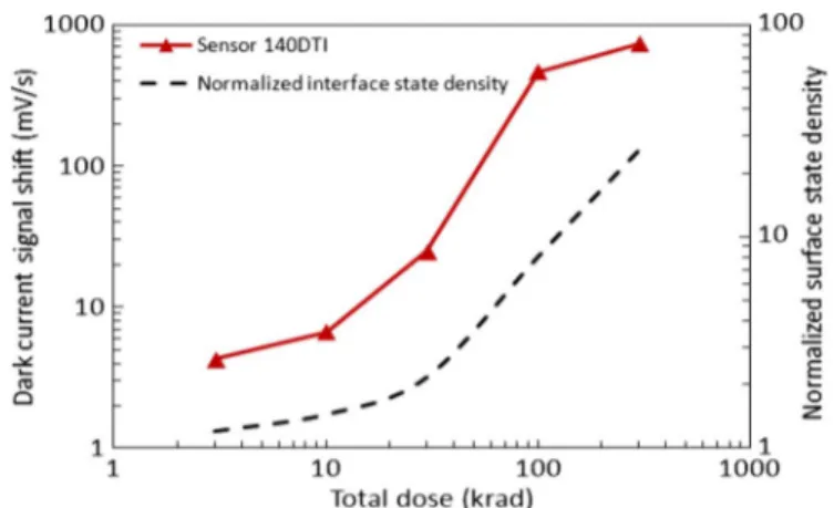
(2) With the generation velocity , the mean capture cross section, the thermal velocity, the intrinsic carrier density, the interface state density and the de-pleted interface area. From this equation, ratio of ex-tracted before and after irradiation provides us a piece of infor-mation about interface state density evolution on a fraction of TG gate oxide. The normalized values of with dark current signal shift degradation are represented on Fig. 13 for sensor 140DTI.
Evaluation of interface states degradation reveals the same trend with dark current evolution.
Then, a statistical approach of dark current is useful to com-ment the mean dark current under TG. Comparison of dark
cur-Fig. 13. Evolution of normalized Nit and dark current signal shift with TID for sensor 140DTI.
Fig. 14. Dark current signal histogram with TG OFF voltage for sensor 175STI at 30 .
rent distributions with before and after irradiation at 30 is on Fig. 14.
These diagrams show that dark current value at the peak of distribution is not particularly influenced with . However, distributions of white pixels increase with the two highest volt-ages for both plotted conditions ( and 30 ). The behavior of white pixels with TG bias explains the increase in mean dark current before and after irradiation. The evolution of distribution tail with TID shows that more and more pixels acquire huge dark current induced by TG interface state degra-dation.
C. Theoretical Analysis of Dark Current Under Irradiation
A study on the equations of dark current is proposed to pro-vide a coherent approach on phenomena at stake along trenches. Thus, electrons generated at the interface have to diffuse from interface to the photodiode according to diffusion equa-tion written below:
(3) With representing the minority carrier-lifetime and the diffusion length.
Fig. 15. Cross-section of pinned photodiode (a) and evolution of minority car-rier concentration along a cut line with irradiation induced stress (b).
Also, generation current of electrons, with conventions set in Fig. 15(a), is explained in [22] with the boundary condition at the interface linking the generation/recombination current and the diffusion current , as stated in (4):
(4) With the generation velocity of interface
states, the variation
of minority carrier density at the interface to be compared to concentration at thermal equilibrium, the acceptor concen-tration, q the electronic charge, the thermal velocity, cap-ture cross-sections of electrons and D the diffusion coefficient in the diffusion area.
The desertion of minority carriers at the edge of the depletion region in Fig. 15(b) imposes (5):
(5) Complete solution of dark current collected at the edge of depletion area gives:
(6) Considering (6), two realistic assumptions can be made to sim-plify this formula. The length L is supposed negligible com-pared to and it results in:
(7)
Fig. 16. Dark current reduction with different diffusion paths.
Then, it is supposed that generation processes at the interface are much more important than bulk generation ones on the length L
:
(8) This final expression shows that:
— thermal signature of dark current is characteristic of a dif-fusion behavior, according to term.
— dark current first increases linearly with degradation. — an important increase induces self-limitation of
mi-nority carriers diffusion characterized by a saturation of dark current collected, as sketched and reported in Fig. 15(b) and (9):
(9) Next, (7) and (8) suppose that dark current value can be modu-lated with the distance L. Fig. 16 illustrates the differences on multiple paths ( to ) from specific interface to the photodiode.
The greater the distance, the weaker dark current value is. Overall dark current contribution along trench is represented by a sum of elementary sections. Thus, this model success-fully explains at low doses why normalized contribution of deep trenches on Fig. 8. is weaker than shallow ones.
As the model is in good agreement with the saturation phe-nomenon at high TID, fits have been realized on each sensor in Fig. 17 on lin-lin scale.
The equation used for fitting is very similar to (8). Conclu-sions drawn in B) showed a strong correlation between dark current degradation and interface state density on gate oxide. Moreover, the main assumption based on a linear law between
TID and seems reasonable from 30
. Thus, the following expression is proposed: (10)
Fig. 17. Fits realized on normalized contributions of dark current. TABLE III
SUMMARY OFSATURATIONPOINTS ANDTRENCHVOLUME
These results well validate the saturation phenomenon de-scribed by theory in the second part of the graph.
As well, each trench presents different saturation doses, ex-cept for 175DTI where this phenomenon is not yet visible. A first assessment of saturation points with surrounding oxide’s volume is made on Table III.
Unfortunately, a clear trend cannot be extracted but physical argumentation will be proposed in the overall synthesis.
V. TEMPORALNOISEANALYSIS
Temporal noise performance conditions image quality espe-cially for low light level. This kind of measurement is basi-cally made during null integration time on two snaps. Differ-ences of these snaps suppress fixed pattern noise. Noise value is represented by standard deviation of pixels dispersion. Then, a special timing is used to discriminate the influence of respec-tively TG, SF and readout transistors by measuring noises of , and RD. Operations on squared stan-dard deviation enable identifying each contributor value.
All values of contributors are reported in Fig. 18 for sensor 175STI. The analysis of the temporal noise sources at room tem-perature reveals that most of the degradation comes from the SF transistor.
Another graph of relative temporal noise shift in Fig. 19 es-tablishes the main differences between sensors 175STI, 175DTI and 140DTI. It is established that 175STI degrades faster than others. Despite gate oxide thickness on sensor 175STI departs slightly from the others (65 vs 50 ), it reveals that oxide are too thin to explain charge effect accumulation.
Methodology of deducing normalized established in part IV B is useful here to assess gate oxide degradation on each
Fig. 18. Different contributors of temporal noise for sensor 175STI.
Fig. 19. Evolution of relative temporal noise shift with total ionizing dose on three different sensors.
TABLE IV
SUMMARY OFNORMALIZED EVOLUTIONUNDERTG
sensor. Table IV below resumes normalized for three sen-sors at 100 .
Values of interface state density on gate oxides reveal that dielectrics materials used for 175STI exhibit a twice more im-portant degradation at 100 . As TG and SF share the same gate oxide, properties at the interface are identical. Processes for gate oxide growth of sensor 175STI are first sus-pected. But the configuration of trench isolation needs also to be discussed. On sensor 175STI, any method has been used to dope isolation sidewalls. Interfaces and traps in the vicinity of STI are free to interact with SF channel as depicted in Fig. 20(a). On the contrary, DTI are systematically doped on sidewalls which quenches or at least minimize noise sources, as sketched on Fig. 20(b).
To enrich data set about temporal noise, SF distributions of sensors 175DTI and 175STI are respectively in Fig. 21 and Fig. 22. Peak variations in Fig. 21 are not significant
Fig. 20. Comparison of SF channel cross-sections in sensor 175STI (a) and in sensors 140DTI and 175DTI (b).
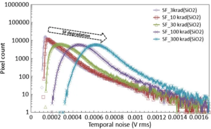
Fig. 21. Evolution of temporal noise distribution with TID for SF in sensor 175DTI.
Fig. 22. Evolution of temporal noise distribution with TID for SF in sensor 175STI.
until 30 with a slight transfer of population from peak to distribution tail. Major differences occur beyond 100 with a shift of temporal noise on values at the peak and on standard deviations. The same behavior is observed on sensor 175STI in Fig. 22 with significant variations above 30
.
At the moment, it seems difficult from results reported to point out the main contributor of the temporal noise degrada-tion. Two phenomena are here targeted between gate oxide and lateral trench degradation.
VI. DISCUSSION
Though every oxide (gate oxide, dielectric gapfill, buried oxide) have different process conditions (RTO, LPCVD, ), it has been evidenced that interface state degradation is strongly correlated with dark current saturation phenomena induced by trenches. Moreover, cross conclusions can be drawn between dark current and temporal noise results. Thus, the contribution of lateral trenches beyond 30 was considered to explain SF noise degradation. An evolution with oxide volume is proposed to explain the origin of saturation threshold and how it differs from a trench to another. Indeed, the physics and especially the diffusion mechanisms of radiolytic hydrogen released after irradiation, and discussed at the beginning of part IV, could be different, depending on aspect ratios of trenches and dielectrics volume inside. The properties of hydrogen dif-fusion in dielectrics, ruled by Fick’s law, would then condition the ability of interfaces to degrade during irradiation, inducing a different saturation threshold. This general assumption could be applied on all extended oxide parts and especially buried oxide. This additional oxide volume, releasing even more hydrogen, would explain the early saturation at 30
on 140DBOX sensor.
VII. CONCLUSION
Commercial advanced CMOS image sensors have been ir-radiated with a gamma-ray source. Despite these pixels with pinned photodiodes have not initially been developed to be radiation tolerant, it was observed on these devices a pretty good radiation hardness, with a sensor functionality preserved up to 300 . The exposition to the ionizing environ-ment has mainly impacted the dark current signal and temporal noise of the sensor. Indeed, it was shown that some technolog-ical characteristics like the pixel isolation or the buried oxide can modulate the degradation of dark current, respectively at high and low TID. Even if the nature of every oxide introduced is radically different and complex, an Arrhenius analysis of dark current highlights that TID induced damages were not due to a depleted interface, as previously observed on 3T CMOS image sensors. A mathematical model based on degradation along trench isolations is in good agreement with experimental data. In the future, it would be interesting to investigate the contribution of positive charges generated in oxides and compare them with the saturation effect induced by interface state density degrada-tion. As well, the evolution of temporal noise has been mainly attributed to TID induced damages in the SF of the pixel. It is correlated with interface state density of MOS gate oxide and/or isolation trenches.
Finally, the interface on top of the pinned photodiode did not appear to be the main degradation source after irradi-ation according to data measured on sensors embedding deep trench isolations. For further radiation hardness improvement, perimeter effects will have to be mitigated by new process con-ditions on trench isolations or by design variation.
ACKNOWLEDGMENT
The authors would like to thank process integration and imaging characterization teams for their support on techno-logical aspects and characterization techniques. Special thanks
are made to Guy Berger from the Université Catholique de Louvain for irradiation campaigns.
REFERENCES
[1] R. M. Guidash et al., “A 0.6 CMOS pinned photodiode color im-ager technology,” in Proc. Int. Electron Device Meeting, 1997, pp. 927–929.
[2] E. Fosssum, “CMOS image sensors: Electronic camera-on-a-chip,”
IEEE Trans. Electron Devices, vol. 44, no. 10, pp. 1689–1698, Oct.
1997.
[3] I. Inoue et al., “New LV-BPD (Low Voltage Buried Photo-Diode) for CMOS imager,” in Proc. Int. Electron Device Meeting, 1999, pp. 883–886.
[4] A. El Gamal and E. Eltoukhy, “CMOS image sensors,” IEEE Circuits
Des. Mag., vol. 21, no. 3, pp. 6–20, May–Jun. 2005.
[5] J. Leijtens et al., “Active pixel sensors: The sensor of choice for future space applications,” in Proc. SPIE, 2007, vol. 6744.
[6] G. R. Hopkinson et al., “Radiation effects in a CMOS active pixel sensor,” IEEE Trans. Nucl. Sci., vol. 47, no. 6, pp. 2480–2484, Dec. 2000.
[7] B. Pain et al., “Hardening CMOS imagers: Radhard-by-design or rad-hard-by-foundry,” in Proc. SPIE, 2004, vol. 5167, pp. 101–110. [8] V. Goiffon et al., “Analysis of total dose-induced dark current in
CMOS image sensors from interface state and trapped charge density measurements,” IEEE Trans. Nucl. Sci., vol. 57, no. 6, pp. 3087–3094, Dec. 2010.
[9] J. Bogaerts et al., “Total dose and displacement damage effects in a radiation-hardened CMOS APS,” IEEE Trans. Electron. Devices, vol. 50, no. 1, pp. 84–90, Jan. 2003.
[10] P. Rao et al., “Degradation of CMOS image sensors in deep-submicron technology due to -irradiation,” Solid-State Electron., vol. 52, no. 9, pp. 1407–1413, Sep. 2008.
[11] J. Tan and A. Theuwissen, “Total ionizing dose effects on 4-transistor CMOS image sensor pixels,” in Proc. IEEE Int. Conf. Electron Devices
and Solid-State Circuits, Dec. 2010, pp. 1–4.
[12] J. Tan et al., “4T CMOS image sensor pixel degradation due to x-ray ra-diation,” in Proc. Int. Image Sensor Workshop, Hokkaido, Japan, 2011. [13] A. Theuwissen, “CMOS image sensors: State-of-the-art and future per-spectives,” in Proc. Eur. Solid-State Device Research Conf., 2007, pp. 21–27.
[14] A. Tournier et al., “Pixel-to-pixel isolation by deep trench technology: Application to CMOS image sensor,” in Proc. Int. Image Sensor
Work-shop, Hokkaido, Japan, 2011.
[15] T. R. Oldham and F. B. McLean, “Total ionizing dose effects in MOS oxides and devices,” IEEE Trans. Nucl. Sci., vol. 50, no. 3, pp. 483–499, Jun. 2003.
[16] J. Prima et al., “Improved color separation for a backside illuminated image sensor with 1.4 pixel pitch,” in Proc. Int. Image Sensor
Workshop, Bergen, Norway, 2009.
[17] H. L. Hugues and J. M. Benedetto, “Radiations effects and hardening of MOS technology: Devices and circuits,” IEEE Trans. Nucl. Sci., vol. 50, no. 3, pp. 500–521, Jun. 2003.
[18] H. I. Kwon et al., “The analysis of dark signals in the CMOS APS im-agers from the characterization of test structures,” IEEE Trans.
Elec-tron Devices, vol. 51, no. 2, pp. 178–184, Feb. 2004.
[19] A. S. Grove and D. J. Fitzgerald, “Surface effects on p-n junctions: Characteristics of surface space-charge regions under non-equilibrium conditions,” Solid-State Electron., vol. 9, pp. 783–806, 1966. [20] D. M. Fleetwood et al., “Effects of hydrogen transport and reactions on
microelectronics radiation response and reliability,” J. Microelectron.
Reliab., vol. 42, pp. 523–541, 2002.
[21] H. Han et al., “Evaluation of a small negative transfer gate bias on the performance of 4T CMOS image sensor pixels,” in Proc. Int. Image
Sensor Workshop, Ogunquit, ME, 2007, Session 12.
[22] S. M. Sze, Physics of Semiconductor Devices, 2nd ed. Hoboken, NJ: Wiley, 1981, p. 56.