To cite this document
: GOIFFON Vincent, VIRMONTOIS Cédric, MAGNAN Pierre,
CERVANTES Paola, GAILLARDIN Marc, GIRARD Sylvain, PAILLET Philippe,
MARTIN-GONTHIER Philippe. Identification of radiation induced dark current sources in pinned photodiode
CMOS image sensors. In: Radiation Effects on Components and Systems Conference, 19-23 Sept.
2011, Sevilla, Spain.
This is an author-deposited version published in:
http://oatao.univ-toulouse.fr/
Eprints ID: 5077
Any correspondence concerning this service should be sent to the repository administrator:
[email protected]
Identification of Radiation Induced
Dark Current Sources in
Pinned Photodiode CMOS Image Sensors
V. Goiffon, Member, IEEE, C. Virmontois, Student Member, IEEE, P. Magnan, Member, IEEE, P. Cervantes,
M. Gaillardin, Member, IEEE, S. Girard, Member, IEEE, P. Paillet, Senior Member, IEEE,
P. Martin-Gonthier, Member, IEEE
Abstract—This paper presents an investigation of Total Ioniz-ing Dose induced dark current sources in Pinned PhotoDiodes (PPD) CMOS Image Sensors based on pixel design variations. The influence of several layout parameters is studied. Only one parameter is changed at a time enabling the direct evaluation of its contribution to the observed device degradation. By this approach, the origin of radiation induced dark current in PPD is localized on the pixel layout. The PPD peripheral STI does not seem to play a role in the degradation. The PPD area and an additional contribution independent on the pixel dimensions appear to be the main sources of the TID induced dark current increase.
I. INTRODUCTION
P
INNED PHOTODIODES (PPD) are widely used in state-of-the-art CMOS Image Sensors (CIS) for high and low end commercial applications such as cellphone where the market trend goes to decrease the pixel size as much as possible. These photodetectors are optimized for pixel pitches as small as 1 µm and are not directly usable for scientific applications which usually require larger photodetector sizes (most often between 5 and 15µm). This is one of the reasons why many scientific applications still use the classical CMOS PN junction based pixel (also called 3T-pixel in its simplest form), but the benefit of pinned photodiode leads to a growing number of high performance scientific CIS based on these devices [1]. However, the behavior of PPD based sensors in ionizing environment is not well understood today and this can limit their use in applications such as nuclear and particle physics, space applications or medical imaging.Only few papers [2]–[6] have been published on the ra-diation tolerance of the pinned photodiode and its associated Transfer Gate (TG). All these studies pointed out that ionizing radiation induces a dark current increase in PPD sensors as in classical PN junction based pixels. From these studies, it cannot be clearly inferred what are the main sources of this dark current increase in such pixels. Shallow Trench Isolation (STI) and the TG are often suggested to be the main sources of radiation induced dark current [2], [4], [6], but there is no unquestionable evidence of these conclusions in
V. Goiffon, C. Virmontois, P. Magnan,P. Cervantes and P. Martin-Gonthier are with Universit´e de Toulouse, ISAE, Toulouse, 31055, France (Phone: +33 5 6133 8093, Fax: +33 4 6133 8345, e-mail: [email protected]).
M. Gaillardin, S. Girard and P. Paillet are with CEA, DAM, DIF F91297 Arpajon, France. N P Transfer Gate (TG) STI PMD STI N Floating Diffusion (FD) Pinned PhotoDiode (PPD) Gate oxide Silicide block oxide VDD RST ROW VDD Readout node T1 T2 T3 Pixel output
Space Charge Region (SCR) dSTI
Fig. 1. Pinned photodiode pixel cross-section with 4T pixel architecture.
SHS SHR RST
TG Integration time
Inter sample time
Fig. 2. 4T PPD pixel timing diagram illustration showing the integration time and the inter-sample time.
well designed (i.e. with STI far enough from the PPD [2], [7]) and well biased pinned photodiode (i.e. with the TG completely accumulated during integration [8]). Moreover, since the radiation induced dark current sources are still not precisely localized on the pixel layout, efficient radiation-hardening-by-design guidelines cannot be established for PPD pixels.
In this paper, we present an investigation of Total Ionizing Dose (TID) induced dark current sources in PPD-CIS based on pixel design variations. The influence of several layout parameters is studied. Only one parameter is changed at a time enabling the correlation between the observed degradation and each parameter independently. The purpose of this work is to localize the radiation induced dark current sources in PPD CIS. Such identification is necessary to improve the radiation hardness of PPD and also to improve the reliability of CIS radiation tests.
SUMMARY OF THE STUDIED PIXEL LAYOUTS. PERIM.STANDS FOR
PERIMETER, WTGFORTGWIDTH ANDCVFFOR CONVERSION FACTOR.
Name PPD PPD WTG FD CVF Area Perim. Perim. µV/e−
Com 20µm2 39 µm 1.6 µm 3.5 µm 75 Area1 40µm2 39µm 1.6 µm 3.5 µm 75 Area2 60µm2 39µm 1.6 µm 3.5 µm 75 Area3 82µm2 39µm 1.6 µm 3.5 µm 75 Perim1 20µm2 33µm 1.6 µm 3.5 µm 75 Perim2 20µm2 25µm 1.6 µm 3.5 µm 75 Perim3/Ref 20µm2 18µm 1.6 µm 3.5 µm 75 TG1 20µm2 39µm 1.6 µm 29µm 16 TG2 20µm2 39 µm 5.8 µm 29µm 16 TG3 20µm2 39µm 10.0 µm 29µm 16 TG4 20µm2 39µm 14.0 µm 29µm 16 FD1 20µm2 39 µm 1.6 µm 29µm 16 FD2 20µm2 39µm 1.6 µm 29µm 23 FD3 20µm2 39µm 1.6 µm 29µm 35 PPD TG FD WTG HPPD LPPD LFD STI
Fig. 3. Pinned photodiode pixel layout illustration with the parameters of interest in this work (PPD dimensions, TG width and FD perimeter).
II. SPECIFICITIES OF PINNED PHOTODIODES
A cross-section of a typical pinned photodiode is presented in Fig. 1. As can be seen in the figure, the simplest pixel architecture based on pinned photodiode uses one more tran-sistor than the well-known three-trantran-sistor-per-pixel design (3T-APS). This architecture is very often called 4T-PPD CIS or 4T-PPD Active Pixel Sensors (APS). It is important to notice that the pinned photodiode in more-than-four-transistor-PPD-pixels will behave the same as in a 4T-PPD pixel, therefore un-derstanding the 4T-PPD behavior in ionizing environment will help understanding the behavior of any pixel architecture based on PPD. In this figure, one can identify the three transistors used in 3T-pixel for resetting the floating diffusion, selecting the pixel and amplifying the collected charge converted into a voltage [9]. This conversion occurs in the Floating Diffusion (FD), which corresponds to the photodiode in a 3T-pixel except that it is a shallow N+/Pwell junction instead of an Nwell/Pepi photodiode. The two major differences with the 3T architec-ture are the pinned photodiode itself and the transfer gate. The pinned photodiode can be described as a volume of N-doped region surrounded by a P doping. In this configuration, an optimized pinned photodiode is fully depleted and under non-equilibrium conditions, at the beginning of integration, acting as a potential well for photo-generated electrons. The surface P-doping concentration is high enough to prevent the space charge region of the photodiode to reach the top oxide
DESCRIPTION OF THE STUDIED ALTERNATIVEPPDLAYOUTS.
Name Description Round Round PPD (no corner) RadTol Radiation tolerant design based on [3] STI 0.5 PPD withdSTI= 0.5 µm
STI 0.75 PPD withdSTI= 0.75 µm
STI 1.0 PPD withdSTI= 1µm
PPD
TG FD
Gate/STI
Fig. 4. Pinned photodiode layout illustration of the radiation tolerant structure based on the concept proposed in [3].
and the Pwells prevent the depleted region from reaching the STI sidewalls. It should be emphasized that, contrary to 3T pixels, the space charge region of an optimized PPD does not touch any oxide, which should lead to extremely good ionizing radiation hardness. At the end of integration (see Fig. 2 for a detailed timing diagram), the photo-generated electrons collected by the PPD potential well are transferred to the FD for being readout. The FD is reset before the transfer and its value is sampled thanks to the SHR digital signal. Another sample is taken after the transfer (thanks to SHS), and the difference between these two samples allows to recover the amount of collected charges.
III. EXPERIMENTAL DETAILS
The studied sensors, divided in 32x32-pixel-regions, have been manufactured using a0.18µm CMOS process dedicated to CIS. The selected pixel size is 10 × 20 µm2
to allow the design of all the layout variations used in this study. The details of the manufactured pixels with geometric variation are presented in Tab. I. The geometric layout variations used for the study are presented in Fig. 3. Among these structures, pixel Perim3 will be used as a reference pixel since its photodiode dimensions are close to what can be found in a realistic6 µm-pitch 4T-PPD pixel. In addition to these pixels, five alternative layouts have also been tested. They are described in Tab. II. The Round pixel has no corner and the photodiode layout of the RadTol pixel is based on the radiation tolerant design proposed in [3], as illustrated in Fig. 41. The layout of pixels
STI 0.5, 0.75 and 1.0 are the same as the reference pixel (Perim3) but with STI recessed 0.5, 0.75 and 1.0 µm away from the photodiode layer (instead of0.3 µm for all the other structures). These recess distances correspond to the distance dSTI shown at the top left of Fig. 1.
Dark current measurements were performed at 22◦C
reg-ulated temperature, with no illumination. The dark current 1Since the layout was not described in the original paper (only the
cross-section was), the pixel layout used in this study may differ in some points from the layout used in [3].
−0.80 −0.6 −0.4 −0.2 0 0.2 0.4 0.6 10 20 30 40 50 60 70 80 VLOTG (V) I dark (e−/s)
Fig. 5. Reference pixel (pixel Perim3) dark current evolution with transfer gate off voltage (VLOTG) before irradiation.
0 20 40 60 80 100 −50 0 50 100 150 200 250 Area (µm2) Idark (e−/s) V LOTG=0V V LOTG=−0.1V V LOTG=−0.2V V LOTG=−0.3V V LOTG=−0.4V V LOTG=−0.5V Highest slope: 2.0 e−/s/µm2 Lowest slope: 1.8 e−/s/µm2
Fig. 6. Dark current variation with photodiode area for several VLOTG,
before irradiation (pixels Com, Area1, Area2 and Area3).
extraction was realized by averaging one hundred dark frames for several increasing integration time (between ten and fifty points in the linear region), and by computing a linear regres-sion of the dark frame voltage as a function of integration time. Some non-linearities were observed at the highest TID levels. In this case, the worst case dark current was used for the study (i.e. the linear regression was performed in the maximum slope region).
The test devices were exposed unbiased to 10 keV X-rays, at CEA-DIF, thanks to an ARACOR model 4100 semi-conductor X-ray irradiator. The absorbed TID ranges from 10 krad(SiO2) to 150 krad(SiO2) and the dose rate was about
100 rad(SiO2)/s.
IV. RESULTS AND DISCUSSION
A. Extraction of geometric contributions
During integration, the transfer gate is biased to VLOTG,
which is supposed to turn it off. The value of VLOTG has
a strong influence on dark current as shown in Fig. 5 and as discussed in [8], [10], [11]. At zero voltage, the depletion region of the transfer gate merges with the depletion region of the PPD, leading to an intense dark current due to interface states located below the transfer gate. At negative voltage (in
15 20 25 30 35 40 0 10 20 30 40 50 60 70 80 90 Perimeter (µm) I dark (e−/s) V LOTG=0V V LOTG=−0.1V V LOTG=−0.2V V LOTG=−0.3V V LOTG=−0.4V V LOTG=−0.5V
Average slope ≈ 0.2 e−/s/µm)
Fig. 7. Dark current variation with photodiode perimeter for several VLOTG,
before irradiation (pixels Com, Perim1, Perim2 and Perim3).
0 5 10 15 20 25 30 0 10 20 30 40 50 60 70 80 FD length (µm) I dark (e−/s) V LOTG=0V V LOTG=−0.1V V LOTG=−0.2V V LOTG=−0.3V V LOTG=−0.4V V LOTG=−0.5V
Slope between −0.12 and +0.21 e−/s/µm
Fig. 8. Dark current variation with floating diffusion perimeter for several VLOTG, before irradiation (pixels Com, FD1, FD2 and FD3).
the−0.5; −0.7 V range), the transfer gate is in accumulation regime leading to the disappearance of the TG depleted region and preventing the PPD space charge region to reach the oxide interface. Despite the intrinsic differences between a pinned photodiode and a conventional CMOS diode, this effect corresponds well to what is observed in a gated diode [12]. When the TG voltage is too low (i.e. below −0.7 V), it leads to an Electric Field Enhancement (EFE) of the leakage current [13]. It has been concluded in [14], that this EFE is a Trap Assisted Tunneling (TAT) effect as usually observed in MOSFETs [15] when a voltage much lower than the threshold voltage is applied on the gate (once again, as in a classical gated diode). The optimal accumulation voltage selected for this study is−0.6 V since it leads to the minimum dark current with a limited TAT EFE effect.
The PPD dark current can be decomposed in several con-tributions:
Idark= Ja×APPD+Jp×PPPD+JTG×WTG+JFD×PFD+I0
(1) with APPD the PPD area, PPPD its perimeter, WTG the
transfer gate width,PFDthe floating diffusion perimeter andI0
the remaining contribution which is not a function of the other parameters. In order to discriminate the different contributions,
0 2 4 6 8 10 12 14 16 0 100 200 300 400 500 TG width (µm) Idark (e−/s) V LOTG=0V V LOTG=−0.1V V LOTG=−0.2V V LOTG=−0.3V V LOTG=−0.4V V LOTG=−0.5V
Fig. 9. Dark current variation with transfer gate width for several VLOTG,
before irradiation (pixels TG1, TG2, TG3 and TG4).
the evolution of dark current with each of these parameters is presented, before irradiation, in the following figures.
Fig. 6 shows the evolution of dark current with the PPD area and for several VLOTG. A clear correlation between the
PPD area and the dark current appears and is quantified by the slope, Ja, of the linear regression (dashed line) between
the area and the dark current. It is important to notice that the TG off voltage does not have any significant influence on the area contribution Ja which remains approximately equal
to 1.9 e−.s−1.µm−2. This area contribution is most likely
dominated by the diffusion current coming from the silicon neutral volume surrounding the PPD depletion region.
Contrary to the area current source, Fig. 7 shows that there is no significant contribution from the PPD perimeter (|Jp| <
1 e−.s−1.µm−1). Hence, the peripheral STI does not seem
to play an important role in the pre-irradiation dark current in these devices. Exactly the same conclusion can be made on the influence of the FD perimeter (|JF D| < 0.3 e−.s−1.µm−1),
as shown in Fig. 8. This last result could have been expected from the timing diagram (Fig. 2). Indeed the dark current is by definition the evolution of the output voltage with integration time. Since the FD is reset just before the transfer, only the charge generated in the FD during the inter sample time can contribute to the measured voltage. As this inter-sample time does not change with integration time, the FD contribution cannot be seen. The conclusion would be different in a snapshot PPD pixel in which the sampled signal is stored on a floating diffusion for a significant amount of time before being read. In this case, the dimension of the floating diffusion used to store the signal would have a large impact on the resulting dark signal.
As regards the TG contributionJTG, it can clearly be seen
in Fig. 9 that it is very dependent onVLOTG, as expected [8],
[10], [11]. At VLOTG = 0, this contribution is very large
(JTG≈ 30 e−.s−1.µm−1) whereas is tends to zero when the
TG approach the accumulation regime.
We have seen that when the TG is accumulated, the only contribution dependent on the photodiode dimension is Ja.
Thus the I0 contribution is simply determined by extracting
0 50 100 150 101 102 103 10 TID (krad(SiO 2)) I dark (e−/s) IC1 V LOTG=0V IC2 V LOTG=0V IC3 V LOTG=0V IC1 V LOTG=−0.6V IC2 V LOTG=−0.6V IC3 V LOTG=−0.6V
Fig. 10. Reference pixel dark current evolution with TID (pixel Perim3). The figure also shows how many devices have been used and which TID has been received by each device. In the following figures, only one value is given by TID level (the average value).
0 50 100 150 −4 −3 −2 −1 0 1 2 3 4 TID (krad(SiO2)) Jp (e−/s/ µ m)
Fig. 11. Perimeter dark current linear densityJp as a function of total
ionizing dose.
the y-axis intercept (for an area= 0 µm2
) in Fig. 6. It can be seen thatI0 is negligible before irradiation.
B. Evolution with irradiation
Fig. 10 presents the evolution of dark current with TID of the reference pixel (Perim3) with two VLOTG biasing
conditions: depleted (VLOTG = 0 V) and accumulated
(VLOTG= −0.6 V) during integration. The average dark
cur-rent increases with TID in both cases (and a slight saturation effect can be observed at the highest TID level when the TG is depleted). However, about one order of magnitude of reduction is achieved when the TG is accumulated during integration. Further insight into this degradation is given by looking at each contribution separately. It should also be noticed that this figure shows how many IC have been used per TID level during this study. In the following, when more than one device were irradiated at a given TID level, the average dark current value is provided.
The perimeter contribution (in which the peripheral STI contribution is included) stays in the uncertainty of the slope extraction process even at 150 krad(SiO2) (Fig. 11). Hence,
0 50 100 150 200 250 300 I dark (e−/s) Ref.
Round RadTol. STI 0.5 STI 0.75 STI 1.0
Fig. 12. Dark current of the alternative photodiode layouts after 75 krad(SiO2) withVLOTG = −0.6 V. The differences between structures
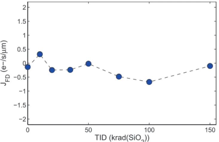
are small enough to be attributed to device mismatches and measurement errors. 0 50 100 150 −2 −1.5 −1 −0.5 0 0.5 1 1.5 2 TID (krad(SiO2)) J FD (e−/s/ µ m)
Fig. 13. Floating diffusion dark current linear densityJFDas a function of
total ionizing dose.
in opposition to what is generally inferred, the peripheral STI does not seem to have any influence on the radiation induced dark current2(in this TID range). This conclusion is confirmed
by the dark current measured on the structures with larger STI recess distancedSTI, as illustrated in Fig. 12. Indeed, it can be
seen in the figure that there is no significant difference between the dark current measured after irradiation on the reference pixel (with dSTI = 0.3 µm) and the dark currents measured
on the pixels with a larger recess distance (dSTI= 0.5 , 0.75
and 1.0 µm). Similar conclusions can be drawn on the FD 2It agrees well with the results presented in [6] but seems to contradict the
conclusion drawn on PPD with very small pixel pitches [16] (around 1µm). Indeed, in this last study, the authors suggest that one of the radiation induced dark current source comes from the perimeter of the PPD. This discrepancy with the work presented here is attributed to two main factors: 1) The dark current is so low (well below 1 e−/s at room temperature) in these small
pitch state-of-the-art devices than it can reveal other dark current sources that are not visible here. 2) in small pitch (below 2µm) PPD, the pixels are drawn by using the minimum sizes that bring good performance before irradiation. It means that, for example, the recess distancedSTIbetween the PPD and the
STI is likely to be smaller than the 0.3 µm used in our work. This distance might be tuned to the optimum value that lead to the minimum dark current before irradiation. However, this minimum distance might be too small to mitigate the influence of the peripheral STI on the overall PPD dark current.
0 50 100 150 0 2 4 6 8 10 TID (krad(SiO2)) J a (e−/s/ µ m 2 )
Fig. 14. Dark current area densityJaas a function of total ionizing dose.
0 50 100 150 0 100 200 300 400 500 TID (krad(SiO2)) J TG (e−/s/ µ m) V LOTG=0V V LOTG=−0.6V
Fig. 15. Transfer gate dark current linear densityJTGas a function of total
ionizing dose.
contribution to the overall dark current as can be seen in Fig. 13.
As regards the area contribution, Fig. 14 shows that Ja does not change significantly up to 75 krad(SiO2). At
100 krad(SiO2), a slight increase is observed. It is confirmed
by a much larger rise at 150 krad(SiO2). The only source
of TID induced dark current that can be a function of the PPD area is the top oxide interface (silicide block oxide interface in Fig. 1). There are two possible mechanisms that can explain this observation: 1) The radiation induced trapped charge density becomes large enough to change the electrostatic potential distribution above the pinned photodiode (by reducing the effective doping concentration of the P+ pinning layer), leading to the extension of the PPD depletion to the top oxide interface (as explained in [17]). 2) The large amount of interface states generated in the top oxide/silicon interface by the ionizing radiation induce a large diffusion current contribution that becomes larger than the diffusion current contribution coming from the silicon neutral volume.
If the TG is biased in accumulation, it can be seen in Fig. 15 that the ionizing radiation does not increase the JTG
contribution whereas a huge rise can be seen in the case where VLOTG = 0 V. This large increase is most likely due to the
0 50 100 150 0 1000 2000 3000 4000 I 0 (e − /s) @ V LOTG = 0 V TID (krad(SiO2)) 0 50 100 1500 100 200 300 400 I 0 (e − /s) @ V LOTG = −0.6 V V LOTG = 0 V V LOTG = −0.6 V
Fig. 16. Dark current offsetI0as a function of total ionizing dose. interface states generated in the depleted region of the transfer gate (gate oxide and possibly STI sidewalls).
The most surprising result is presented in Fig. 16. This figure shows that the contributionI0, independent of the design
variations, increases much with TID in both VLOTG bias
conditions. However, this radiation induced parasitic current can be reduced by about a factor of ten when the TG is biased in accumulation during integration. This last result demonstrates that this contribution is directly influenced by the TG voltage. The possible origin of I0 is discussed in
sec. V-A. It is also interesting to notice the decrease of dark current at 150 krad(SiO2). This effect seems correlated with
the increase in area contribution Ja and could also possibly
be linked to the change of electrostatic potential distribution (due to a degradation of the P+ pinning layer).
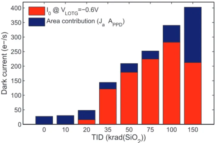
Now that each dark current source has been de-correlated, it is interesting to look at their contribution relatively to each other. This is what is presented in Fig. 17 and Fig. 18. In these bar charts, each color represents a dark current source and the total bar height is equal to the total dark current measured. The dark current source contributions have been evaluated by using (1), the previously determined values and the area and perimeter of the reference pixel (Perim3) given in Tab. I.
When the TG is biased to 0 V during integration, it can clearly be seen that before irradiation, the two main contrib-utors are the transfer gate linear current density JTG and the
dark current area density Ja. After the first irradiation step,
I0becomes the main source of dark current. The dark current
attributed to the TG width also rises significantly and brings between 15 and 40% of the total radiation induced dark cur-rent. The area dark current remains negligible in this biasing condition, despite a noticeable increase at 150 krad(SiO2).
When the TG is biased into accumulation during integration, the dark current from the TG width disappears and the current from the area dominates up to 20 krad(SiO2). As
already mentioned, this last contribution stays constant up to 100 krad(SiO2). The I0 source begins to appear in this
regime at 20 krad(SiO2) and dominates the total current from
35 krad(SiO2) to 150 krad(SiO2). It should be emphasized
that at this last TID level, the area contribution represents about 40% of the total current whereas it was below 15%
0 10 20 35 50 75 100 150 0 1000 2000 3000 4000 5000 TID (krad(SiO2))
Dark current (e−/s)
0 LOTG TG width contribution (J TG LTG) Area contribution (J aAPPD) 0 0 20 40 60 80
Fig. 17. Reference pixel (Perim3) dark current forVLOTG= 0 Vshowing
the contribution of each dark current source to the total current.
0 10 20 35 50 75 100 150 0 50 100 150 200 250 300 350 400 TID (krad(SiO2))
Dark current (e−/s)
I
0 @ VLOTG=−0.6V
Area contribution (J
aAPPD)
Fig. 18. Reference pixel (Perim3) dark current for VLOTG = −0.6 V
showing the contribution of each dark current source to the total current.
at the previous step. It suggests a strengthening of the area contribution over theI0 source at higher TID levels.
V. DISCUSSION
A. Possible origins ofI0 and consequences on RHDB
The main contribution,I0, to the TID induced dark current
rise is a current source which is not dependent on the design variations studied in this work. By looking at Fig. 3, one can see that the two parts of the photodiode layout that are common to all the pixels listed in Tab .I are: 1) the corner of the PPD and 2) the lateral edges (perpendicular to the PPD area) of the TG. The PPD corners cannot be the source ofI0
becauseI0is strongly dependent onVLOTGwhereas the corner
of the PPD area is too far from the TG to be influenced by its voltage. This is confirmed by the measurements performed on the Round diode, which are presented in Fig. 12. Indeed, removing the corners by drawing a completely round PPD does not change the total current, which is dominated by I0
at this TID (see Fig. 18).
As regards the TG lateral edges, one can see in Fig. 3 that it can be divided in two regions. The first is the part of the TG that is located over the active area (i.e. with no STI). The second is the part of the TG that is placed over the STI, to
0 50 100 150 101 102 103 104 105 TID (krad(SiO 2)) I dark (e−/s) 4T PPD V LOTG=0V 4T PPD V LOTG=−0.6V 3T RHDB 3T
Fig. 19. Dark current evolution with TID: comparison between a conven-tional 3T pixel, a Radiation-Hardened-By-Design (RHDB) 3T pixel (surround P+ [18]) and the reference 4T PPD pixel (Perim3). The equivalent pixel pitch is about 6µm. The 3T pixel results, measured on 2×5 µm2photodiodes [18],
are normalized to the reference pixel pinned photodiode size (4.5 × 4.5 µm2)
assuming a direct proportionality of 3T pixel dark current on photodiode perimeter(as demonstrated in [19]).
allow the formation of the contact via. Once again, Fig. 12 allows us to go a little further. The measurements performed on the RadTol structures show no significant improvement on the TID induced dark current generation3. By comparing Fig. 3
and Fig. 4, it can be noticed that the TG edge located over the PPD region changes much between the two layouts: this part of the TG is longer in the case of the RadTol design and there are also more TG corners than in the standard design of Fig. 4. On the other hand, the part of the TG that overlaps the STI is pretty similar in both cases. These results suggest that the source of I0 could be due to the design of the TG in the
transition region where the TG approaches the STI.
Based on these results, it is inferred that the main source of dark current comes from the TG region, near the STI. If this hypothesis is validated, changing the design of the TG in this specific region should have a strong impact on the I0 source and mitigation techniques could probably be
found. As regards the radiation induced area contribution that arises above 100 krad(SiO2), there is apparently no way of
mitigating it by design (except by reducing the area). If the increase of the area contribution is confirmed at higher TID levels (especially on other devices and technologies), it could be a serious limitation for the use of 4T PPD in high TID applications.
B. Comparison between 4T-PPD and 3T CIS
Radiation hardness of CIS is pretty difficult to compare from one work to another. Among the numerous reasons for that, one can cite: the different dimensions, the different processes and technology nodes used (and the associated differences in pre-irradiation dark current values), the different designs, the differences in measurements conditions and measurement units with most often no way of extrapolating correctly the 3This could be due to a slight difference between the layout used in [3]
and the one used here.
results (due to the absence of photodiode layout dimension). Moreover, since, to our knowledge, the influences of all the dimensions of the PPD on the radiation induced dark current were never de-correlated before, it was difficult to extrapolate the results achieved on one PPD layout to the values measured on another imager. What is very often done is to express the dark current in an area current density unit (e.g.nA/cm2
), usually referred to the pixel pitch (instead of the PPD area), and then it is extrapolated to another pixel pitch by assuming direct proportionality to the pixel pitch. This work demonstrates that such technique would lead to wrong interpretations on 4T-PPD CIS.
Fortunately, the devices studied in this work have been manufactured with the same process as the work performed on 3T-CIS presented in [18]. Moreover, it is well-known [20], and it is regularly confirmed (e.g. as shown in [19]), that radi-ation induced dark current in 3T-CIS mainly comes from the photodiode perimeter. Therefore, the results presented in [18] can directly be compared to the measurement performed on the studied 4T-PPD pixels only by multiplying the 3T-CIS results by the perimeter ratio of the 4T-PPD and 3T CIS. Such comparison is shown in Fig. 19. It can clearly be seen that, as expected from the lower pre-irradiation dark current values of 4T-PPD CIS compared to 3T CIS, the TID induced dark current increase of pinned photodiodes is more than one order of magnitude below the standard 3T design. It can even be more than two orders of magnitude lower when the TG is accumulated during integration. It is pretty interesting to notice that both 3T and 4T-PPD dark current trends with TID appear pretty similar (despite the difference of order of magnitude). Moreover, the relative increase (i.e. the dark current increase divided by the dark current level before irradiation) is almost the same between the two sensor technologies. It should also be emphasized that the gap between the two technologies is significantly reduced when a 3T radiation hardened design is used and more work is needed to determine if 4T-PPD CIS will still exhibit the best behavior at a higher TID level. Further-more, dark current increase is the main reported degradation but more studies are necessary to determine whether the other 4T-PPD CIS characteristics are degraded by ionizing radiation.
VI. SUMMARY
The localization of dark current sources before and after exposure to ionizing radiation has been investigated in Pinned Photodiode CMOS Image Sensors. The contributions of the area, the perimeter, the transfer gate width and the floating diffusion length to the TID induced dark current have been de-correlated for the first time in PPD-CIS. It has been shown that up to 150 krad(SiO2), the PPD perimeter and the FD
perimeter do not contribute to the overall dark current. The TG width does not contribute to the radiation induced dark current either if biased in accumulation. The remaining radiation induced dark current sources are: a contribution from the area of the PPD, most likely coming from the top oxide radiation induced defects and a contribution independent on pixel design variations. The results presented here suggest that the latter dark current source is related to the region of
the TG that is located near the STI, for allowing the contact via formation. Changing the design of the TG in this area is thus expected to change the radiation hardness of the devices. This identification of degradation sources in PPD CIS will help improving our understanding of irradiated PPD behaviors and will help finding efficient radiation-hardening-by-design solutions.
ACKNOWLEDGMENT
The authors are grateful to Franck Corbi`ere and S´ebastien Rolando, from ISAE, for their invaluable support on circuit design. We would also like to thank Manuel Innocent and Yannick De Wit, from ON-Semiconductor, for their helpful comments.
REFERENCES
[1] B. Fowler, C. Liu, S. Mims, J. Balicki, W. Li, H. Do, J. Appelbaum, and P. Vu, “A 5.5 Mpixel 100 frames/sec wide dynamic range low noise CMOS image sensor for scientific applications,” in Procs of SPIE, vol. 7536, 2010, p. 753607.
[2] P. R. Rao, X. Wang, and A. J. P. Theuwissen, “Degradation of CMOS image sensors in deep-submicron technology due to γ-irradiation,” Solid-State Electron., vol. 52, no. 9, pp. 1407–1413, Sep. 2008. [3] M. Innocent, “A radiation tolerant 4t pixel for space applications,” in
Proc. IISW, 2009.
[4] R. E. Coath, J. P. Crooks, A. Godbeer, M. D. Wilson, Z. Zhang, M. Stanitzki, M. Tyndel, and R. A. D. Turchetta, “A low noise pixel architecture for scientific CMOS monolithic active pixel sensors,” IEEE Trans. Nucl. Sci., 2010.
[5] P. Vu, B. Fowler, B. Rodricks, J. Balicki, S. Mims, and W. Li, “Evaluation of 10MeV proton irradiation on 5.5 Mpixel scientific CMOS image sensor,” in Proc. SPIE, vol. 7826, no. 60, 2010.
[6] J. Tan, B. Bttgen, and A. Theuwissen, “4t cmos image sensor pixel degradation due to x-ray radiation,” in Proc. IISW, 2011.
[7] H. Kwon, I. Kang, B. Park, J. Lee, and S. Park, “The analysis of dark signals in the CMOS APS imagers from the characterization of test structures,” IEEE Trans. Electron Devices, vol. 51, no. 2, pp. 178–184, Feb. 2004.
[8] T. Watanabe, J.-H. Park, S. Aoyama, K. Isobe, and S. Kawahito, “Effects of negative-bias operation and optical stress on dark current in CMOS image sensors,” IEEE Trans. Electron Devices, vol. 57, no. 7, pp. 1512 –1518, Jul. 2010.
[9] E. R. Fossum, “CMOS image sensors: electronic camera-on-a-chip,” IEEE Trans. Electron Devices, vol. 44, no. 10, pp. 1689–1698, Oct. 1997.
[10] H. Han, H. Park, P. Altice, W. Choi, Y. Lim, S. Lee, S. Kang, J. Kim, K. Yoon, and J. Hynecek, “Evaluation of a small negative transfer gate bias on the performance of 4t CMOS image sensor pixels,” in Proc. IISW, 2007.
[11] B. Mheen, Y. Song, and A. Theuwissen, “Negative offset operation of four-transistor CMOS image pixels for increased well capacity and suppressed dark current,” IEEE Electron Device Lett., vol. 29, no. 4, pp. 347–349, 2008.
[12] A. S. Grove and D. J. Fitzgerald, “Surface effects on p-n junctions: Characteristics of surface space-charge regions under non-equilibrium conditions,” Solid-State Electron., vol. 9, no. 8, pp. 783–806, Aug. 1966. [13] G. Vincent, A. Chantre, and D. Bois, “Electric field effect on the thermal emission of traps in semiconductor junctions,” J. Appl. Phys., vol. 50, no. 8, pp. 5484–5487, Aug. 1979.
[14] H. Yamashita, M. Maeda, S. Furuya, and T. Yagami, “Analysis of dark current in 4-transistor CMOS imager pixel with negative transfer-gate bias operation,” in Proc. IISW, 2009, pp. 04–1.
[15] I. Chen, C. Teng, D. Coleman, A. Nishimura, T. Inc, and T. Dallas, “Interface trap-enhanced gate-induced leakage current in MOSFET,” IEEE Electron Device Lett., vol. 10, no. 5, pp. 216–218, May 1989. [16] S. Place, J. Carrere, P. Magnan, V. Goiffon, and F. Roy, “Radiation
effects on CMOS image sensors with sub-2µm pinned photodiodes,” in Proc. RADECS, 2011.
[17] J. P. Carrere, J. P. Oddou, C. Richard, C. Jenny, M. Gatefait, S. Place, C. Aumont, A. Tournier, and F. Roy, “New mechanism of plasma induced damage on CMOS image sensor: Analysis and process opti-mization,” in Proc. ESSDERC, Sep. 2010, pp. 106–109.
[18] V. Goiffon, P. Cervantes, C. Virmontois, F. Corbiere, P. Magnan, and M. Estribeau, “Generic radiation hardened photodiode layouts for deep submicron CMOS image sensor processes,” submitted for publication in IEEE Trans. Nucl. Sci.
[19] V. Goiffon, P. Magnan, O. Saint-P´e, F. Bernard, and G. Rolland, “Total dose evaluation of deep submicron CMOS imaging technology through elementary device and pixel array behavior analysis,” IEEE Trans. Nucl. Sci., vol. 55, no. 6, pp. 3494–3501, Dec. 2008.
[20] B. Hancock and G. Soli, “Total dose testing of a CMOS charged particle spectrometer,” IEEE Trans. Nucl. Sci., vol. 44, no. 6, pp. 1957–1964, Dec. 1997.
![Fig. 4. Pinned photodiode layout illustration of the radiation tolerant structure based on the concept proposed in [3].](https://thumb-eu.123doks.com/thumbv2/123doknet/3660095.108147/3.918.77.441.128.576/pinned-photodiode-illustration-radiation-tolerant-structure-concept-proposed.webp)

![Fig. 19. Dark current evolution with TID: comparison between a conven- conven-tional 3T pixel, a Radiation-Hardened-By-Design (RHDB) 3T pixel (surround P+ [18]) and the reference 4T PPD pixel (Perim3)](https://thumb-eu.123doks.com/thumbv2/123doknet/3660095.108147/8.918.79.442.75.318/current-evolution-comparison-radiation-hardened-design-surround-reference.webp)
