an author's https://oatao.univ-toulouse.fr/21815
http://doi.org/10.1109/TED.2016.2634601
Marcelot, Olivier and Goiffon, Vincent and Nallet, Franck and Magnan, Pierre Pinned Photodiode CMOS Image Sensor\\TCAD Simulation: in-Depth Analysis of in-Pixel Pinning Voltage Measurement for a Diagnostic Tool. (2017) IEEE Transactions on Electron Devices, 64 (2). 455-462. ISSN 0018-9383
Pinned Photodiode CMOS Image Sensor
TCAD Simulation: in-Depth Analysis of in-Pixel
Pinning Voltage Measurement for a Diagnostic Tool
O. Marcelot, Member, IEEE, V. Goiffon, Member, IEEE, F. Nallet, and P. Magnan, Member, IEEE
Abstract—TCAD simulations are conducted on a pinned pho-todiode (PPD), with the aim to reproduce the pinning voltage measurement developed by Tan et al. A thermionic model is pro-posed and detailed in order to explain the exponential injection occurring at an injection voltage higher than the pinning voltage, and the correct method to extract the transfer gate inversion voltage is given. Then, various non idealities are simulated, such as doping variations or doping layer shifts, the goal being to get a PPD diagnostic tool based on the pinning voltage measurement. Finally, the pinned photodiode is simulated in a real reading mode, and a charge partition mechanism is demonstrated in specific conditions.
Index Terms—CMOS Image Sensors, CIS, Simulation, Deep Submicron Process, CMOS, pinned photodiode, PPD, pinning voltage, transfer gate, TG, EFWC, solid-state image sensor.
I. INTRODUCTION
N
OWADAYS, pinned photodiode CMOS image sensors(CIS) are widely used for commercial and scientific applications, because they have achieved very competitive performances [1], [2]. Despite PPD devices are commonly used [3], [4], characterizing, extracting the key parameters and simulating them is still not straightforward. Indeed, the pinned photodiode is placed within a pixel integrated inside an array, and experimenter cannot directly access basic parameters like the photodiode capacitance, the Full Well Capacity (FWC), or the pinning voltage (Vpin).
To overcome this difficulty, special test structures were developed by various authors [5], [6], [7], [8], [9], [10], in order to access to the pinning voltage for instance. However, it appears that results are delicate to interpret because the electrical or the physical environment is not the same. Re-cently, a measurement technique was proposed to extract PPD parameters directly on a CIS pixel array, without the need of an associated test structure [8]. This method allows the extraction of the pinning voltage, the Full Well Capacity, the photodiode capacitance, and in some case the threshold voltage of the Transfer Gate [9], [11], [12]. Analyzing the full behavior of the experimental curve is not elementary, and the extraction of key parameters might be affected by non-idealities, which have been attributed to charge partition or even thermionic injection [11], [12], [13]. However, a disagreement is still O. Marcelot, V. Goiffon and P. Magnan are with ISAE, Universit´e de Toulouse, Image Sensor Research Team, 10 avenue E.Belin, F-31055, Toulouse, France.
F. Nallet is with Synopsys Switzerland LLC, Thurgauerstrasse 40, CH-8050, Zurich, Switzerland.
existing on the different regimes and mechanisms explored by this technique.
Therefore, the first goal of this work is to validate the mech-anisms involved in the pinning voltage measurement proposed in [8] such as the thermionic injection and the charge partition, using TCAD simulations. The second goal of this work is to study the influence and the consequence of conception artifacts (non-idealities) like non-optimized implantation or incorrectly placed designed layer on the pinning voltage characteristic. These results should help the community to exploit the Vpin
measurement as a diagnostic tool and possibly to optimize a design or a process. Finally, a last goal is to simulate the PPD in the normal reading condition, and to demonstrate the presence of the charge partition mechanism.
II. DEVICE AND TEST DESCRIPTION A. Studied Device
All the simulations shown in this work are based on experimental results published in [11]. These results were obtained on a 4T CMOS image sensor. The pixel is based on a pinned photodiode with its readout circuitry composed of a Transfer Gate (TG) and the three additional transistors needed for resetting the pixel, amplifying the signal and for selecting the pixel [14]. The reference pixel studied in this work is a square PPD of 2.5 x 2.5 µm2with a long TG on one side. The biases used are compatible with CMOS technology, between 0 V and 3.3 V.
B. Test Description
The pinning voltage measurement method developed in [8] consists in a special readout mode of the imager. Indeed, it requires to inject charge in the PPD via the floating node by means of a modification of the reset drain bias (VddRST). To do
so, an injection phase is added to the basic timing diagram, before the reset of the floating node [8], [11] by lowering the VddRST to a polarization Vinj. The Vpin characteristic is
obtained by sweeping Vinj from -1.0 V to 3.3 V, the other
electrical commands inside the pixel remaining at Vlow= 0.0 V
or Vhigh = 3.3 V. The full experimental details are reported
in [11].
An example of experimental curve obtained for the Vpin
measurement is given in the Fig. 1. At high injection voltage, when Vinj is higher than the TG inversion voltage Vinv, no
charge can be injected in the PPD and the output characteristic is null and flat (region ”C”). Indeed, in this situation, the
Q
out(e
-)
V
inj(V)
V
inv?
0.0 3.3 EFWC 0.0 VpinA
B
C
Fig. 1. Example of experimental curve obtained for the Vpinmeasurement, modified from [11]. The identification of the Vpin and the Equilibrium Full Well Capacity values are shown and two extractable values of the TG inversion voltage (Vinv) are given.
electron quasi Fermi level is higher than Vpinand the channel
potential under TG. An intermediate regime appears between Vinvand Vpinand the characteristic looks like a plateau (region
”B”). The root cause of this phenomena is the presence of charge under TG because the electron quasi Fermi potential is below Vinv. When the TG is switched off, some electrons
drift also toward the PPD and electrons are thus injected. This charge injection effect is called the charge partition [11], [15], [16]. If the injection voltage is inferior to Vpin, a linear
in-jection takes place and the amount of injected electrons raises with the reduction of Vinv(region ”A”). In this condition, the
electron quasi Fermi potential is identical in the PPD, under the TG and in the floating diffusion. For a low injection level, a plateau may be visible. If the plateau is visible for Vinj≥ 0 this
observation may be due to a TG leakage because its channel potential is not enough low when the TG is off [12], or because of a saturation of the floating node. If it is visible for Vinj≤ 0,
it is probably due to a too high junction forward current which prevents additional charge injection in the PPD and discharge it [11].
Around Vpin, the regime transition is not abrupt, and an
exponential charge injection is established between the linear injection and the charge partition regime. This observation is attributed to thermionic injection, as it will be discussed hereafter. The Fig. 1 is also showing two points where the TG inversion voltage may be extracted. The TCAD simulation will help to understand what happens in this part and to discriminate the right inversion voltage.
A similar device and the same test set up is simulated in the following.
III. TCADSIMULATION
A. Simulated Device
TCAD simulations are conducted using the Synopsys Sen-taurus software. All simulations are conducted in 2D, as the transfer effects observed in this paper are only subjected to 2D effects. Nevertheless a 3D device was simulated in order to check that the Vpin characteristic was in good agreement
with the equivalent 2D device. The 2D simulated device is composed of a PPD with its transfer gate and a floating diffusion, and of a reset transistor allowing a floating state of the floating simulated node. The layers dimensions were taken
TG RS N+ N+ P+ Anti-PT Pwell Pwell P-epi PPD TG FD V_TG RST V ddRST GND Vt
Fig. 2. Schematic cross-section of the 2D simulated device. TG is the transfer gate, RS the reset gate, N+ and P+ the drain implantations, Vt the threshold adjust implantation, and Anti-PT is the anti-punch-through implantation.
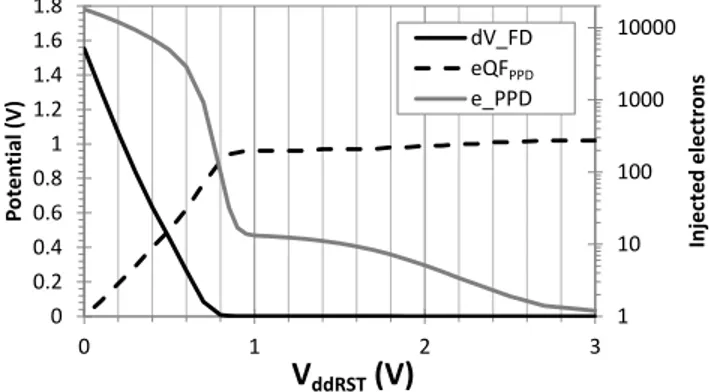
1 10 100 1000 10000 0 0.2 0.4 0.6 0.8 1 1.2 1.4 1.6 1.8 0 1 2 3 In ject e d e le ct ron s P ot e n ti a l (V )
V
ddRST(V)
dV_FD eQFPPD e_PPDFig. 3. TCAD simulation of the Vpinmeasurement. The voltage drop of the floating diffusion (dV FD) and the electron quasi Fermi level (eQFPPD) are reported on the left axis, and the amount of injected electrons in the PPD (e PPD) is reported on the right axis.
from the real device characterized in [11]. As it is generally the case, the PPD comprises the following layers, displayed in the Fig. 2:
• the N-PPD and the pinning P-PPD implantations
• the Pwell, isolating the circuitry from the bulk
• the N-plus layer, used for source or drain
• an anti-punch-through (APT), preventing leakage current
between the floating node and the PPD
• a Vt adjust layer avoiding the presence of a barrier
between the PPD and the APT layer
• a P-plus layer is used here as a ground contact (GND). All doping profiles were obtained by SIMS measurement, and the 2D device is created by Sentaurus Structure Editor. The gate spacers width is fixed at 80 nm. An additional doping profile is used on the reset transistor to adjust its threshold voltage.
B. Simulated test
The Vpinmeasurement is simulated with the same condition
as in II-B. After a reset of the PPD, electrons are injected in the PPD by means of a timing diagram similar to the one used in [8], [11]. At the end of this step, the number of injected electrons and the electron quasi Fermi potential in the PPD is read. Then, electrons are transferred in the reset floating node, and its potential is evaluated. This simulation sequence is performed for several VddRST between 0.0 V to 3.3 V. During
the electrical simulation, the following recombination models are activated in Sdevice: Auger, SRH(doping dependence) and Band2Band [17].
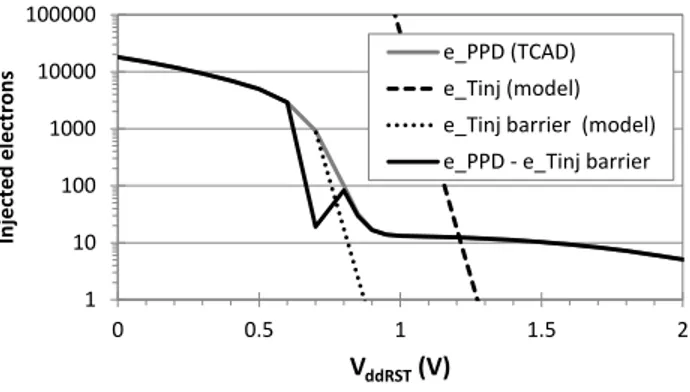
1 10 100 1000 10000 100000 0 0.5 1 1.5 2 In je ct e d e le ct ron s VddRST(V) e_PPD (TCAD) e_Tinj (model) e_Tinj barrier (model) e_PPD - e_Tinj barrier
Fig. 4. TCAD simulation of the Vpinmeasurement and analytical model of the thermionic injection without (e Tinj) and with potential barrier (e Tinj barrier). The curve e PPD-e Tinj barrier is the TCAD injected electrons in the PPD minus the thermionic injected electrons analytical model, which shows a quasi suppression of the exponential injection.
The Fig. 3 is showing the simulation result for the Vpin
measurement. As it can be seen, the simulated curve looks like the experimental one. At VddRST= 0 V, the voltage drop
of the floating diffusion is the highest, and it linearly decreases with the increase of VddRST until VddRST = Vpin ≈ 0.7 V.
For higher VddRST, almost no more charge is injected in the
PPD and the voltage drop remains flat. At VddRST = 0 V,
the electron quasi Fermi potential of the PPD is equal to 0.0 V because the PPD is at the Equilibrium Full Well Capacity (EFWC) [11], [18], and the amount of injected electrons is 18000. Then, between VddRST= 0.0 V and VddRST≈ 0.7 V,
the electron quasi Fermi level in the PPD (eQFPPD) linearly
increases as the amount of injected electrons decreases. And, between VddRST≈ 0.7 V and VddRST ≈ 0.9 V, the electron
quasi Fermi level still rises until eQFPPD = 1 V following
a different law. Indeed, in this regime the amount of injected electrons exponentially decreases until approximately a dozen of electrons. This particular regime is due to the presence of thermionic emission, which is an exponential function of the electrostatic barrier seen by electrons [19], [20]. Finally, between VddRST≈ 0.9 V and VddRST ≈ 3.0 V, the electron
quasi Fermi level slightly increases of 0.05 V and the number of injected electrons slightly decreases until the full depletion of the PPD. This last regime corresponds to the charge parti-tion regime, as menparti-tionned in [11]. Therefore, as concluded in [13], in TCAD simulation two different extractions of Vpin
may be done: the higher one (here, 0.9 V) gives the electron quasi Fermi level of the PPD when it is fully depleted as defined by Krymski [21], and the lower one (here, 0.7 V) is accessible experimentally, represents the electrostatic potential minimum of the PPD achieved when the depleted volumes contact. In the following, Vpinwill represent the lowest value,
accessible experimentally.
In the next part, the TCAD simulation and an analytical model are used to understand the mechanism at the origin of the thermionic injection.
C. Thermionic injection
1) Without barrier: Firstly, the thermionic injection is modeled without any potential barrier between the PPD and
the region under the TG. In this condition, it is supposed that the thermionic injection only occurs from the TG to the PPD when Vpin≥ Vinj. The amount of injected charge is then [20]:
Qth = KT2exp(−
q
kT(Vinj− Vpin)) × tinj (1) K = AR× Areainj , AR=
4πmqk2
h3 (2)
In this work Areainj is taken as 10 nm × 1 µm and
K ≈ 1.2 × 10⁻⁸ Am−2K−2. The Fig. 4 is showing the Vpin
measurement with the theoretical thermionic injected electrons using the calculated parameters for VddRST≥ 0.7 V. As it can
be seen, the amount of injected charge is much too high. In order to fit more suitable values, Areainj should be reduced
by seven orders of magnitudes. Consequently, the hypothesis ”without barrier” is unsuitable.
2) With barrier: A potential barrier φ is introduced between the PPD and the region under the TG. Electrons can go through this barrier from the TG and from the PPD. The amount of thermionic charge injected from the TG to the PPD is:
QthTG= KT2exp(−
q
kT(Vinj− Vpin+ φ)) × tinj (3) At first, the amount of thermionic charge injected from the PPD to the TG should be:
QthPPD= KT2exp(−
q
kTφ) × tinj (4)
However, compared to the reservoir of charge under the TG, the reservoir of charge in the PPD is extremely limited, because only few electrons have passed the barrier from the TG to the PPD. Therefore, the amount of electrons which can go through the barrier from the PPD to the TG must be balanced by a factor called here α, which depends on the amount of electrons located in the PPD:
QthPPD(α) = αKT2exp(−
q
kTφ) × tinj (5)
If the amount of charge in the PPD is high, or if QthTG is
high, the factor α has to approach 1.0. In opposition, if the amount of charge in the PPD is very low, or if QthTG is low,
the factor α has to approach 0.0. For this reason, the factor α is expressed as follows:
α = A × QthTG QthPPD
(6) where A is a constant.
The theoretical amount of thermionic injected electrons using an energetic barrier is displayed in the Fig. 4 (curve e Tinj barrier), by taking a barrier φ = 100 mV. By adjusting the A constant (in this work A = 0.9999928) it is possible to figure out the thermionic part of injected electrons. To illustrate it, the number of injected electrons in the PPD is plotted minus the thermionic injected electrons, and it can be seen that the exponential part of the injected electrons curve has disappeared. This shows that the thermionic injection is a bidirectional injection between the PPD and the TG around a small potential barrier.
To gain a better insight on how the thermionic injection occurs, the Fig. 5 is showing a potential diagram under three
V barrier PPD TG FD Vpin Vinj PPD TG FD Vpin Vinj thermionic emission PPD TG FD Vpin Vinj direct injection (a) (b) (c)
Fig. 5. Simplified electrostatic potential diagram of the PPD, TG, and FD for several injection bias conditions. (a) Vinjis too high, no thermionic injection. (b) Vinj≈ Vpin, bidirectional thermionic injection. (c) Vpin ≤ Vinj, direct injection. -5.E-19 -4.E-19 -3.E-19 -2.E-19 -1.E-19 0.E+00 0 0.1 0.2 0.3 0.4 P ot e n ti a l (e V) Cutline position (µm) =0.8V =0.7V =0.5V =3.3V VddRST VddRST VddRST VddRST TG FD Cutline Barrier
Fig. 6. TCAD simulation of potential under the TG when TG is ”ON”. A 2D electrostatic potential distribution is shown at VddRST = 0.7 V, and cutlines for 4 VddRST are displayed in the graph. In real reading mode, VddRST= 3.3 V.
conditions. Firstly (a), if VddRST is too high, no thermionic
injection is detectable. When VddRST is around Vpin (b) the
thermionic injection takes place and few electrons are injected in the PPD. Then, if VddRST≤ Vpinthe potential is lower than
the energetic barrier and electrons are linearly injected in the PPD (c).
This confirms that Vpin must not be extracted at the point
where the curve seems to meet the horizontal axis. Vpincan be
extracted from a linear extrapolation from the EFWC condition or by an integral extrapolation [11].
It is important to note that the potential barrier introduced in this part for the Vpinmeasurement does not affect the charge
transfer from the PPD to the floating node in a real reading mode. Indeed, as shown by the Fig. 6, the potential barrier is pulled toward the much higher floating node potential and no potential barrier is visible.
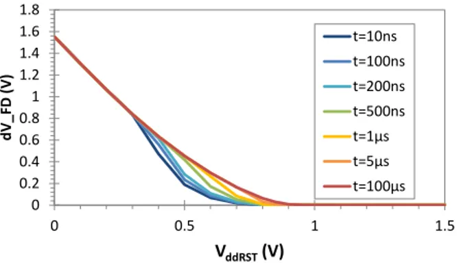
3) Influence of TG pulse duration: In order to check the reliability of the TCAD model with the thermionic injection, the simulation is performed with various TG pulse durations during the injection phase. According to experimental results, the longer the TG pulse duration, the higher the contribution of the thermionic injection is [11], because the thermionic emission is directly time dependent (see equation (1)). As it can be seen on the Fig. 7, for very short TG duration the thermionic injection becomes negligible. And, by increasing the TG pulse duration, the thermionic injection is more and more visible. This observation validates the TCAD simulation and the presence of thermionic injection.
D. Extracting a potential barrier from a curve shift
The potential barrier previously introduced does not affect the transfer from the PPD to the floating node in a reading
0 0.2 0.4 0.6 0.8 1 1.2 1.4 1.6 1.8 0 0.5 1 1.5 d V_FD (V) VddRST(V) t=10ns t=100ns t=200ns t=500ns t=1µs t=5µs t=100µs
Fig. 7. Vpin characteristics simulated for several TG pulse duration during the injection phase.
Reference Barrier on injection and reading Lower barrier on injection Higher barrier on injection QPPDbarrier
30
20
10
0
0
0.5
1.0
1.5
2.0
2.5
V
inj(V)
Q
out(e
-)
Fig. 8. Vpincharacteristics modified by the presence of a potential barrier during the injection mode and possibly in the reading mode. QPPDbarrieris the amount of electrons blocked in the PPD by the potential barrier.
mode. Let us suppose now that this potential barrier is strong enough and disturbs the PPD read-out. This could be the case if the bottleneck or the ”corridor” between the photodiode and the TG is long enough, creating an electrostatic barrier [11]. In this situation, the voltage at which the injection starts is reduced because of the presence of the potential barrier, and electrons remain in the PPD, causing Charge Transfer Inefficiency (CTI). Consequently, the Vpin curve is shifted to
the left (Fig. 8), and by knowing the PPD capacitance [11] it is then possible to calculate the height of the potential barrier:
QPPDbarrier =
Z Vbarrier
Vpin
CPPDdV (7)
where QPPDbarrier is the amount of electrons blocked in the
PPD by the potential barrier extracted from Fig. 8, Vbarrier
is the height of the potential barrier, and CPPD is the PPD
capacitance. In a similar way, other works mention a shift of the photon transfer curve because of a potential barrier under the TG which is present in the reading mode [22], [23]. Electrons remain in the PPD and cannot be transferred due to this potential barrier, and authors propose an extraction of their quantity from the curve shift.
As shown by Fig. 8, two kinds of potential barrier in the vicinity of TG may induce two different behavior on the Vpin
curve. If the barrier is present in injection and reading mode, it induces a curve shift and a higher CTI. If the barrier is
0 0.002 0.004 0.006 0.008 0.01 0.012 0 1 2 3 d V_F D (V) VddRST (V) Poly Silicium Poly Silicium Poly Silicium VddRST = 2.5V VddRST = 2.95V VddRST = 3.0V
Fig. 9. Zoom in of a simulated Vpin characteristic, and a selection of 2D electrons density distribution under the TG for VddRST= 2.5 V , VddRST= 2.95 V and VddRST = 3.3 V . TG inversion is visible for VddRST ≤ 2.95 V.
TABLE I
TCADEXTRACTION OF THETGINVERSION VOLTAGE FOR SEVERAL
VTGhigh.
VhighTG(V) 3.5 3.3 3.1 2.9 2.7 2.5 2.3
Vinv(V) 2.95 2.95 2.8 2.65 2.45 2.25 2.1
only present in injection mode, it influences the thermionic injection and should not increase the CTI.
E. Charge partition
Charge partition is an effect which is visible when Vpin≤
Vinj ≤ Vinv [11]. Indeed, when Vinj is below Vpin, an
inversion channel appears under the TG, and a charge partition mechanism between the PPD and the FD occurs when the TG is turned off. As a consequence, a plateau is visible in the Vpin
characteristic between Vpinand Vinv (Fig. 1). This plateau is
also visible in the TCAD simulation (see Fig. 9). Although this effect is well identified, extracting the TG inversion voltage from this curve is not obvious [12]:
• at the intersection of the Vpin characteristic with the
horizontal axis (at about 2.8 V in Fig. 9)
• at the end of the plateau (somewhere between 1 V and
2 V in Fig. 9)
To clarify this aspect, some TCAD pictures were recorded at several Vinj, TG being on. As shown by the Fig. 9, the
inversion channel is visible under the TG if VddRST is lower
than 2.95 V. Therefore, the TCAD simulation shows that the TG inversion voltage should be extracted at the intersection of the Vpincharacteristic with the horizontal axis. Further TG
in-version voltages are extracted for various VTGhighby means of
2D electron density TCAD pictures on the TG region. In this exercise, the high VTGvalue is changed from 3.3 V to other
VhighTG values, VlowTG remaining at 0.0 V. All the extracted
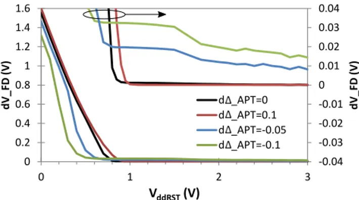
values are summarized in the Tab. I. Using the methodology proposed in [11], it is possible to estimate the channel doping level from the different inversion voltage extraction. An aver-age doping concentration of 4.0 × 10¹⁶at/cm3 is found from the values in the Tab. I, which is in a good agreement with the acceptor concentration used for the TCAD simulation (around 6.0 × 10¹⁶at/cm3). -0.04 -0.03 -0.02 -0.01 0 0.01 0.02 0.03 0.04 0 0.2 0.4 0.6 0.8 1 1.2 1.4 1.6 0 1 2 3 dV_FD (V ) dV_FD (V ) VddRST(V) d _APT=0 d _APT=0.1 d _APT=-0.05 d _APT=-0.1
Fig. 10. TCAD simulation of Vpincharacteristics of the PPD with variation on the anti-punch-through implantation (APT) position. A magnification of the characteristic shows a transfer of residual electrons which were not discharged in a previous reset of the PPD, commonly referred as lag.
IV. STUDY OF CONCEPTION ARTIFACTS:DEVELOPMENT
OF A DIAGNOSTIC TOOL
Once the TCAD model gives good confidence in reproduc-ing Vpin experiment and all the Vpincharacteristic behavior, it
can be used to study artifacts introduced by process or design parameters on the Vpincharacteristic. The aim is to elaborate
a diagnostic tool based on the comparison of the Vpin curve
with a reference one, which can help the designer to find a root cause of a possible problem on PPD design or process. With the aim of reaching this goal, three different conception modifications are introduced in the TCAD simulation, and their consequences are studied.
A. Modification of anti-punch-through implantation
In the first part, the anti-punch-through implantation posi-tion is modified around the reference posiposi-tion which is defined by the foundry. TCAD simulations of the Vpin measurement
are shown in the Fig. 10 for various shifts of the implantation. ∆APT ≤ 0 means that the implantation is moved in the
direction of the PPD, and ∆APT ≥ 0 means that it is shifted in
the opposite direction. As it can be seen, the closer to the PPD the implantation is, the lower the apparent Vpin is, the lower
the thermionic injection is, and the higher the lag is. The lag is identified by the amount of residual electrons not discharged in a previous PPD transfer and visible in the magnification of the curve in Fig. 10, as a potential deviation of the floating node due to the lag transfer. The reason is the increase of ”P” type doping between the PPD and the floating diffusion which leads to a higher potential barrier and a lower transfer quality. Thus, if the anti-punch-through implantation is too closed to the PPD, the whole curve is shifted, it shows a more pronounced drop before Vpin which prevents the right Vpin
extraction (Fig. 10). In opposition, moving away from the PPD the anti-punch-through implantation improves the transfer but may increase the parasitic collection of the floating node and its leakage current with the PPD.
Secondly, the anti-punch-through doping is changed. Simu-lations results are displayed in Fig. 11. Compared to the anti-punch-through shift, similar effects are visible on the Vpin
-0.04 -0.03 -0.02 -0.01 0 0.01 0.02 0.03 0.04 0 0.2 0.4 0.6 0.8 1 1.2 1.4 1.6 0 0.5 1 1.5 2 2.5 3 dV_FD (V ) dV_ FD (V ) VddRST(V) 140% APT 100% APT 67% APT 20% APT
Fig. 11. TCAD simulation of Vpincharacteristics of the PPD with variation on the anti-punch-through implantation (APT) doping. A magnification of the characteristic shows a transfer of residual electrons which were not discharged in a previous reset of the PPD, commonly referred as lag.
-0.2 0 0.2 0.4 0.6 0.8 1 1.2 1.4 1.6 1.8 0 0.5 1 1.5 2 2.5 3 d V_FD (V) N doped undoped P doped 0 0.001 0.002 0.003 0.004 0.005 0.5 1.5 2.5 dV_FD ( V) N doped 0 0.01 0.02 0.03 0.04 0.05 0.5 1.5 2.5 dV_FD ( V) P doped
V
ddRST(V)
VddRST (V) VddRST (V)Fig. 12. TCAD Vpin characteristic of the PPD with the reference N-doped TG, an undoped TG and a P-doped TG. A magnification of the characteristic shows the charge partition and the lag.
doping is, the higher the thermionic injection is. And the higher the doping is, the lower the apparent Vpin is, and the
higher the lag is. With a too high anti-punch-through doping, the potential barrier between the PPD and the FD is too high and the charge transfer is seriously affected. Moreover, as previously, Vpincannot be extracted.
To conclude, a too highly doped or a too closed APT implantation can be detected from the Vpin measurement.
Indeed, in this case, the PPD will have an important lag, and the Vpincurve will show a apparent reduced Vpinwith a
more pronounced drop before Vpin and almost no thermionic
injection.
B. TG doping
In this situation, the transfer gate doping is modified. Firstly, the gate is let undoped, as if the ”N” type doping implantation has been skipped. Secondly, the gate is ”P” doped. The Fig. 12 is showing the simulated results. With an undoped gate, the voltage drop across the gate becomes significant and the resulting potential difference at the bottom of the gate between the ”on” and the ”off” state is getting small. As a consequence, it is extremely difficult to transfer charge to and from the PPD, and the Vpin characteristic is strongly shifted to the
small VddRSTvalues. If the TG is ”P”-doped, the global Vpin
-0.04 -0.03 -0.02 -0.01 0 0.01 0.02 0.03 0.04 0 0.2 0.4 0.6 0.8 1 1.2 1.4 1.6 1.8 2 0 0.5 1 1.5 2 2.5 3 d V_FD (V) d V_FD (V) VddRST(V) 90% 100% 110%
Fig. 13. TCAD Vpin characteristic of the PPD with variation on the ”N” sensor implantation doping. 100% means the reference implantation doping. A magnification of the characteristic shows the charge partition and the lag.
characteristic looks similar to the reference one. However, if a magnification of the ”P”-doped characteristic closed to the horizontal axis is observed, it is possible to see a strong charge partition effect and a lower inversion voltage due to the TG ”P” type doping which decreases the flatband voltage. Moreover, resulting electrons attributed to the lag are also visible, because the ”P”-doped gate has lower flatband voltage and it is then more difficult to transfer efficiently electrons between the PPD and the floating diffusion.
Finally, an undoped gate can be detected with a Vpin
mea-surement because the apparent Vpinis abnormally low. A ”P”
doped gate can be identified by extracting an abnormally low TG inversion voltage, associated with a higher lag compared to the ”N” doped gate PPD.
C. NPDD doping
Finally the impact of the ”N” sensor doping concentration on the Vpincharacteristic is evaluated. As expected and shown
by the Fig. 13, a reduction of the ”N” sensor doping concen-tration leads to a shift of the Vpin curve to the left, because
Vpinand the EFWC are reduced. In opposition, a higher ”N”
sensor doping concentration increases the Vpin and therefore
the EFWC. For the smallest values of VddRST the simulation
shows a plateau, because of the saturation of the floating node. A higher ”N” sensor doping concentration also causes a higher lag because the PPD is more difficult to fully deplete.
Therefore, a change in the ”N” sensor doping concentration is also detectable by the Vpin measurement by means of the
curve shift. A higher doping should also induce a higher lag. D. Conclusion
To conclude this part, the TCAD simulations show that at least three kinds of conception anomalies can be detected by observing the Vpin characteristic. This study based on
simulations highlights which part of the Vpin characteristic is
affected by the anomaly, and it can be used as a diagnostic tool based on the observation of the pinning voltage measurement.
V. PPDIN REAL OPERATING MODE
As the simulated PPD is now verified and calibrated, a TCAD study of the PPD in its standalone mode is performed.
0 0.5 1 1.5 2 2.5 3 3.5 0.1 1 10 100 1000 10000
0.0E+00 2.0E-06 4.0E-06
V_T G (V ) e -in PP D Simulation time (s) 100% FD 71% FD 29% FD V_TG
Fig. 14. TCAD simulation of the PPD in a real reading mode. At t = 0, electrons are already injected in the PPD. After a reset phase, TG is ON at t = 2.1 µs and OFF at t = 4.2 µs, using a rise time and a fall time of 50 ns. Electrons stored in the PPD are monitored during the transfer phase for three floating diffusion sizes.
TG
PPD FD
V_TG=3.3V V_TG=1.65V V_TG=0.0V
100%FD
29%FD
Fig. 15. 2D TCAD electron density distributions around the TG during a real reading mode at the end of the transfer step and before TG is switched off (VTG= 3.3 V), at mid ramp (VTG= 1.65 V) and when TG reaches zero (VTG= 0.0 V). The reference PPD (100% FD) and the PPD with a reduced floating node (29% FD) are shown.
With the aim to study how the charge partition phenomena may occur in a PPD operated in real reading mode, the electrical simulation is modified. To do so, the injection phase using the reset transistor is suppressed in the timing diagram and replaced by an optical illumination. The illumination is characterized by a wavelength of λ = 700 nm and a power of 10 µW/cm2, which generates about 6600 electrons in the
PPD. The rising and falling times of the electrical commands are 50 ns and the plateau during the transfer phase is 2 µs long. The monitoring of electrons stored in the PPD during the transfer phase is displayed in the Fig. 14 for three floating node lengths:
• 100% of the reference length, as previously
• 71% of the reference length
• 29% of the reference length
If the floating diffusion is not reduced, all electrons stored in the PPD are transferred in the floating node, and no electrons are reinjected in the PPD when the TG is switched off. If the floating node area is reduced at 71% of the reference, its capacity is reduced and about one electron remains in the PPD because the floating node potential rises faster. At 29% of the reference area two electrons remain in the PPD at the end of the transfer plateau, and when TG is switched off more than three electrons are sent back in the PPD due to charge
0.01 0.1 1 10 100 1000 10000 100% FD 71% FD 29% FD e le ct r on s PPD_bef ramp PPD_mid ramp PPD_end ramp TG_bef ramp TG_mid ramp TG_end ramp
Fig. 16. TCAD simulation of the amount of electrons in the PPD or under TG at the end of the transfer step for three floating node sizes. The amount of electrons are shown before the falling ramp, at the half of the falling ramp, and at the end of the falling ramp.
partition.1
2D electron density pictures of the PPD with the highest and smallest FD are displayed in Fig. 15 at the end of the transfer step and before the falling ramp, at half of the falling ramp and at the end of the falling ramp. In addition, the amount of electrons integrated in the PPD and under the TG are reported in the Fig. 16 at the same time steps. When no charge partition is detectable in the simulation (100% FD and 71% FD), almost all electrons under the TG are transferred to the floating node before the half of the ramp down. In the PPD simulated with the smallest FD, a high amount of electrons under the TG is still not transferred to the floating node at the half of the falling ramp and the charge partition occurs in the last falling ramp part together with the transfer of the remaining electrons under TG.
This result shows that the charge partition mechanism may also occur in a PPD operated in a real reading mode, if the floating node is not sized correctly. Indeed, in this case, the floating node saturates before reaching the required FWC and electrons under the TG may go back to the PPD when TG is switched off. This mechanism occurs in the last part of the falling ramp of the TG, as a high amount of electrons has not been transferred to the floating node.
VI. CONCLUSION
TCAD simulations were conducted on a pinned photodiode in order to reproduced the pinning voltage measurement devel-oped by Tan [8]. TCAD results reproduce well experimental behaviors, and show the charge partition effect. By analyzing electrons distributions, these simulations have shown that the inversion voltage must be read at the intersection of the Vpin
characteristic with the horizontal axis. In addition, it was shown that a thermionic bilateral injection process occurs through a potential barrier at VddRST≥ Vpin.
By using this TCAD setup, conception artifacts were simu-lated in order to operate the Vpincharacteristic as a diagnostic
tool for PPD design or process issues, by comparing the reference measurement with the one showing one or several problems. Therefore, TCAD simulations have shown that a 40% more doped or a 50 nm too closed APT implantation can 1The same simulation was conducted with 300 electrons and did not show any spilled back electrons. It validates that the CTI is not degraded in the 29% FD device.
be detected thanks to an important lag, a Vpin curve showing
a apparent reduced Vpinwith a more pronounced drop before
Vpin and almost no thermionic injection. Then, an undoped
gate can be detected because the apparent Vpin is extremely
low. A ”P” doped gate can be identified by means of a lower TG inversion voltage, associated with a higher lag compared to the ”N” doped gate PPD. Finally, TCAD shows that a variation of 10% of PPD dose can be easily detected with Vpin measurements by observing a shift of the Vpincurve and
eventually a much higher lag for a higher ”N” sensor doping concentration.
The PPD was also simulated in a real reading mode, as it is used in an imager. The TCAD simulator has shown that the charge partition mechanism may also be present in this case, in particular if the floating node has a small capacity. In this situation, the charge partition occurs at the end of the falling ramp of the TG.
REFERENCES
[1] A. J. Theuwissen, “{CMOS} image sensors: State-of-the-art,” Solid-State Electronics, vol. 52, no. 9, pp. 1401 – 1406, 2008, papers Selected from the 37th European SolidState Device Research Conference -ESSDERC07.
[2] P. P. K. Lee, R. C. Gee, R. M. Guidash, T. h. Lee, and E. R. Fossum, “Active pixel sensor fabricated using cmos/ccd process technology,” in In Proceedings of IEEE Workshop CCD and Advanced Image Sensors, Dana Point, 1995.
[3] N. Teranishi, A. Kohono, Y. Ishihara, E. Oda, and K. Arai, “No image lag photodiode structure in the interline ccd image sensor,” in Electron Devices Meeting, 1982 International, vol. 28, 1982, pp. 324–327. [4] B. C. Burkey, W. C. Chang, J. Littlehale, T. H. Lee, T. J. Tredwell,
J. P. Lavine, and E. A. Trabka, “The pinned photodiode for an interline-transfer ccd image sensor,” in Electron Devices Meeting, 1984 Interna-tional, vol. 30, 1984, pp. 28–31.
[5] W. M. C. Sansen and C. J. M. Das, “A simple model of ion-implanted jfets valid in both the quadratic and the subthreshold regions,” IEEE Journal of Solid-State Circuits, vol. 17, no. 4, pp. 658–666, Aug 1982. [6] S. Park and H. Uh, “The effect of size on photodiode pinch-off voltage for small pixel cmos image sensors,” Microelectronics Journal, vol. 40, no. 1, pp. 137 – 140, 2009.
[7] A. Lahav, R. Reshef, and A. Fenigstein, “Enhanced x-ray cmos sensor panel for radio and fluoro application using a low noise charge amplifier wixel with a partially pinned pd,” International Image Sensor Workshop (IISW 2011), Hokkaido Japan, 2011.
[8] J. Tan, B. Buttgen, and A. J. P. Theuwissen, “Analyzing the radiation degradation of 4-transistor deep submicron technology cmos image sensors,” IEEE Sensors Journal, vol. 12, no. 6, pp. 2278–2286, June 2012.
[9] C. Y. P. Chao, Y. C. Chen, K. Y. Chou, J. J. Sze, F. L. Hsueh, and S. G. Wuu, “Extraction and estimation of pinned photodiode capacitance in cmos image sensors,” IEEE Journal of the Electron Devices Society, vol. 2, no. 4, pp. 59–64, July 2014.
[10] X. Yang, X. Ge, and A. J. Theuwissen, “Investigating transfer gate potential barrier by feed-forward effect measurement,” International Image Sensor Workshop (IISW 2015), Vaals Netherlands, 2015. [11] V. Goiffon, M. Estribeau, J. Michelot, P. Cervantes, A. Pelamatti,
O. Marcelot, and P. Magnan, “Pixel level characterization of pinned photodiode and transfer gate physical parameters in cmos image sen-sors,” IEEE Journal of the Electron Devices Society, vol. 2, no. 4, pp. 65–76, July 2014.
[12] Y. Xu, X. Ge, and A. J. P. Theuwissen, “A potential-based characteri-zation of the transfer gate in cmos image sensors,” IEEE Transactions on Electron Devices, vol. 63, no. 1, pp. 42–48, Jan 2016.
[13] A. Pelamatti, V. Goiffon, A. de Ipanema Moreira, P. Magnan, C. Vir-montois, O. Saint-P, and M. B. de Boisanger, “Comparison of pinning voltage estimation methods in pinned photodiode cmos image sensors,” IEEE Journal of the Electron Devices Society, vol. 4, no. 2, pp. 99–108, March 2016.
[14] A. Theuwissen, “Cmos image sensors: State-of-the-art and future per-spectives,” in Solid State Circuits Conference, 2007. ESSCIRC 2007. 33rd European, Sept 2007, pp. 21–27.
[15] N. Teranishi and N. Mutoh, “Partition noise in ccd signal detection,” IEEE Transactions on Electron Devices, vol. 33, no. 11, pp. 1696–1701, Nov 1986.
[16] L. Colquitt, Jr., N. Bluzer, and R. McKee, “Charge partition noise in charge-coupled devices,” Optical Engineering, vol. 26, no. 10, pp. 260 992–260 992–, 1987.
[17] Sentaurus Device User Guide, Synopsys, June 2015.
[18] A. Pelamatti, V. Goiffon, M. Estribeau, P. Cervantes, and P. Magnan, “Estimation and modeling of the full well capacity in pinned photodiode cmos image sensors,” IEEE Electron Device Letters, vol. 34, no. 7, pp. 900–902, July 2013.
[19] H. Bethe and M. I. of Technology. Radiation Laboratory, Theory of the Boundary Layer of Crystal Rectifiers, ser. Report (Massachusetts Institute of Technology. Radiation Laboratory). Radiation Laboratory, Massachusetts Institute of Technology, 1942.
[20] Y. Taur and T. H. Ning, Fundamentals of Modern VLSI Devices, 2nd ed. New York, NY, USA: Cambridge University Press, 2009.
[21] A. Krymski and K. Feklistov, “Estimates for scaling of pinned photodi-odes,” in Image Sensor Workshop, 2005.
[22] C. Chen, Z. Bing, W. Junfeng, and W. Longsheng, “Measurement of charge transfer potential barrier in pinned photodiode cmos image sensors,” Journal of Semiconductors, vol. 37, no. 5, p. 054007, 2016. [23] N. Teranishi, “The pinned photodiode,” in International Meeting on
Front-End Electronics, 2016.
Olivier Marcelot (M12) is a research scientist of physic of photodetector at ISAE. He got in 2007 a PhD Degree from the University Paul Sabatier of Toulouse, France. In 2008, he was working at Synopsys, as a development and application engineer. In May 2009, he joined Espros AG, Switzerland, as a device engineer. Since 2011, he is working in the integrated image sensor research team at ISAE.
Vincent Goiffon (S’08-M’09) received his M.S. (2005) and Ph.D. (2008) degrees in E.E. respectively from SUPAERO and Univ. of Toulouse. Since then, he has been working as an Associate Professor at ISAE-SUPAERO on CMOS image sensors design and characterization. He has co-authored more than 30 journal papers, including 1 Outstanding Conference Paper Award (NSREC) and 2 Outstanding Student Paper Awards (NSREC/RADECS).
Franck Nallet received his Ph.D. (2001) degrees in E.E. from INSA Lyon, on silicon carbide current limiting device. In 2002, he joined ISE TCAD in Zurich. Hes now working at SYNOPSYS Switzerland as application engineer manager, supporting Sentaurus TCAD users on many applications (process/device simulation, from high power devices up to nanowire-FET, as well as memories, TFT and CIS).
Pierre Magnan (M’99) graduated in E.E. from University of Paris in 1980. After being a research scientist involved in CMOS design up to 1993, he moved to image sensors research in ISAE, in Toulouse. He is currently full Professor there and Head of Image Sensor Research Group. He has co-authored more than 50 papers and a patent and served in IEDM DSM subcommittee in 2011, 2012, and in the IISW TPC in 2007, 2009, 2011.