To cite this version :
Pelamatti, Alice and Goiffon, Vincent and
Chabane, Aziouz and Magnan, Pierre and Virmontois, Cédric and
Saint-Pé, Olivier and Bréart-de-Boisanger, Michel
Speed Analysis
in Pinned Photodiode
CMOS
Image Sensors based on a Pulsed
Storage-Gate Method.
(2015)
In: Proceedings of European Solid-State Device conference
(ESSDERC), 15 September 2015 - 17 September 2015 (Gratz,
Austria).
O
pen
A
rchive
T
OULOUSE
A
rchive
O
uverte (
OATAO
)
OATAO is an open access repository that collects the work of Toulouse researchers and
makes it freely available over the web where possible.
This is an author-deposited version published in :
http://oatao.univ-toulouse.fr/
Eprints ID : 14562
Any correspondance concerning this service should be sent to the repository
administrator:
[email protected]
Charge Transfer Speed Analysis in Pinned
Photodiode CMOS Image Sensors based on a
Pulsed Storage-Gate Method
A. Pelamatti
∗, V. Goiffon,
∗, A. Chabane,
∗, P. Magnan,
∗C. Virmontois,
†, O. Saint-P´e,
‡, M. Breart de Boisanger
‡∗Institut Sup´erieur de l’A´eronautique et de l’Espace (ISAE), Universit´e de Toulouse,
Image Sensor Research Team, Toulouse 31055, France. Email: [email protected]
†Centre National d’Etudes Spatiales (CNES), Toulouse, 31400, France ‡Airbus Defence and Space, Toulouse, 31030, France
I. INTRODUCTION
D
RIVEN by low noise applications, Pinned Photodiode (PPD) [1]–[3] CMOS Image Sensors (CIS) have recently become the main image sensors technology for both commer-cial and scientific applications. The PPD (schematized in Fig. 1a) is formed by a double p-n junction, where the surface p+ implant, also referred to as pinning-implant, pins the surface at the substrate potential. This peculiar structure not only reduces the dark current (by isolating the collection buried channel from the charges generated at the SiO2-Si interface),but also limits the maximum PPD channel potential, often referred to as pinning voltage [4], which corresponds to the full depletion condition. The presence of this ”potential floor” enables true charge transfer from the PPD to the collection node (or to another buried channel), whereas in standard photodiodes (formes by a single p-n junction), only charge sharing between two capacitances is possible. The combination of these unique features has led in the last decade to the development of several PPD-based detectors for Time of Flight (ToF) applications [5]–[8], which require high speed readout of small packets of photo-charges. One of the main challenges involved in PPD-based high speed detectors is to reach the best time resolution by maximizing the charge transfer speed from the photo-generation site to the collection node. The transfer speed becomes even more critical for applications, such as space imaging applications, which require pixel pitches of several tens of µm (for example for optics-related constraints [9]).
In the last decade much effort has been put into improving charge transfer speed by introducing a drift field in the PPD [5], [7], [10]–[13] by modulating the PPD local potential. However the existing solutions often involve design and/or geometrical constraints, can require the use of a custom tech-nology, or might not be implementable for large pixel pitches (as the maximum potential difference which can be generated
The authors would like to thank CNES and Airbus Defence and Space for supporting the Ph.D of A. Pelamatti.
VG p-epi PMD p-well STI Pinned Photodiode (PPD) Floating Diffusion (FD) p-type pinning implant
Transfer Gate (TG) VDD_RST VDD ROW SELECT VPIX T3 T1 T2 RESET VFD n-type PPD implant Si VTG p-epi PMD p-well STI Pinned Photodiode (PPD) Floating Diffusion (FD) p-type pinning implant
Transfer Gate (TG) VDD_RST VDD ROW SELECT VPIX T3 T1 T2 RESET VFD n-type PPD implant Si Storage Gate (SG) VSG VTG VTG VFD PPD PPD (a) (b) (c) (d) LPPD WPPD LPPD=2/4/16/32µm WPPD=5µm VSG VFD
Fig. 1. Schematic cross-section (a) and top-view(b) of a typical PPD-based 4T active pixel. Schematic cross-section (c) and top-view (d) of the double gate structure used for the estimation of transfer time. The storage gate (SG) is used for storage (collection) and injection of charges, whereas the transfer gate (TG) enables charge transfer from the PPD to the floating diffusion (FD) as in standard PPD 4-T APS. LPPDis the PPD length and WPPD is the
PPD width.
within the PPD is equal to the pinning voltage, which is often of the order of 1V, or lower to ensure optimum charge transfer toward the floating diffusion). For these reasons, it is important
• to be able to predict whether speed performances in a
pure diffusion regime are sufficient or not for a target application (without the need of a custom design to
generate an electric field),
• to have a characterization method which allows to fairly assess transfer efficiency improvements for a given pixel design /potential modulation method.
Charge Transfer Inefficiency (CTI) curves have been simu-lated in [14], [15] for different PPD lengths by considering a uniformly distributed charge density. Experimental CTI measurements have also been shown in [15] for 16 µm pixels. However to the authors knowledge, no experimental study on the CTI has yet been shown for PPD lengths up to several tens of µm.
In this study we propose a new method to measure the charge transfer speed, which reproduces the ”worst-case sce-nario” of a ToF acquisition. This method is based on a double gate structure and is particularly suitable to compare the CTI for different pixel geometries as the measured transfer time is not affected by the initial distribution of charges in the PPD. It is also shown that the biasing voltage of the TG can strongly affect the CTI and that time constants involved in charge transfer can be of two order of magnitude higher than what is predicted by diffusion equations. This study also reports transfer speed data for PPD lengths up to 32 µm.
II. DEVICE UNDERTEST
A schematic drawing of the device tested in this work is shown in Fig. 1b. The device has been realized in a commercially available 0.18µm PPD CIS technology. The pixel structure is similar to a standard 4T active pixel sensor (APS), with an additional gate, referred to as Storage Gate (SG), which is used for the storage and release of charges. The transfer time has been measured for different PPD lengths: 2µm, 4µm, 16µm and 32µm. All PPDs are 5µm wide. The charge to voltage conversion factor (CVF) is about 10 µV/e− for all the tested pixels. The TG is 5µm wide and 0.7µm long. The storage gate size is 0.3µm × 5µm.
III. EXPERIMENTAL SET-UP
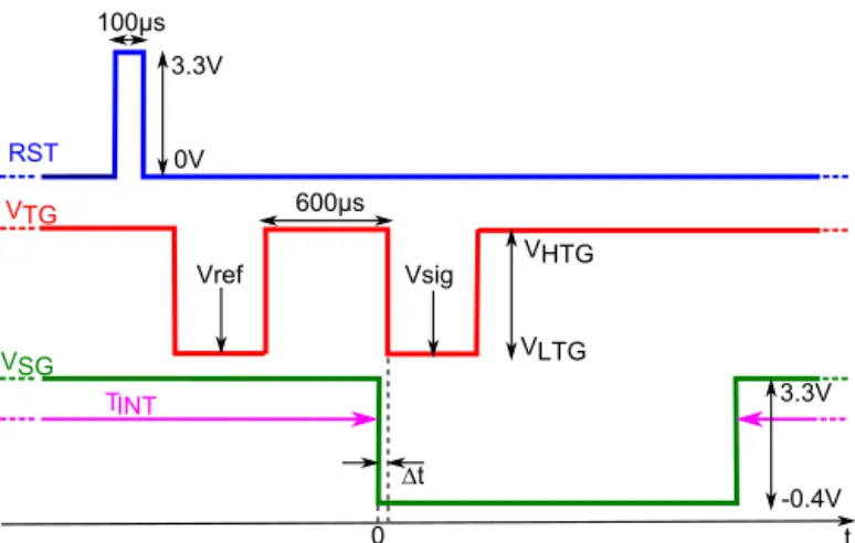
The proposed transfer time estimation method is based on the injection of charges at the opposite side of the PPD with respect to the TG at a given instant in time. In particular it consists in releasing the charge stored under the SG at a given instant before the closure of the TG. The timing diagram used in this paper is represented in Fig. 2: during the integration time, both the TG and the SG are ON (VSG = 3.3 V and
VTG = VHTG), thus charges generated in the PPD are either
stored under the SG, either drained toward the FD. At the beginning of the acquisition, the FD potential is reset to V DDRST for 100 µs (RST signal set to 3.3V) to empty
the PPD, then the TG is turned OFF (VTG = VLTG) to
sample the reference signal (Vref). Charge injection in the
PPD corresponds to the instant at which the SG is turned OFF (VSG= −0.4 V). The time delay ∆t between the falling
edges of the SG signal and the TG signal corresponds to the time during which charges can be transferred from the PPD to the FD. Once the TG is turned OFF, the signal (Vsig) is
∆t Vsig RST VTG VSG 600µs TINT 3.3V 0V Vref VHTG VLTG 3.3V -0.4V t 0 100µs
Fig. 2. Timing diagram for the proposed CTI estimation method
sampled. ∆t is increased from tens of ns to several hundreds of µs. The CTI is estimated as
CT I = 1 − Vsig(∆t) Vsig(∆tmax)
(1) where ∆tmax is the maximum tested delay, which must be
chosen long enough to ensure that all charges have been extracted from the PPD (100 µs here).
IV. FIRST RESULTS
Figure 3 shows the first results obtained with the proposed estimation method. Both the VTG and VSG signals vary
between 3.3V (pulse high level) and -0.4V (pulse low level). Data have been averaged over 1000 images and correspond to the output of single pixels (no spatial averaging is performed). Measurements have been obtained at room temperature in the dark. The integration time is 18 ms. Two main observations can be made based on these first results:
• The measured transfer time is almost 2 orders of magni-tude larger than the one estimated by numerically solving the diffusion equation1 and 1 order of magnitude larger
than the one measured in [15].
• As shown in Fig. 4, the transfer time (measured here as the time required to reach 0.01% CTI) increases as the square of the PPD length (except for the deviation at LPPD= 2 µm) as predicted by the diffusion equations. • Whereas the CTI is well fitted by an exponential curve at
LPPD= 32 µm, at shorter PPD lengths the CTI deviates
from the exponential behaviour for small time delays (at the beginning of charge transfer).
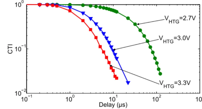
Figure 5 shows the CTI as a function of the SG-TG signals delay measured on a 16 µm long PPD for different TG biasing voltages (VHTG) during charge transfer . As it can be observed,
VHTGhas a strong influence on the CTI, thus despite the long
PPD length, diffusion is not the only phenomenon limiting
1The diffusion equation has been solved by assuming a perfect reflecting
wall and absorbing wall at x = 0 and x = LPPD, respectively. The starting
conditions correspond to a delta like charge density at x = 0 at t = 0. The diffusion coefficient has been set to Dn= 1.925 × 10⁻³m2/s
101 102 103 104 105 102 101 100 Delay (ns) C T I 32µm 16µm 4µm 2µm simulated CTI in a pure diffusion regime
for L
PPD=16µm
Fig. 3. Charge transfer inefficiency as a function of the time delay between the TG and SG signals (refer to chronogram in Fig. 2). The dashed curves correspond to the exponential fit of the experimental data (square markers).
0 5 10 15 20 25 30 35 40 0 10 20 30 40 50 LPPD(µm) T ra n sf e r ti me ( µ s ) Data y=ax2+b
Fig. 4. Transfer time corresponding to 0.001% CTI extracted from Fig. 3 as a function of LP P D: as it can be observed, for LPPD> 4µm the transfer
time increases with the square of the PPD length.
charge transfer speed. The important increase in transfer time with respect to the assumption of simple charge diffusion can be explained by the presence of a small potential barrier ( Fig. 6) at the PPD-TG interface (as suggested in [14]).
The CTI has been simulated for a 4 µm PPD in a pure diffusion regime, with and without the presence of a potential barrier Φb. Charge diffusion of charges has been simulated as
the random walk of 2500 single charges (Montecarlo simula-tion) located at x = 0 at t = 0−. The diffusion coefficient used in the simulation is about Dn= 1.925×10⁻³m2/s and charge
confinement within the PPD has been simulated by means of a perfect reflecting wall condition at x = 0. For the zero barrier simulation, a charge is considered to be transferred as soon it reaches x = LPPD. The effect of the potential barrier has
been taken into account by introducing the probability for a charge that reaches x = LPPD to have sufficient energy to
jump over the barrier [16]:
pjump= exp(−Φb/uth) (2)
with uth the thermal voltage. If the condition on the particle
energy is not satisfied, the potential barrier behaves as a reflecting wall. Electrostatic repulsion between charges has been neglected. As shown in Fig. 7, the presence of the
101 100 101 102 103 102 101 100 Delay (µs) C T I VHTG=2.7V V HTG=3.0V V HTG=3.3V
Fig. 5. CTI measured with the pulsed gate method on a 16 µm pixel for different TG biasing voltages during charge transfer (VHTG). Note that the
measured device is not the same as in Fig. 3, thus a small CTI difference is to be expected due to pixel to pixel variations.
FD
Fig. 6. Schematic potential diagram along the charge transfer path of the SG-PPD-TG-FD structure. The probability of a charge to be transferred from the PPD to the FD depends on the probability for the charge to have a sufficient energy to overcome the potential barrier [16] at the instant at which the charge is close to the potential barrier. The pinning voltage (Vpin) and the TG channel
potential (Vch) in Fig. 6 correspond to the values extracted in [17] and [18],
respectively
potential barrier Φb= 0.2 V can indeed increase the transfer
time of almost 2 orders of magnitude. A second effect which might play an important role in slowing down charge transfer is the bottle neck along the charge transfer path at the TG-PPD interface, which can also reduce the probability for charges to be transferred toward the FD.
V. CONCLUSIONS
In this work a new experimental method to extract the trans-fer time in a PPD based on specific test structures has been proposed. It has been shown, with the support of experimental data and numerical simulations, that simple charge diffusion might not be sufficient to model charge transfer (as it would lead to an important underestimation of the transfer time), thus thermionic emission of charges across the potential barrier at the TG-PPD interface should also be taken into account, even for long PPDs. On the basis of these first results, it can be inferred that introducing an electric field in the PPD can bring a double advantage with respect to a pure diffusion regimes,
101 100 101 102 103 102 101 100 Transfer Time (ns) C T I Random Walk, b=0.2V Random Walk, b=0V Diffusion, b=0V Effect of b
Fig. 7. Simulated CTI with and without considering a potential barrier Φb = 0.2 V at the TG-PPD interface. Charge diffusion is simulated by
the random walk of 1000 electrons (Montecarlo simulation). As it can be observed, the potential barrier can increase the transfer time of almost two orders of magnitude with respect to a pure diffusion regime. The dashed line is the CTI simulated by numerically solving the diffusion equation1.
as it would not only reduce the time required for the charges to cross the PPD, but it would also maintain charges close to the potential barrier, increasing the probability of jumping across the barrier. In this work only rectangular PPDs have been tested, however the proposed CTI extraction method can also be easily applied to other geometries to quantify the effect of the electric field on the transfer speed. The proposed method has two main advantages with respect to in-pixel CTI extraction methods [19]:
• It allows to compare the transfer speed for different geometries with equivalent initial conditions2.
• It reproduces a worst-case transfer time, when charges are photo-generated at the far end of the PPD with respect to the TG.
REFERENCES
[1] N. Teranishi, A. Kohono, Y. Ishihara, E. Oda, and K. Arai, “No image lag photodiode structure in the interline CCD image sensor,” in Electron Devices Meeting, 1982 International, vol. 28, 1982, pp. 324–327. [2] B. Burkey, W. Chang, J. Littlehale, T. Lee, T. Tredwell, J. Lavine, and
E. Trabka, “The pinned photodiode for an interline-transfer CCD image sensor,” in Electron Devices Meeting, 1984 International, vol. 30, 1984, pp. 28 – 31.
[3] E. Fossum and D. Hondongwa, “A Review of the Pinned Photodiode for CCD and CMOS Image Sensors,” Electron Devices Society, IEEE Journal of the, vol. 2, no. 3, pp. 33–43, May 2014.
2Whereas in typical CTI measurements, charges are not always equally
distributed in the PPD for different geometries (for example in square and trapezoidal photodiodes), thus the transfer speed can be artificially enhanced in trapezoidal PPDs (even if the PPD dimensions are too large to induce a non-negligible drift field) as charges are located (on average) closer to the TG.
[4] A. Krymski, N. E. Bock, N. Tu, D. Blerkom, and E. R. Fossum, “Estimates for scaling of pinned photodiodes,” in IEEE Workshop in CCD and Advanced Image Sensors, vol. 60, 2005.
[5] S.-M. Han, T. Takasawa, K. Yasutomi, S. Aoyama, K. Kagawa, and S. Kawahito, “A Time-of-Flight Range Image Sensor with Background Cancelling Lock-in Pixels Based on Lateral Electric Field Charge Modulation,” Electron Devices Society, IEEE Journal of the, vol. PP, no. 99, pp. 1–1, 2014.
[6] B. Buttgen, F. Lustenberger, and P. Seitz, “Demodulation Pixel Based on Static Drift Fields,” IEEE Transactions on Electron Devices, vol. 53, no. 11, pp. 2741–2747, Nov. 2006.
[7] C. Tubert, L. Simony, F. Roy, A. Tournier, L. Pinzelli, and P. Magnan, “High speed dual port pinned-photodiode for time-of-flight imaging,” in Proc. International Image Sensor Workshop, 2009, pp. 249–251. [8] S.-J. Kim, S.-W. Han, B. Kang, K. Lee, J. D. Kim, and C.-Y. Kim,
“A three-dimensional time-of-flight CMOS image sensor with pinned-photodiode pixel structure,” Electron Device Letters, IEEE, vol. 31, no. 11, pp. 1272–1274, 2010.
[9] S. Kraft, U. Del Bello, M. Drusch, A. Gabriele, B. Harnisch, and J. Moreno, “On the demands on imaging spectrometry for the monitoring of global vegetation fluorescence from space,” in Proc. SPIE, vol. 8870, 2013, pp. 88 700N–88 700N–12.
[10] H. Takeshita, T. Sawada, T. Iida, K. Yasutomi, and S. Kawahito, “High-speed charge transfer pinned-photodiode for a CMOS time-of-flight range image sensor,” in IS&T/SPIE Electronic Imaging, 2010, pp. 75 360R–75 360R.
[11] D. Durini, A. Spickermann, R. Mahdi, W. Brockherde, H. Vogt, A. Grabmaier, and B. J. Hosticka, “Lateral drift-field photodiode for low noise, high-speed, large photoactive-area CMOS imaging applications,” Nuclear Instruments and Methods in Physics Research Section A: Accelerators, Spectrometers, Detectors and Associated Equipment, vol. 624, no. 2, pp. 470–475, Dec. 2010.
[12] B. Shin, S. Park, and H. Shin, “The effect of photodiode shape on charge transfer in CMOS image sensors,” Solid-State Electronics, vol. 54, no. 11, pp. 1416–1420, 2010.
[13] X. Yang and A. Theuwissen, “Image Lag Analysis and Photodiode Shape Optimization of 4T CMOS Pixels,” in Proc. International Image Sensor Workshop, Jun. 2013.
[14] J. R. Janesick, T. Elliott, J. Andrews, J. Tower, and J. Pinter, “Funda-mental performance differences of CMOS and CCD imagers: part V,” in Proc. SPIE, vol. 8659, Feb. 2013, pp. 865 902–865 902.
[15] J. R. Janesick, T. Elliott, J. Andrews, J. Tower, P. M. Bell, A. Teruya, J. R. Kimbrough, and J. Bishop, “Mk x Nk gated CMOS imager,” in Proc. SPIE, vol. 9211, San Diego, California, United States, Aug. 2014. [16] P. Biljanovic and T. Suligoj, “Thermionic emission process in carrier transport in pn homojunctions,” in Electrotechnical Conference, 2000. MELECON 2000. 10th Mediterranean, vol. 1, 2000, pp. 248–251 vol.1. [17] A. Pelamatti, V. Goiffon, A. De Ipanema, P. Magnan, C. Virmontois, O. Saint-Pe, and M. Breart de Boisanger, “Absolute Pinning Voltage Measurement: Comparison between In-pixel and JFET Extraction Meth-ods,” in Proc. International Image Sensor Workshop, 2015.
[18] V. Goiffon, M. Estribeau, J. Michelot, P. Cervantes, A. Pelamatti, O. Marcelot, and P. Magnan, “Pixel Level Characterization of Pinned Photodiode and Transfer Gate Physical Parameters in CMOS Image Sensors,” Electron Devices Society, IEEE Journal of the, vol. 2, no. 4, pp. 65–76, Jul. 2014.
[19] L. Bonjour, N. Blanc, and M. Kayal, “Experimental Analysis of Lag Sources in Pinned Photodiodes,” IEEE Electron Device Letters, vol. 33, no. 12, pp. 1735–1737, Dec. 2012.