This is a publisher-deposited version published in:
http://oatao.univ-toulouse.fr/
Eprints ID: 4227
To cite this document:
GOIFFON Vincent, VIRMONTOIS Cédric, MAGNAN
Pierre, CERVANTES Paola, CORBIERE Franck, ESTRIBEAU Magali, PINEL
Philippe. Radiation damages in CMOS image sensors: testing and hardening
challenges brought by deep sub-micrometer CIS processes. In: SPIE Remote
Sensing, 20 - 23 Sept 2010, Toulouse, France.
Any correspondence concerning this service should be sent to the repository
administrator:
[email protected]
Radiation Damages in CMOS Image Sensors:
Testing and Hardening Challenges Brought by
Deep Sub-Micrometer CIS Processes
Vincent Goiffon, C´
edric Virmontois, Pierre Magnan, Paola Cervantes, Franck Corbi`
ere,
Magali Estribeau and Philippe Pinel
Universit´
e de Toulouse, ISAE, 10 avenue E. Belin, 31055, Toulouse, France
ABSTRACT
This paper presents a summary of the main results we observed after several years of study on irradiated cus-tom imagers manufactured using 0.18 μm CMOS processes dedicated to imaging. These results are compared to irradiated commercial sensor test results provided by the Jet Propulsion Laboratory to enlighten the differ-ences between standard and pinned photodiode behaviors. Several types of energetic particles have been used (gamma rays, X-rays, protons and neutrons) to irradiate the studied devices. Both total ionizing dose (TID) and displacement damage effects are reported. The most sensitive parameter is still the dark current but some quantum efficiency and MOSFET characteristics changes were also observed at higher dose than those of interest for space applications. In all these degradations, the trench isolations play an important role. The consequences on radiation testing for space applications and radiation-hardening-by-design techniques are also discussed. Keywords: CMOS image sensor, CIS, Active Pixel Sensor, APS, MAPS, pinned photodiode, deep submicrom-eter technology, DSM, ionizing radiation, total ionizing dose, TID, displacement damages, DDD, dark current, radiation-hardening-by-design, RHDB.
1. INTRODUCTION
Deep sub-micrometer (DSM) CMOS processes dedicated to imaging have brought important technological changes such as diodes dedicated to photodetection with optimized doping profiles and the introduction of trench isolations. These changes have a strong impact on the performances of CMOS imagers exposed to space radia-tion. In order to improve the radiation hardness of CMOS imagers for space applications, these new behaviors have too be identified and understood. Moreover, qualifying CMOS image sensors (CIS) for space applications also implies a good understanding of the basic effects.
In this paper we present a summary of the main results we observed after several years of study on irradiated custom imagers manufactured using 0.18 μm CMOS processes dedicated to imaging. These results are compared to irradiated commercial sensor test results provided by the Jet Propulsion Laboratory to enlighten the differ-ences between standard and pinned photodiode behaviors. Several types of energetic particles have been used (gamma rays, X-rays, protons and neutrons) to irradiate the studied devices. Both total ionizing dose (TID) and displacement damage effects are reported. The most sensitive parameter is still the dark current but some quantum efficiency and MOSFET characteristics changes were also observed at higher dose than those of interest for space applications. In all these degradations, the trench isolations play an important role. The consequences on radiation testing for space applications and radiation-hardening-by-design techniques are also discussed.
Further author information:
VDD RST ROW VDD 3T Pixel Collection node T1 T2 T3 Pixel output (a) (b) VDD RST ROW VDD 4T PPD Pixel Readout node TG T1 T2 T3 T4 Pixel output Floating diffusion (c) PPD TG FD C1 C2 (d)
Figure 1. CIS 3T and 4TPPD active pixel schematic and simplified top view illustration: (a) 3T pixel schematic, (b) 3T pixel top view illustration, (c) 4TPPD pixel schematic, (d) 4TPPD pixel top view illustration. PD stands for photodiode, CN stands for collecting node, FD for floating diffusion, RST for reset gate and TG for transfer gate.
2. BACKGROUND OVERVIEW AND EXPERIMENTAL DETAILS
2.1 Experimental details
All the results presented in this paper come from measurements performed on CISs (or test structures) manu-factured in deep submicron (0.18 μm) CMOS technologies dedicated to image sensors. If not stated otherwise, the measurement were performed at ISAE, at room temperature (≈ 22◦C) on three-transistor-per-pixel CMOS image sensors and test structures (10μm pixel pitch), all designed by ISAE. Pinned photodiode studies were conducted by the Jet Propulsion Laboratory on commercial sensors in the framework of the NASA electronic parts and Packaging (NEPP) Program.1
2.2 Specificities of image sensors manufactured using DSM CMOS technologies
Deep submicron CIS manufacturing processes (0.25 μm node and beyond) mainly differ from standard CMOS processes by the use of dedicated in-pixel doping profiles to enhance the photo-collection (by improving the quantum efficiency and by reducing the crosstalk) and to reduce the dark current (and noises). The dielectric stack is also often optimized to improve the light transmission to the pixel most sensitive area. Moreover, anti reflecting coating, micro-lenses and color filters are most often available in CIS processes and are widely used in commercial sensors. In comparison to older generation CIS processes, DSM CIS processes use trench isolations (most often shallow trench isolations (STIs)), thinner gate oxides and smaller transistors with several operating and threshold voltages. All these specificities change the behavior of irradiated CIS in comparison to the one studied in previous work.2–7 A few types of photodetectors are available in today’s DSM CIS technologies, and several elementary pixel architectures8 can be chosen as a starting point for a sensor design. Amongst these, we focus on the two following: the three-transistor-active-pixel (3T pixel) based on a classical P-N junction and the four-transistor-active-pixel with in pixel charge transfer (4TPPD pixel9) based on a fully depleted pinned
photodiode.10 Due to their capacity to perform in-pixel double correlated double sampling (CDS), their high
charge to voltage conversion factor and their extremely low dark current, 4TPPD pixels are widely used in small pitch commercial sensors. 3T pixels are still of interest for scientific applications, especially for large pitch sensors and for photon shot noise limited applications (in which the in-pixel CDS is not necessary). Indeed, pinned photodiodes available in DSM CIS technologies are usually optimized for small pixel pitches (below 4μm) and the use of in-pixel charge transfer for large pitches (more than 10μm) need to be studied more in detail. Moreover, 3T pixels can be designed in any CMOS technology, in contrary to 4TPPD pixels which require additional process steps.
These two elementary pixel architectures are presented in Fig. 1. In the 3T pixel (Fig. 1a), the transistor T1 is used to reset the photodiode at the beginning of the integration phase, T2 is used as a source follower amplifier and performs the charge to voltage conversion whereas T3 is used to access the pixel. In the 4TPPD version, transistors T1, T2 and T3 have the same functions than in the 3T architecture. However, the classical PN junction of the 3T pixel (Fig. 1b and Fig. 2a) is replaced by a pinned photodiode (Fig. 2b) and a transfer
N
P Space charge region Junction
Trench oxide Trench oxide
Pre-metal dielectric
(a)
N
P
Space charge region Junction
Trench oxide Trench oxide
Pre-metal dielectric
(b)
Figure 2. CIS pixel photodiode cross sections along C1. (a) 3T pixel and (b) 4TPPD pixel.
N P Transfer gate Trench oxide PMD Trench oxide N Floating diffusion Pinned photodiode
Figure 3. 4TPPD pixel cross section along C2, showing the
transfer gate. Figure 4. Radiation induced defects in MOS structures.
Trapped charges and interface states are generated by ion-ization whereas bulk defects are due to displacement dam-ages.
gate (Fig. 1d and Fig. 3)) used to transfer the charges collected in the pinned photodiode to the readout node, also called floating diffusion.
For the analysis of radiation induced degradation in CIS, it is very important to notice that in the 3T pixel, the depletion region ends at the trench oxide interface whereas it is confined in the bulk in the case of 4TPPD pixel.
2.3 Radiation induced damages in MOS devices
When passing through integrated circuits (ICs), particles from the space radiation environment11 deposit their
energy in two ways: by generating electron/hole pairs (ionization) or by displacing the atom nuclei (displacement damage). Cumulative ionization effects in ICs, usually called total ionizing dose (TID) effects,12, 13 are due to
electron/hole generation in IC dielectrics and can be directly induced by high energy photons (UV, X andγ-rays) and charged particles. TID is known to lead to two types of defects in dielectrics: trapped charges and interface states. The trapped charges are mainly trapped holes, often located near the Si/oxide interface. Interface states are dandling Si bonds which introduce energy states in the silicon band gap, at the interface. Displacement damages can be created in the silicon when a hadron (e.g. protons and neutrons) collides with a silicon nucleus and when the exchanged energy is sufficient to displace the Si atom from its original site, leaving a vacancy in the silicon lattice. Vacancies and displaced atoms often form stable defects by interacting with other vacancies or impurities. The resulting defects can be a point defect14 or a large combination of points defects, called cluster
of defects.15 Similarly to TID, the amount of energy a particle deposit in silicon by displacing atoms can be
quantified16, 17by the displacement damage dose (DDD).
Fig. 4 summarizes these radiation damages in MOS devices by showing that TID effects (trapped charges and interface states) are located in the IC oxides whereas displacement damages lead to bulk defects. In space applications, protons and electrons are the main sources of TID, but60Coγ-rays (1.17 and 1.33 MeV) are often
used to study ionization effects on-ground. Displacement damages effects in space applications are most often studied by using protons irradiations (which also induce TID effects).
Fig. 5 shows the measured trapped charge and interface state density evolutions with TID in a trench oxide of a CMOS image sensor. Both densities increase significantly with TID illustrating the build-up of trapped charges and interface states. These densities where extracted from current-voltage measurements on field-oxide FETs.18
100 101 102 103 1010 1011 1012 TID (krad) Δ N ot (cm −2 ) and Δ D it (cm −2 ⋅ eV −1 ) ΔDit ΔN ot
Figure 5. TID induced defect density increase in a CIS trench oxide (10 keV X-ray irradiations). NotandDitstand for trapped charge and interface state densities respectively.
-0.005 -0.004 -0.003 -0.002 -0.001 0 0.001 0.002 0.003 80 100 120 140 160 180 200 220 240 Temperature (K) Delta C /C Defect 2 (C-Oi) E = 0,33 eV Defect 3 (Bi-Oi) E = 0,28 eV Defect 1 (V²+) E = 0,18 eV Measurement : Bias : -5V Pulse : 0V Pulse width : 1e-3ms
Figure 6. DLTS spectrum measured on a large test photo-diode after neutron irradiation.
(a) (b) (c) (d)
Figure 7. CIS raw images (128x128 pixels). (a) dark image before irradiation (integration time = 2s). (b) dark image in the dark after 14 krad of TID (60Co, integration time = 400 ms). (c) dark image after 14 MeV neutron exposure (5× 1010cm−2, integration time = 2s). (d) image taken after 300 krad of TID (integration time = 8ms).
Fig. 6 shows a deep level transient spectroscopy (DLTS) spectrum measured on a CIS photodiode irradiated by 0.8 MeV neutrons (at a displacement damage dose of about 2 × 10¹⁰eV/g). It illustrates the generation of bulk defects induced by neutron in CISs.
3. RADIATION EFFECTS IN CIS
3.1 Degradation overview
The main degradation observed in irradiated image sensors manufactured in DSM CIS technologies is the overall dark current increase with TID19–23 which is usually uniform, but not always.24 As in older generation CISs,2, 6
the same problem arises in proton and neutron irradiated devices except that the dark current increase is not uniform.25 This is illustrated by the measurements summarized in Fig. 7. We can clearly see the differences
between the uniform dark current rise due to ionization in Fig. 7b and the generation of hot pixels due to displacement damages in Fig. 7c.
Fig. 8a shows the location of the radiation induced defects which play a role in the dark current increase in a 3T pixel photodiode. The TID induced defects responsible for the dark current increase are located in the depleted region, at the Si/oxide interface, as it is discussed in the next section. For displacement damage induced dark current, the responsible defects are also located in the space charge region, but throughout the depleted volume.
Other degradations have been reported in irradiated image sensors manufactured in CIS DSM technologies, such as wavelength dependent sensitivity drops,19, 21 maximum voltage output swing variation21 and noise in-crease.22 However all these effects appeared to be significant at TID much larger than the doses of interest for
N P SCR xxx + + + + + + + + + +xxx x +Trapped charge Interface state Bulk defect (a) N P SCR x x x x x x x x x x x x x x x x x x x x x x x x x x x x x x x x x x x x x x x x x x x x x x x x xx xx xInterface state Bulk defect (b)
Figure 8. Active defect in irradiated CISs. (a) Defects responsible for the radiation induced dark current increase. (b) Defects playing a role in the QE degradation.
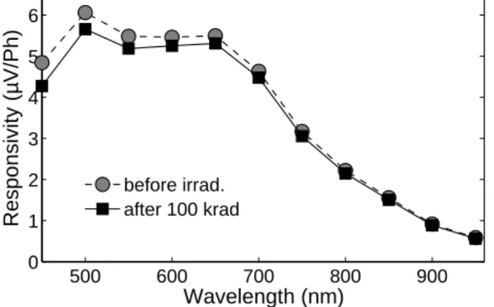
500 600 700 800 900 0 1 2 3 4 5 6 Wavelength (nm) Responsivity (µV/Ph) before irrad. after 100 krad
Figure 9. Mean responsivity of a 3T CIS before and after60Co irradiation (100 krad of TID).
typical space applications (> 50 krad). The fact that despite the dark current increase, the electrical parameters of the CIS do not change much with irradiation below≈ 100 krad is due to the intrinsic radiation hardness of DSM MOSFETs.
As regards the sensitivity, Fig. 8b shows how the radiation induced defects can degrade it. TID leads to sensitivity decrease at short wavelength (as illustrated in Fig. 9) by creating recombination centers at the Si/oxide interface. Only those located outside the depleted region play a significant role since the electric field in the space charge region sweep away the collected charge before they can recombine. But as mentioned just before, this effect is usually not a concern for typical space application TID. This seems even true for sensors which use micro-lenses21and for those who use micro-lenses and color filters.1
Displacement damages also induce the buildup of recombination centers in the silicon bulk, this could decrease the sensitivity for the longest wavelengths of the visible spectrum (by reducing the carrier lifetime and so the diffusion length). Nevertheless, no change has been observed after 1000 TeV/g of displacement damage dose. This is most likely due to the fact that the effective diffusion length of photo-generated carriers is already limited, before irradiation, by the thickness of the epitaxial layer used in the studied CISs. Displacement damage induced sensitivity drops could eventually become a problem in near infrared applications (in the case of frontside illumination) with a very thick epitaxial layer or with a lightly doped bulk wafer.
3.2 TID induced Dark current
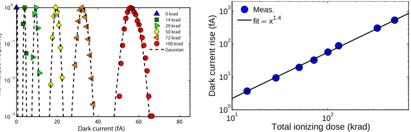
Typical radiation induced dark current distributions and mean increase are shown in Fig. 10 and 11. The degra-dation is pretty uniform as illustrated by the Gaussian shape of the dark current distribution after irradiation. It is interesting to notice that the relative non-uniformity (standard deviation divided by the mean) decreases with the exposure to ionizing radiations. Regarding the mean dark current, it increases monotonously with TID, suggesting that the cause of the degradation does not change in this TID range.
The radiation induced dark current increase can be expressed as the sum of two radiation induced contribu-tions:25
0 20 40 60 80 10−3
10−2 10−1 100
Dark current (fA)
Normalized frequency 0 krad 14 krad 29 krad 50 krad 72 krad 100 krad Gaussian
Figure 10. Dark current distribution of a 3T CIS for several TID (60Co irradiations). 101 102 100 101 102 103
Total ionizing dose (krad)
Dark current rise (fA)
Meas.
fit ∝ x1.4
Figure 11. CIS mean dark current increase as a function of TID (60Co irradiations). 0 0.01 0.02 0.03 0.04 0.05 0 0.02 0.04 0.06 0.08 0.1 0.12 P/S (µm-1) J (fA/µm²) Pre irrad 14 krad 29 krad 50 krad
Figure 12. Photodiode dark current density as a function of the perimeter over area ratio for several TIDs (60Co irradia-tions).
one proportional to the junction area Sj and the other to the junction perimeter Pj. This equation can be rewritten as follow: ΔJdark=ΔIdark Sj =JS+Pj Sj × JP . (2) This equation is plotted in Fig. 12 for several value of TID. In this case, the Y-intercept represents the area contribution, whereas the slope represents the perimeter contribution. It can clearly be seen that the perimeter contribution dominates for every studied Pj/Sj ratios. It must be emphasized that a Pj/Sj ratio of about 0.04 μm is a typical value for a scientific application. Such result indicates that the TID induced dark current comes from the perimeter of the junction, where the depletion region touches the STI interface. It has been shown18 that in these sensors, the radiation induced dark current was due to a classical Shockley-Read-Hall generation current (without any electric field enhancement26) which can be described by:
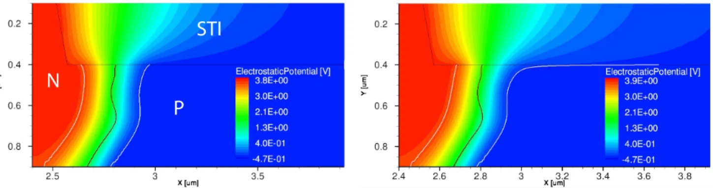
Idark(TID) =K · Pj· WSTI(ΔNot)· [Dit0+ ΔDit(TID)] , (3) withK a factor assumed independent of TID, WSTI the depletion width at the STI interface, ΔNotthe trapped charge increase with TID,Dit0 the interface state density before irradiation and ΔDit(TID) the interface state density increase with irradiation. This equation shows that both TID induced interface states and trapped charges play a role in the observed effect. Each interface state generated by the ionizing radiation act as an additional generation center which contributes to the overall dark current. As regards trapped charges, those located near the depletion region can extend the depletion width at the Si/oxide interface by changing locally the effective doping density.18 This effect is illustrated by the technology computer aided design (TCAD) simulations presented in Fig. 13 and Fig. 14.
N
P
STI
Figure 13. TCAD simulation showing the depletion region width at the Si/STI interface (right side of a 3T-pixel pho-todiode) before irradiation. The space charge region limits are represented by white lines.
Figure 14. TCAD simulation showing the depletion region width at the Si/STI interface after exposure to ionizing ra-diation (about 25 krad). The depletion region extension at the Si/STI interface can clearly be seen in this figure.
0 1 2 3 4 5
100
101
102
103
Total ionizing dose (krad)
Dark current (e−/s)
3T PD 2.2µm pitch 4TPPD 3.2µm pitch 4TPPD 2.2µm pitch
Figure 15. Comparison between 3TPD and 4TPPD dark current increases with TID. The 3T PD dark current plot comes from an extrapolation of the results presented in Fig. 11 on a 10 µm pixel pitch to a 2.2 µm pixel pitch. This interpolation is based on the direct proportionality be-tween the dark current and the junction perimeter in 3T pixel photodiodes. 0 1 2 3 4 5 0 2 4 6 8 10 12 14 16
Total ionizing dose (krad)
Relative dark current increase
3T PD 2.2µm pitch 4TPPD 3.2µm pitch 4TPPD 2.2µm pitch
Figure 16. Comparison between 3TPD and 4TPPD relative (according to eq. (4)) dark current increases with TID. The 3TPD dark current has been extrapolated to a 2.2 µm pixel pitch as detailed in the previous figure caption.
From these conclusions, the pinned photodiode appears to be the perfect photodetector to choose to avoid TID induced dark current. Indeed, since the depletion region does not touch the surrounding oxides (see Fig. 2b), this structure should be immune to TID induced dark current. Fig. 15 and 16 show that this is not the case. As a first approach, it can be seen in Fig. 15 that the absolute pinned photodiode dark current increase with TID is very small (more than two orders of magnitude lower) in comparison to the 3T pixel photodiode case. However, when the relative dark current increaseRDC
RDC= Idark|postirrad− Idark|prerad
Idark|prerad , (4)
is plotted as a function of TID (Fig. 16), we can see that the relative increase is comparable in the two cases. Worse, the presented data suggest an enhancement of the degradation at 5 krad, which has to be confirmed. The relative dark current increase can be more important for the application than the absolute increase since the instrument design is likely to be sized on the prerad performances. The exact origin of TID induced dark current in pinned photodiode is still under investigation.
Figure 17. Dark current distribution of proton and neutron irradiated CISs. 1.E-19 1.E-17 1.E-15 1.E-13
1.E-02 1.E-01 1.E+00 1.E+01 1.E+02 1.E+03 1.E+04 1.E+05 Displacement damage dose (TeV/g)
Dark current increase (A)
Measurements Displacement contributions
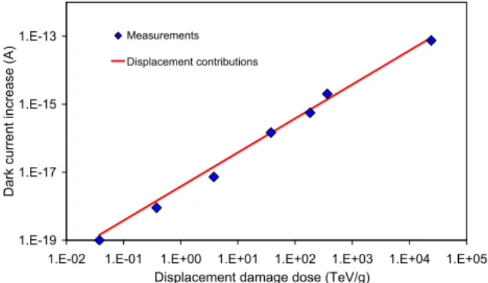
Figure 18. Mean dark current evolution with displacement damage dose in neutron irradiated CISs. The displacement damage contribution is estimated thanks to (5).
3.3 Displacement damage induced dark current
In contrary to TID, displacement damages in CISs lead to a non-uniform increase of the dark current by cre-ating hot pixels with very high dark current values. Fig. 17 shows the dark current distributions after proton and neutron irradiations with equivalent deposited displacement damage dose. After neutron beam exposure, ionization effects are negligible and the resulting distribution can be completely attributed to displacement dam-ages. One can clearly see in this figure and in Fig. 7c that displacement damages generate dark current extreme values distributed exponentially and most often called hot pixel tail. In contrary to what was observed in older technology based CIS,27 electric field enhancement was not observed in these sensors, even in the hot pixel tail. This pixel tail seems mainly due to the random nature of non-ionizing interaction in micro-volumes as it has been demonstrated in proton irradiated CCDs.28, 29 Recent work has confirmed this result in neutron irradiated
CISs,25 but further work is needed to completely model this hot pixel distribution tail.
At this displacement damage dose, we can see that no displacement damage has been created in the space charge region of most of the pixels. Indeed, no significant change can be seen on the Gaussian part of the neutron irradiated sensor distribution. This is not the case for the proton irradiated sensor distribution in which we clearly see a shift of the Gaussian part indicating that all the pixels have been degraded by the irradiation. This uniform degradation is due to the ionizing dose deposited by the proton flux, as shown in.25 Therefore, we
can conclude from this figure that proton irradiations are well representative of the space radiation environment, since it generates both ionizing and non-ionizing effects. However, the study of displacement damage effect alone is difficult in proton irradiated devices, and a deeper analysis can be done by studying neutron irradiated sensors. As regards the mean dark current increase due to displacement damage, previous work has shown that it is directly proportional to the displacement damage dose and to the photodiode depleted volume:17
ΔIdark =q · Vdep· Kdark· Dd , (5) withVdep the depleted volume,Dd the displacement damage dose andKdark the universal damage factor given in.17 Thanks to this equation, the mean dark current increase due to DDD can be predicted in any sensor as
far as the depleted volume is known. Note that if electric field enhancement26 appears in the depleted volume,
the previous equation must be corrected by an enhancement factor.27 Fig. 18 presents the application of the
universal damage factor concept to neutron irradiated CISs. One can see in this figure that the observed neutron induced mean dark current increase follows well the prediction based on (5) on the whole displacement damage dose range studied.
Because of the demonstrated universality of displacement damage effects in silicon photodetectors,17 the displacement damage induced dark current in pinned photodiode is expected to respect the universal damage factor concept. Therefore, for a given depletion volume, the dark current increase distribution following non-ionizing interaction will be the same in both types of sensors (3TPD and 4TPPD). Two main differences are however expected:
0 100 200 300 400 500 100 101 102 103 104 105
Dark current (e−/s)
Count (number of pixels)
Before irradiation
50 MeV proton, 12 TeV/g, 0.5 krad 50 MeV proton, 120 TeV/g, 5 krad Exponential tail fit
Figure 19. Dark current distribution in a commercial
2.2 µm-pitch-4TPPD sensor irradiated by 50 MeV protons
at 12 and 120 TeV/g. It corresponds to 3.2 × 10⁹ and
3.2 × 10¹⁰ protons/cm2. These distributions have been
re-produced from1 with permission.
0 10 20 30 40 50 60 1.5 2 2.5 3 3.5 4 Time (mn)
Dark current (fA)
Figure 20. Dark current random telegraph signal measured in a proton irradiated CIS.
• First, as the pre-radiation dark current is at least two orders of magnitude lower in pinned photodiodes
than in 3T pixel photodiodes, the relative dark current increase due to displacement damage will be one hundred times larger in pinned photodiode based sensors. This is especially true for the extreme dark current values.
• Second, high electric field regions are more likely to exist in pinned photodiodes (especially near the transfer
gate and the surface) than in a well designed 3T pixel photodiode. If displacement damages occur in such regions, the resulting dark current can be significantly enhanced.30
For these two reasons, displacement damage is expected to be a serious issue for the use of pinned photodiodes in space applications.
This discussion is illustrated by Fig. 19 which presents the dark current distribution of a pinned photodiode based sensor irradiated by protons for two displacement damage doses. One can notice that the hot pixel tail dark current values are very large in comparison to the very low pre-irrad dark current value (about 1 e−/s), even for the lowest displacement damage dose. The largest values, which are not shown in this figure for clarity purpose, are higher than 10000 times the prerad values.
In order to compare the hot pixel tail distribution generated in the pinned photodiode sensor and the one generated in the 3T sensor, the exponential slope of both distribution tails have been extracted. These slopes give an idea of the mean dark current induced by one non-ionizing interaction (assuming that most of the degraded pixels have undergone only one non-ionizing interaction in their depleted region). In the case of the 3T sensor (Fig. 17), the extracted slope is about 1 fA, which is five times the mean dark current before irradiation. In the case of the pinned photodiode sensor, the extracted slope is about 250 e−/s on the dark current range presented in Fig. 19. This gives a ratio of 250 between the prerad mean dark current and the estimated mean dark current per non-ionizing interaction. This ratio can goes up to 5000 if the whole hot pixel tail is taken into account. It clearly shows that displacement damage induced dark current extremes are much larger in pinned photodiode based sensors.
This result is not surprising. Indeed, in 3T pixel photodiode, the active defect density in the depleted region (mainly surface states) is already significant before irradiation. This is not the case in pinned photodiode where the dark current often seems dominated by the diffusion contribution. Hence, several generation centers must be created in the depleted region of a 3T pixel photodiode to induce a noticeable change in the dark current. On the contrary, a single generation center created in a pinned photodiode depletion region will generate a very large current compared to the initial value. The same phenomenon was observed in multi-pinned-phase CCDs compared to non-inverted CCDs (as discussed in31 p. 793).
The same effect can be expected regarding displacement damage induced dark current random telegraph signal32–34 (RTS) amplitudes (see Fig. 20 for an illustration of dark current RTS). Based on the assumption that the RTS defect density scales well will displacement damage dose35 and that the RTS mean amplitude is
not dependent on the technology nor on the depleted volume size (as suggested in36), much larger relative dark
current RTS amplitudes can be expected in pinned photodiode based CISs.
4. TESTING AND HARDENING-BY-DESIGN CHALLENGES
4.1 Remaining mysteries and testing issues
Regarding TID effects, most of the observed degradations come from the trench isolations. Further work is then needed to understand irradiated CIS trench oxide behaviors, especially after annealing. Indeed, trench oxide degradation evolution with annealing temperature and duration is hard to predict today (see for example the annealing results reported in18). Therefore, the behavior analysis of irradiated CISs after annealing can be very
difficult.
The origin of TID induced dark current in pinned photodiodes has to be clarified, and it would be useful to find techniques to properly discriminate the different dark current sources in pinned photodiode based pixels. There is also a strong need for radiation test methods (both for TID and DDD) dedicated to CIS that take into account CIS specificities, such as the particular behavior of irradiated trench oxides and their effect on the photodiode performances. Such methods should provide guidelines to correctly present the results to allow sensor-to-sensor comparison. For example, comparing the TID induced dark current in 3T-pixel photodiodes in nA/cm2 (photodiode dark current divided by the pixel area) does not seem very relevant since this current
is assumed to be proportional to the junction perimeter (and not to the pixel area). Regarding displacement damages, the use of neutron irradiations appears to be convenient to study displacement damage effects alone. It is worth mentioning that there is lack of criteria to clearly compare displacement damage effects in CISs, especially hot pixel distribution tails and random telegraph signals. Moreover, a physics based model to predict hot pixel tail in both 3T and 4TPPD pixels is still missing.
4.2 Radiation-hardening-by-design
Except small MOSFET leakage current increases,20 we haven’t seen any significant degradation of the analog and digital circuits in the space application radiation dose range. This is obviously due to the very good intrinsic radiation hardness of the MOSFETs manufactured in DSM CMOS technologies. In most of the cases, the slight MOSFET leakage current rise with TID is negligible, however it can become an issue in some particular sensors where the sensor performance is directly related to MOSFET off-state currents (e.g. when analog values must be stored for a long period of time, as in snapshot mode, or if this leakage is the main contribution to the power consumption). In such particular cases, the critical part of the circuit can efficiently be hardened by the use of enclosed layout transistors. In all other cases, MOSFET radiation hardening does not appear to be necessary for CIS dedicated to space applications. Regarding the use of P+ rings to mitigate inter device leakages, it seems
unnecessary since such leakages are not likely to appear below 100 krad.18, 20
To improve the sensor behaviors under irradiation, the efforts must be focused on improving the photodiode radiation hardness. This can be done in 3T pixel photodiode by changing the periphery of the PN junction as discussed in.37 However, no validated radiation hard photodiode layout (with systematic radiation hardness
improvement) compatible with any DSM CIS technology has been identified so far.
5. SUMMARY AND CONCLUSION
As far as we observed on the dose range applicable for space applications, ionization and displacement damage effects in imagers manufactured in DMS CIS technologies only lead to dark current increases. No degradation of digital circuits (even after 500 krad), no significant change in quantum efficiency, charge to voltage conversion factor and electrical gain was observed.
In the case of TID, the dark current increase was pretty uniform and it was attributed in 3T-pixels to the generation of interface states (and trapped charges) at the Si-oxide interface, in the photodiode depleted region.
This dark current is therefore directly proportional to the photodiode junction perimeter. In the case of pinned photodiode based pixels, the TID induce dark current increase is also important, especially when compared to the low pre-rad value. The exact cause of TID induced dark current in pinned photodiode is still under investigation. Displacement damage induced dark current distributions are non-uniform and non-ionizing interactions lead to the generation of hot pixel distribution tails in both types of sensors. The hot pixel dark current values are relatively much larger in the case of pinned photodiode based sensors than in the case of 3T-pixel sensors. Hence displacement damages in pinned photodiode based sensor appear to be a serious issue for their use in space applications.
Despite their very good intrinsic radiation hardness (functionality preserved after 500 krad of TID), much work is still needed to understand, model, predict and mitigate the dark current increases observed in irradiated CMOS image sensors manufactured in DSM CIS technologies.
ACKNOWLEDGMENTS
The authors are grateful to Cheryl Marshall (NASA GSFC) and Heidi N. Becker (JPL) for their help and for having provided the irradiated pinned photodiode data. The authors acknowledge the CNES, the CEA DAM DIF and EADS-Astrium for their support.
REFERENCES
1. H. N. Becker, J. W. Alexander, M. D. Dolphin, A. R. Eisenman, P. M. Salomon, L. E. Selva, and D. O. Thorbourn, “Commercial sensor survey fiscal year 2009 master compendium radiation test report,” tech. rep., Jet Propulsion Laboratory, 2009.
2. G. R. Hopkinson, “Radiation effects in a CMOS active pixel sensor,” IEEE Trans. Nucl. Sci. 47, pp. 2480– 2484, Dec. 2000.
3. M. Cohen and J.-P. David, “Radiation-induced dark current in CMOS active pixel sensors,” IEEE Trans.
Nucl. Sci. 47, pp. 2485–2491, Dec. 2000.
4. E.-S. Eid, T. Y. Chan, E. R. Fossum, R. H. Tsai, R. Spagnuolo, J. Deily, W. B. Byers, and J. C. Peden, “Design and characterization of ionizing radiation-tolerant CMOS APS image sensors up to 30 Mrd (Si) total dose,” IEEE Trans. Nucl. Sci. 48, pp. 1796–1806, Dec. 2001.
5. B. R. Hancock, T. J. Cunningham, K. P. McCarty, G. Yang, C. J. Wrigley, P. G. Ringold, R. C. Stirbl, and B. Pain, “Multi-megarad (Si) radiation-tolerant integrated CMOS imager,” in Proc. SPIE, 4306, pp. 147– 155, 2001.
6. J. Bogaerts, B. Dierickx, G. Meynants, and D. Uwaerts, “Total dose and displacement damage effects in a radiation-hardened CMOS APS,” IEEE Trans. Electron Devices 50, pp. 84–90, Jan. 2003.
7. B. Pain, B. R. Hancock, T. J. Cunningham, S. Seshadri, C. Sun, P. Pedadda, C. J. Wrigley, and R. C. Stirbl, “Hardening CMOS imagers: radhard-by-design or radhard-by-foundry,” in Proc. SPIE, 5167, pp. 101–110, 2004.
8. E. R. Fossum, “CMOS image sensors: electronic camera-on-a-chip,” IEEE Trans. Electron Devices 44, pp. 1689–1698, oct. 1997.
9. A. El Gamal and H. Eltoukhy, “CMOS image sensors,” IEEE Circuits and Devices Magazine 21, pp. 6–20, May - June 2005.
10. N. Teranishi, A. Kohno, Y. Ishihara, E. Oda, and K. Arai, “An interline CCD image sensor with reduced image lag,” IEEE Trans. Electron Devices 31, pp. 1829–1833, Dec. 1984.
11. E. G. Stassinopoulos and J. P. Raymond, “The space radiation environment for electronics,” Proc. IEEE 76, pp. 1423–1442, Nov. 1988.
12. T. P. Ma and P. V. Dressendorfer, Ionizing Radiation Effects in MOS Devices and Circuits, Wiley-Interscience, New York, 1989.
13. T. R. Oldham and F. B. McLean, “Total ionizing dose effects in MOS oxides and devices,” IEEE Trans.
Nucl. Sci. 50, pp. 483–499, June 2003.
15. B. R. Gossick, “Disordered regions in semiconductors bombarded by fast neutrons,” J. Appl. Phys. 30(8), pp. 1214–1218, 1959.
16. C. J. Dale, P. W. Marshall, G. P. Summers, E. A. Wolicki, and E. A. Burke, “Displacement damage equivalent to dose in silicon devices,” Appl. Phys. Lett. 54(5), pp. 451–453, 1989.
17. J. R. Srour and D. H. Lo, “Universal damage factor for radiation induced dark current in silicon devices.,”
IEEE Trans. Nucl. Sci. 47, pp. 2451–2459, Dec. 2000.
18. V. Goiffon, C. Virmontois, P. Magnan, S. Girard, and P. Paillet, “Analysis of total dose induced dark current in CMOS image sensors from interface state and trapped charge density measurements,” IEEE Trans. Nucl.
Sci. 57, Dec. 2010.
19. P. R. Rao, X. Wang, and A. J. P. Theuwissen, “Degradation of CMOS image sensors in deep-submicron technology due to γ-irradiation,” Solid-State Electron. 52, pp. 1407–1413, Sept. 2008.
20. V. Goiffon, P. Magnan, O. Saint-P´e, F. Bernard, and G. Rolland, “Total dose evaluation of deep submicron CMOS imaging technology through elementary device and pixel array behavior analysis,” IEEE Trans.
Nucl. Sci. 55, pp. 3494–3501, Dec. 2008.
21. V. Goiffon, M. Estribeau, and P. Magnan, “Overview of ionizing radiation effects in image sensors fabricated in a deep-submicrometer CMOS imaging technology,” IEEE Trans. Electon Devices 56, pp. 2594–2601, Nov. 2009.
22. R. E. Coath, J. P. Crooks, A. Godbeer, M. D. Wilson, Z. Zhang, M. Stanitzki, M. Tyndel, and R. A. D. Turchetta, “A low noise pixel architecture for scientific CMOS monolithic active pixel sensors,” IEEE Trans.
Nucl. Sci. , 2010.
23. P. Vu, B. Fowler, B. Rodricks, J. Balicki, S. Mims, and W. Li, “Evaluation of 10MeV proton irradiation on 5.5 Mpixel scientific CMOS image sensor,” in Proc. SPIE, 7826(60), 2010.
24. B. Dryer, A. Holland, N. J. Murray, P. Jerram, M. Robbins, and D. Burt, “Gamma radiation damage study of 0.18 m process CMOS image sensors,” in Proc. SPIE, 7742, 2010.
25. C. Virmontois, V. Goiffon, P. Magnan, S. Girard, C. Inguimbert, S. Petit, G. Rolland, and O. Saint-Pe, “Displacement damage effects due to neutron and proton irradiations on CMOS image sensors manufactured in deep sub-micron technology,” IEEE Trans. Nucl. Sci. 57, Dec. 2010.
26. G. Vincent, A. Chantre, and D. Bois, “Electric field effect on the thermal emission of traps in semiconductor junctions,” J. Appl. Phys. 50(8), pp. 5484–5487, 1979.
27. J. Bogaerts, B. Dierickx, and R. Mertens, “Enhanced dark current generation in proton-irradiated CMOS active pixel sensors,” IEEE Trans. Nucl. Sci. 49, pp. 1513–1521, June 2002.
28. P. Marshall, C. Dale, E. Burke, G. Summers, and G. Bender, “Displacement damage extremes in silicon depletion regions,” IEEE Trans. Nucl. Sci. 36, pp. 1831–1839, Dec. 1989.
29. P. Marshall, C. Dale, and E. Burke, “Proton-induced displacement damage distributions and extremes in silicon microvolumes charge injection device,” IEEE Trans. Nucl. Sci. 37, pp. 1776–1783, Dec. 1990. 30. J. R. Srour and R. A. Hartmann, “Enhanced displacement damage effectiveness in irradiated silicon devices,”
IEEE Trans. Nucl. Sci. 36, pp. 1825–1830, Dec. 1989.
31. J. Janesick, Scientific Charge-Coupled Devices, SPIE Press, 2001.
32. I. H. Hopkins and G. R. Hopkinson, “Random telegraph signals from proton-irradiated CCDs,” IEEE Trans.
Nucl. Sci. 40, pp. 1567–1574, Dec. 1993.
33. I. H. Hopkins and G. R. Hopkinson, “Further measurements of random telegraph signals in proton-irradiated CCDs,” IEEE Trans. Nucl. Sci. 42(6), pp. 2074–2081, 1995.
34. J. Bogaerts, B. Dierickx, and R. Mertens, “Random telegraph signal in a radiation-hardened CMOS active pixel sensor,” IEEE Trans. Nucl. Sci. 49, pp. 249–257, Feb. 2002.
35. G. R. Hopkinson, V. Goiffon, and A. Mohammadzadeh, “Random telegraph signals in proton irradiated CCDs and APS,” IEEE Trans. Nucl. Sci. 55, Aug. 2008.
36. V. Goiffon, G. R. Hopkinson, P. Magnan, F. Bernard, G. Rolland, and O. Saint-Pe, “Multilevel RTS in proton irradiated CMOS image sensors manufactured in a deep submicron technology,” IEEE Trans. Nucl.
Sci. 56, pp. 2132–2141, Aug. 2009.
37. B. Hancock and G. Soli, “Total dose testing of a CMOS charged particle spectrometer,” IEEE Trans. Nucl.