an author's https://oatao.univ-toulouse.fr/22819
http://doi.org/10.1109/TNS.2018.2884037
Rizzolo, Serena and Goiffon, Vincent and Corbière, Franck and Molina, Romain and Chabane, Aziouz and Girard, Sylvain and Paillet, Philippe and Magnan, Pierre and Boukenter, Aziz and Allanche, Timothé and Muller, Cyprien and Monsanglant-Louvet, Celine and Osmond, Melanie and Desjonquères, Hortense and Macé, Jean Reynald and Burnichon, Pierre and Baudu, Jean-Pierre and Plumeri, Stéphane Radiation Hardness Comparison of CMOS Image Sensor Technologies at High Total Ionizing Dose Levels. (2019) IEEE Transactions on Nuclear Science, 66 (1). 111-119. ISSN 0018-9499
Radiation Hardness Comparison of CMOS Image
Sensor Technologies at High Total
Ionizing Dose Levels
Serena Rizzolo , Vincent Goiffon , Franck Corbière, Romain Molina, Aziouz Chabane, Sylvain Girard ,
Philippe Paillet , Pierre Magnan, Aziz Boukenter, Timothé Allanche , Cyprien Muller ,
Céline Monsanglant-Louvet, Mélanie Osmond, Hortense Desjonquères, Jean-Reynald Macé,
Pierre Burnichon, Jean-Pierre Baudu, and Stéphane Plumeri
Abstract— The impact of the manufacturing process on the radiation-induced degradation effects observed in CMOS image sensors (CISs) at the MGy total ionizing dose (TID) levels is investigated. Moreover, the vulnerability of the partially pinned PHDs at moderate-to-high TIDs is evaluated for the first time to our knowledge (PHD stands for “photodiode”). It is shown that the 3T-standard partially pinned PHD has the lowest dark current before irradiation, but its dark current increases to
∼1 pA at 10 kGy(SiO2). Beyond 10 kGy(SiO2), the pixel func-tionality is lost. The comparison between several CIS technologies points out that the manufacturing process impacts the two main radiation-induced degradations: the threshold voltage shift of the readout chain MOSFETs and the dark current increase. For all the tested technologies, 1.8-V MOSFETs exhibit the lower threshold voltage shift, and the nMOSFETs are the most radiation tolerant. Among all the tested devices, 1.8-V sensors achieve the best dark current performance. Several radiation-hardening-by-design solutions are evaluated at the MGy level to improve further the understanding of CIS radiation hardening at extreme TID.
Index Terms— CMOS image sensors (CISs), dark current, drain, gate overlap, partially pinned PHD, radiation effects, radiation hardening by design (RHBD), threshold shift, total ionizing dose (TID).
I. INTRODUCTION
C
MOS image sensors (CISs) are today the main solid-state imaging technology and are widely used for the development of scientific applications associated with radia-tion environments [1], [2].Manuscript received November 6, 2018; revised November 26, 2018; accepted November 26, 2018. Date of publication November 29, 2018; date of current version January 17, 2019.
S. Rizzolo, V. Goiffon, F. Corbière, R. Molina, A. Chabane, and P. Magnan are with ISAE-SUPAERO, Université de Toulouse, 31055 Toulouse, France (e-mail: serena.rizzolo@isae.fr).
S. Girard, A. Boukenter, and T. Allanche are with the Laboratoire Hubert Curien, UMR-CNRS, Université de Lyon, 42000 Saint-Étienne, France.
P. Paillet is with DIF, DAM, CEA, 91680 Arpajon, France.
C. Muller is with the Laboratoire Hubert Curien, UMR-CNRS, Université de Lyon, 42000 Saint-Etienne, France, and also with DIF, DAM, CEA, 91680 Arpajon, France.
C. Monsanglant-Louvet, M. Osmond, and H. Desjonquères are with the Centre de Saclay, IRSN, 91192 Gif-sur-Yvette, France.
J.-R. Macé is with Orano, 92400 Paris, France.
P. Burnichon and J.-P. Baudu are with Optsys, 42000 Saint-Étienne, France. S. Plumeri is with Andra, 92290 Châtenay-Malabry, France.
Fig. 1. Pixel cross-sectional view of (a) typical 3T pixel and (b) surface-protected 3T pixel [3]. (c) Cross-sectional view of typical 3T partially pinned PHD pixel. (d) Cross-sectional view of a typical pinned PHD (also called 4T pixel). SCR= space charge region. RST = reset MOSFET.
Space remote sensing, medical imaging but also nuclear and high energy physics applications require the use of imaging systems able to withstand dose levels up to the MGy(SiO2)
(1 MGy = 100 Mrad) range. Tube-type cameras offer the highest radiation hardness today but they are fragile and voluminous, and both their performance and reliability are limited. Commercially available off-the-shelf radiation tolerant cameras based on solid-state image sensors, such as charge injection devices or CIS, are limited to a maximum total ion-izing dose (TID) of 100 kGy(SiO2) [4], [5]. Goiffon et al. [6]
has demonstrated that optimized radiation-hardened CISs can withstand TID up to 10 MGy(SiO2). It has been shown
thatradiation-hardening-by-design (RHBD) solutions such as the use of 1.8-V nMOSFET and pMOSFET or the exclusive use of N transistors for CIS readout chain reduce the threshold voltage shift induced by TID, thus improving the dynamics of the sensors itself. Moreover, optimized pixel design architec-tures have been proposed to reduce the dark current increase with radiation dose [6].
This study is placed in the framework of the CAMRAD Project which looks to develop and test, under real conditions, a high-performance (color camera, high sensitivity, and high resolution) imaging system that could withstand TID > 1 MGy(SiO2) for the characterization and monitoring of
nuclear waste, the maintenance, and instrumentation of nuclear facilities.
The purpose of this paper is to study, through the compar-ison of several CIS technologies, the impact of the manufac-turing process on the two main radiation-induced degradations observed at the MGy TID levels: MOSFETs’ degradation and dark current increase. The objective is to evaluate the role of the CIS technology in the radiation hardness process in order to establish if equal pixel designs which differ only from the manufacturing process lead to different radiation responses. Moreover, thanks to various pixel designs, an investigation of diverse photodiode (PHD) solutions is carried out to study, for the first time to our knowledge, the radiation hardness of the partially pinned PHD. A new variant of the gate overlap design proposed in [6] and analyzed through the TCAD simulation in [7] is for the first time characterized. The response of several RHBD pixel variants based on the gate overlap pixel is investigated to better understand their potential and limits and to improve the radiation hardness of CIS for high TID applications.
II. OVERVIEW OF THESTANDARDCIS PHOTODIODES
Different types of PHDs used in CIS are illustrated in Fig. 1. The 3T-standard PHD, Fig. 1(a), is composed of a pho-tosensitive region, the n-doped PHD, and three transistors to reset the signal (RST), to amplify it [source follower (SF) transistor], and to select the row [row select (RS) transistor] to the column readout chain [1]. In this PHD, the depleted region reaches the Si/SiO2 interfaces associated with the shallow
trench isolation (STI) or with the premetal dielectric (PMD). Hence, all the defects present in the oxide that are in contact with the n-region can contribute to the dark current [2]. This PHD has been widely evaluated under radiation. It is reported that STI positive trapped charges lead to a short circuit between pixels with a consequent change of the PHD capacitance [8]–[10].
A variant of this PHD described in [3] and fabricated to improve the radiation hardness is illustrated in Fig. 1(b). It consists of a 3T pixel where the top is covered with a p+ implant which reduces the dark current by reducing the contact area between the PHD depletion region and the surrounding oxides (STI and PMD). As shown in Fig. 1(a), in this pixel, called surface-protected PHD, the n-region is not depleted. It has been shown that this optimized p+ layer enhances the dark current performances with respect to the 3T pixel for low-to-moderate TID levels [3].
Fig. 1(c) depicts the 3T-standard partially pinned PHD [11], [12], never investigated under irradiation to the best of our knowledge. Also, in this particular PHD, the top of the n-doped region is covered with a p+ implant to prevent the contact between the depletion region and the oxides. In this case, as shown in Fig. 1(c), the PHD depth is reduced in order to fully deplete the PHD during
TABLE I
CIS CHARACTERISTICS’ OVERVIEW
the operation [12]. In order to connect the PHDs shown in Fig. 1(b) and (c) to RST MOSFET, the p+ pinning layer has to be opened somewhere to let the n-region reach the surface. Therefore, in surface-protected and partially pinned PHDs, the depletion region is in contact with oxide interfaces, in the vicinity of the RST contacts. Since the total area of the depleted oxide interface is smaller than in a standard 3T pixel, the dark current is lower in these PHDs than in a 3T pixel.
Finally, the pinned PHD, used in 4T pixels, is shown in Fig. 1(d). In pinned PHD, an additional MOSFET, i.e., the transfer gate TG, is needed to transfer the charge between the pinned PHD and the sense node. Pinned PHD exhibits the best dark current performances before irradiation, since the p+ pinning layer prevents the contact between the PHD and the oxides. However, it has been shown in [13]–[15] that the pinned PHD suffers from severe degradation due to TID, such as charge transfer degradation and dark current increase because of the trapped charges in the PMD and in the spacers. Since no RHBD solutions can be proposed to improve the radiation hardness of pinned PHD at high TID, the 4T PHDs are not investigated in this work. This study is indeed devoted to the evaluation at TID up to 1 MGy(SiO2) of standard 3T
PHD, standard 3T partially pinned PHD, and RHBD solution based on gate overlap 3T PHD. Several design variants of the gate overlap PHD are presented and evaluated, differing in the pixel-to-pixel isolation (e.g., STI, gate, and STI + gate) as well as in a new technique based on the addition of an n+ drain in the gate overlap pixel.
III. EXPERIMENTALDETAILS
To carry out this study, four CIS were manufactured using two different 180-nm CIS processes with dedicated and opti-mized in-pixel devices. A comparison with a third technology is performed, thanks to the results available in [6].
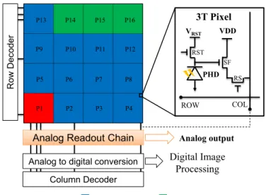
The architecture of the studied CISs is presented in Fig. 2. The integrated image sensors for each technology are com-posed of a pixel array (128× 256 or 256 × 256 pixels each array) with three transistors per pixel (see Fig. 3). For this exploration, sequencing and analog-to-digital conversion are realized off-chip. The pixel array and the analog readout circuits are designed using both a mixed 3.3- and 1.8-V nMOSFET and pMOSFET and a full 1.8-V nMOSFET and pMOSFET in order to evaluate the radiation hardness of each solution. All the transistors of the readout chain have been radiation hardened by ISAE-SUPAERO using enclosed layout transistors [16] to mitigate the radiation-induced narrow channel effects and sidewall leakage [17]. Table I summarizes the characteristics of each sensor.
Fig. 2. Architecture of the studied CIS showing the overview of the investigated pixel designs (see Table II for details). All the pixels are composed of the PHD and three transistors to reset the voltage of the PHD (RST MOSFET), to amplify the signal (SF MOSFET) and to select the row (RS MOSFET). The integrated circuit is constituted of the pixel array and the analog readout chain, whereas the digital conversion and line and column decoders are off-chip.
Pixel arrays have been divided into 16 regions to investigate the radiation hardness of diverse pixel designs and RHBD solutions. The comparison between the 3T-standard [see Fig. 1(a)] and the 3T-standard partially pinned PHDs [illus-trated in Fig. 1(b)] allows studying the radiation hardness of the partially pinned design at both kGy and MGy TID levels. As summarized in Table II, different RHBD solutions based on the gate overlap design (P2) are investigated. This design, illustrated in Fig. 3(a), is the typical gate overlap design of [6]. In particular, for this study, the impact of the overlap region
d [see Fig. 3(e) and (f)] is investigated, thanks to pixels P2–P4.
Another important point was to study the influence of the pixel-to-pixel isolation, in which the gated overlap design of P2 is realized only by the gate. This could lead to short circuits between the PHDs in several situations, e.g., high contrast images. To avoid the short circuit, in some designs (see for example P5 in Table II), the intrapixel isolation is realized by the STI and the polysilicon gate.
The comparison between the two thicknesses of the gate oxide (double GO2 and simple GO1) is evaluated, thanks to the pixel P6 in the 3.3-V CISs. The new variants of the gate overlap pixel investigated in this paper are presented in Fig. 3(b)–(d). In these designs (pixels P8–P13 of Table II), an n+ drain (biased at VDD) is added in order to enhance the dark charges draining mechanism observed for high TID (>0.1 MGy) when a positive voltage is applied to the gate [6]. As listed in Table II and depicted in Fig. 3(b)–(d), several variants of this pixel-type differing in the size of the n+drain and in the pixel isolation, are taken into consideration in this study.
Room temperature γ -ray irradiations were performed at the IRMA facility of IRSN (Saclay, France). The circuits were exposed up to TID levels of 10 kGy, 100 kGy, and 1 MGy(SiO2) with dose rates of 0.03, 0.3, and 3 kGy/h,
Fig. 3. Top-view illustration of the investigated RHBD pixel designs: (a) gate overlap, (b) gate overlap pixel with two short n+ drains, (c) gate overlap pixel with one long n+ drain, and (d) gate overlap pixel with two short n+ drains. (e) Gate overlap isolation and (f) gate overlap isolation and n+ drain cross sections are also presented. d = overlap distance between the gate and PHD.
respectively. The devices have been characterized within the month after the end of the60Co irradiation.
IV. STUDY OF THETID-INDUCEDEFFECT ONDIFFERENT
CMOS IMAGESENSORTECHNOLOGIES A. TID-Induced MOSFETs’ Degradation
Fig. 4 presents the absolute radiation-induced voltage shift measured on the MOSFET used as a current source in the readout pixel stage [Fig. 4(a)] and in the readout output stage [Fig. 4(b)] of the CIS and for several cases (CIS shown in Table I and the studied CIS in [6]).
The results confirmed that the 1.8-V MOSFETs exhibit the lower threshold voltage shift [17] at both output and pixel stages for each studied technology and independently of the MOSFET type (p or n). Moreover, Fig. 4(b) highlights that nMOSFETs’ threshold voltage-induced shift is smaller than for pMOSFETs for both 3.3- and 1.8-V transistors. Another important result highlighted in Fig. 4 is the impact of the manufacturing technology. Indeed, transistors from foundry C exhibit the largest threshold voltage shift compared to the
TABLE II
PIXELS’ DESIGNVARIATIONS’ OVERVIEW
TABLE III
SUMMARY OF THECIS READOUTCHAINPERFORMANCES FOR THEFOUR
SENSORSBEFORE ANDAFTERIRRADIATIONS
same MOSFET type of the other foundry. In all the considered cases, the most tolerant MOSFETs are the one fabricated from foundry B.
As already discussed in [6], the large threshold voltage shift has direct consequences on the readout chain performances of the CISs: the reduction of the maximum output voltage swing (MOVS) and the electrical gain decrease. The change of these parameters leads to a reduction of the available linearity region of the image sensors, thus affecting the functionality of the sensors itself.
Table III reports a summary of the readout chain perfor-mances before and after irradiations. From the reported results, Sensor A 3.3 V is the most affected from radiation. Indeed, a reduction of both MOVS and electrical gain is observed due to the large threshold voltage shift of its transistors. On the other hand, Sensor A 1.8 V exhibits very good performances after 1 MGy(SiO2) as well as both sensors from foundry B.
It is worth noting that Sensor B 1.8 V shows the lower MOVS even before irradiation. In this sensor, indeed, the MOSFETs of the readout chain have a higher threshold voltage, limiting its performances.
B. TID-Induced Dark Current Increase
The dark current evolution with TID for the three CIS technologies is reported in Fig. 5 for the gate overlap design
Fig. 4. Comparison of the absolute voltage shift of the CIS (a) pixel stage and (b) output stage MOSFET current source for several transistor technologies.
(pixel P2 of Table II). The two readout chain architectures (3.3 and 1.8 V) are also compared. The measurements are performed at a positive gate voltage, i.e., depleted gate chan-nel. For all pixels, the gate voltage at each dose was chosen to minimize the dark current without any impact on the other CIS parameter. It can be noted that the absolute dark current value as well as the relative dark current increase depend on the supply voltage. Nonirradiated 1.8-V sensors have higher
Fig. 5. Dark current evolution with TID for P2 gate overlap pixel design of several foundries. Reported measurements are taken at a positive gate voltage, i.e., the PHD is depleted.
dark current than their corresponding 3.3-V sensors. This difference is most probably due to the process optimized for 3.3-V sensors. The relative dark current increase after 10 kGy(SiO2) is instead lower in 1.8-V sensors for all the
investigated technologies, due to the reduced thickness of the gate oxide used for these sensors. At 1 MGy(SiO2), the dark
current values remain lower in 1.8-V sensors by a factor of 4 in the case of foundry B and by an even larger extent in both A (factor of 5) and C (factor of 7) foundries.
Another important point is the impact of the manufacturing technology: both sensors from foundry B (3.3 and 1.8 V) exhibit a higher dark current before and after irradiations with respect to their equivalent CIS from A and C technologies.
C. TID-Induced Image Nonuniformities
Fig. 6 displays the dark image before irradiation [Fig. 6(a)] and after 1 MGy(SiO2) of irradiation [Fig. 6(b)] for Sensor B
3.3 V. The comparison between the two images points out that after irradiation, the sensor from foundry B exhibits a strong nonuniformity. This nonuniformity is not linked to MOSFETs’ threshold voltage shift variability as in the case reported in [18] for foundry C. Indeed, the electrical transfer function measurements do not show nonuniformities. The causes of the nonuniformity of Fig. 6(b) are then attributed to the PHD itself even if they are still unknown. This hypothesis is supported by the fact that the same nonuniformity shape is observed when the sensor is illuminated. The circular shape leads to think that a possible cause should be the density metal difference between the edge and the center of the array [19]–[21].
It is worth mentioning that both sensors from B foundry show this particular effect, whereas any nonuniformity is present in sensors from foundry A. This could be linked to the fact that even if the pixel design are the same for both technologies, a variation in the process could result in a variation of the parameters in the deposited layers, thus leading to a different metal density in sensors from foundry B.
This first part has allowed investigating the radiation-induced effects on four CIS from two different foundries. A third foundry was added for comparison, thanks to the results reported in [6]. The results discussed in this section have shown that the performances after 1 MGy(SiO2) of
Fig. 6. Dark image of Sensor B 3.3 V (a) before irradiation and (b) after 1 MGy(SiO2) of irradiation. The integration time is 30 ms, and the gate
voltage is set to 0 V.
ionizing radiation strongly depend on the CIS manufacturing, whereas CISs from foundry B have the best electrical response in terms of MOSFETs’ threshold voltage shift, their dark current increase is the most important in both 3.3- and 1.8-V architectures. Furthermore, these sensors suffer from radiation-induced nonuniformity leading to a decrease of cameras’ performances. On the other hand, Sensor A 3.3-V readout chain is the most degraded. This leads to a reduction of the overall sensor performances reducing the linear useful range, in which the CIS can correctly operate. Dark current comparison points out that after irradiation, 1.8-V architecture has the best performances. For these reasons, in Section V, only the results of Sensors A 1.8 V are reported. The same conclusion remains valid for the other investigated CIS.
To establish the reasons why radiation impacts differently, the diverse CMOS process is a tricky point since no infor-mation are provided by foundry on their own process. Nev-ertheless, these results have validated that the manufacturing process is a key parameter to take in account when dealing with the radiation-hardened CIS development.
V. PIXELINFLUENCE IN THECIS RADIATIONHARDNESS
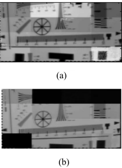
Raw images captured by Sensor A 1.8 V are reported in Fig. 7, before and after irradiations. The 16 different pixel-type regions can be easily recognized. Their organization is the one reported in Fig. 2. From the comparison of the two images, it can be seen that after irradiation, the standard 3T PHD (bottom left) as well as the partially pinned PHDs (top right)
Fig. 7. Raw images captured (a) before and (b) after 1 MGy(SiO2) with comparable illumination conditions for Sensor A 1.8 V. The integration time is
∼1 ms, and the gate voltage is set to 1 V. The 16-pixel variants are organized,
as illustrated in Fig. 2.
Fig. 8. Dark current evolution with TID for Sensor A 1.8-V pixels P1, P6, P13, and P14 of Table II. The dark current values in P2 and P13 are obtained for depleted gate (gate voltage> 0 V).
are not functional anymore, whereas all the gate overlap-based designs are able to provide an image. In order to study the radiation hardness of different PHD doping profiles proposed by the foundry and to compare with the optimized RHBD gate overlap solutions, the dark current evolution with TID is presented in Fig. 8. The results show that as expected, the 3T-standard PHD exhibits the higher absolute dark current value after a TID of 10 kGy(SiO2). (The dark current before
irradiation is comparable to the other 3T pixels.) This dark current increase at this TID level is mostly due to the TID-induced trapped charges and interface states in the Si/SiO2
interfaces (PMD and STI) which strongly contribute to the dark signal increase [22].
The 3T-standard partially pinned PHD has the lowest dark current before irradiation among all the studied technologies,
Fig. 9. Dark current as a function of gate voltage at a TID of 100 kGy for pixels with different overlaps between the gate and the PHD.
thanks to the p+ surface protection. However, at 10 kGy(SiO2), the dark current of this pixel type increases up
to ∼1 pA. As shown in Fig. 8, the absolute dark current value is lower in the partially pinned PHD than in 3T-standard PHD. It is possible that at this dose level, the induced positive trapped charges in the PMD reduce the effective doping of the p+ layer, thus allowing the PHD to be in contact with the oxide, in which defects contribute to the dark current increase. Above 10 kGy(SiO2), both partially pinned PHD
and standard PHD are not functional anymore. As regards the RHBD gate overlap solutions, it can be noted that they give the best performance in terms of dark current increase with TID even if some differences are highlighted between different variants.
Four different variants are reported in Fig. 8: the gate over-lap PHD (P2 or P6 shown in Table II) with an overover-lap distance of 0.3μm, the gate aligned PHD (P3 shown in Table II) with
d = 0 μm, the gate overlap and STI isolation (P5 shown
in Table II), and the PHD P13 having an n+ drain ring surrounding the PHD. One can see that the gate aligned PHD has the highest dark current compared to the gate overlap design at the optimum gate voltage.
Fig. 9 displays the dark current as a function of the applied gate voltage for pixels P2–P4. These pixels differ from each other for the overlap distance. It can be noted that for negative gate voltage, the dark current in the gate aligned design (d= 0) is lower than in the gate overlap designs. Furthermore, the increase of the overlap distance from 0.3 to 0.6μm leads to an augmentation of the dark current in this negative gate voltage region. This difference in dark current is most likely due to an enhanced gate-induced drain leakage [23] when the overlap is too large. For positive gate voltages, the best dark current is exhibited by gate overlap PHDs, whereas gate aligned PHD has higher dark current. In this case, as illustrated in Fig. 10(a), the induced defects in the spacer contribute to the dark current in the gate aligned design. Indeed, the spacer is in contact with the depleted region in this particular case. On the other hand, in the gate overlap designs, the spacer is no more in contact with the depleted region [see Fig. 10(b)], thus leading to a lower dark current in these pixels. As last remarks, it is possible to see that in terms of dark current performances, both gate overlap pixels have the same behavior for positive gate voltages (i.e., the optimum voltage for this pixel type).
Fig. 10. Illustrations of the dark current enhancement mechanism between (a) gate aligned PHD and (b) gate overlap PHD when the gate channel is depleted (positive gate bias). The depleted region is in contact with the spacers in the gate aligned design, thus leading to an increase of the number of defects contributing to the dark current.
Fig. 11. Dark current as a function of gate voltage at a TID of (a) 10 kGy and (b) 1 MGy for P2 and P13. The same behavior has been measured on the other CIS architectures and foundries. Illustrations of the dark current draining mechanism in (c) and (e) gate overlap and (d) and (f) n+drain PHDs.
The comparison between P5 and P6 highlights that there is no influence of STI used to improve the intrapixel isolation in the dark current. As it can be seen from Fig. 7, there is no evidence of short circuit between adjacent PHDs even in the region of high contrast. Thus, in this particular technology, STI isolation between diodes can be removed without any obvious drawback.
From Fig. 8, it can be seen also that two regimes can be found depending on the investigated TID range from the com-parison between gate overlap (pixel P2 shown in Table II) and gate overlap with n+ drain (pixel P13 shown in Table II). For
Fig. 12. Saturation voltage as a function of gate voltage at a TID of 1 MGy for different n+ drain pixel variants.
TID< 100 kGy(SiO2), the dark current reduction is enhanced
in the n+ drain design, whereas beyond 100 kGy(SiO2),
the two pixels exhibit mostly the same dark current level. In order to explain this difference, Fig. 11 reports the dark current measurements as a function of gate voltage at two different doses. At 10 kGy(SiO2), as shown in Fig. 11(a),
the gate overlap design exhibits the same dark current than the n+ drain design up to a gate voltage of 1.3 V. (The n+ drain design is slightly lower for all the examined gate voltage ranges.) In this gate voltage range, the gate channel is depleted and the PHD depletion region extends toward the STI sidewall. However, there is no dark current increase up to 1.3 V in the gate overlap PHD. As suggested in [6], in the considered gate voltage range, the STI sidewall p+ passivation may be sufficient to prevent the depletion region from reaching it.
At a gate voltage higher than 1.3 V, an increase of the dark current is observed in the gate overlap design up to values that are comparable to the partially pinned design, whereas the dark current continues to decrease in the n+drain design. This difference is due to the dark charges driving mechanism toward the n+ drain (biased at VDD) which is activated in the n+drain design. For gate voltages higher than 1.3 V, the depletion region reaches the STI sidewall in the gate overlap pixel, and the TID-induced defects in the STI contribute to the dark current increase. Conversely, as depicted in Fig. 11(d), in the other design, the dark charges coming from the STI sidewall are collected by the n+ drain, thus leading to a continuous reduction of the dark current with the increase of the gate voltage. For TID> 10 kGy(SiO2), the STI
radiation-induced positive trapped charge is sufficient to create an inversion channel all along the STI interface, thus turning on the dark current draining mechanism in the gate overlap design [see Fig. 11(e)]. In this case, the dark current decreases with increasing gate voltage in both investigated designs.
The reported dark current analysis has shown that adding the n+ drain activates the dark charges draining mechanism which occurs also in the gate overlap design after a certain TID. This suggests, indeed, that this proposed RHBD solution is promising since it allows controlling the drain of the dark charges at different TIDs. In order to evaluate the influence of the n+ drain design on the PHD optoelectrical performances, a preliminary analysis on the saturation behavior of the diverse pixel variants is performed.
Fig. 12 reports the saturation voltage as a function of the gate voltage for pixels without drain and for various n+drain dimensions investigated in this paper after 1 MGy(SiO2) of
irradiation. It can be seen that the saturation voltage is constant with the gate voltage for negative voltages.
For positive voltages, the saturation voltage decreases after a threshold value. It can be pointed out that the gate voltage value after which the saturation voltage starts to decrease depends on the pixel design. Indeed, in PHDs having the n+ ring, the saturation voltage decreases after 0.5 V, whereas for the other, the threshold voltage is between 1.1 and 1.5 V.
In the case of gate overlap without n+ drain, the saturation voltage decreases after 1.6 V. This result shows that the n+ drain design is an important parameter to take into account for the implementation of this RHBD solution in radiation-hard cameras. A bad design choice could lead to a strong reduction of the saturation voltage at a gate voltage too low to obtain an efficient dark current reduction through the draining mechanism.
VI. CONCLUSION
In this paper, a radiation hardness comparison of CIS tech-nologies at high TID levels is performed with the aim to eval-uate the vulnerability of the partially pinned PHD technology, to compare the radiation hardness of different manufacturing processes and to confirm the response of various standard and RHBD pixel types.
It has been pointed out that even if the 3T-standard partially pinned PHD has the lowest dark current before irradiation among all the studied technologies, and even if this technology is often considered as radiation tolerant in the community, at 10 kGy(SiO2), the dark current of this pixel type increases
up to ∼1 pA (comparable to the dark current of standard 3T PHDs at the same TID). This dark current increase has been mostly attributed to the induced trapped charges in the PMD which reduce the effective doping of the p+ layer, thus allowing the pinned PHD to be in contact with the defects in the Si/SiO2 interfaces contributing to the dark
current increase. Moreover, it has been shown that above 10 kGy(SiO2), the partially pinned pinned PHD functionality
is lost.
The comparison between the CIS postirradiation perfor-mances of several technologies has highlighted that the man-ufacturing process impacts the two main radiation-induced degradations: the threshold voltage shift of the pixel and the output stages of the readout chain and the dark current increase. It has been confirmed that 1.8-V MOSFETs exhibit the lower threshold voltage shift for all the tested technologies and that in both 3.3- and 1.8-V transistors, the nMOSFETs are the most radiation tolerant devices among both 1.8- and 3.3-V transistors. Regarding the dark current increase in various tested technologies, the results demonstrate that 1.8-V sensors exhibit the best performances by up to a factor of 7 for foundry C. Finally, it has been pointed out that although the main conclusions listed above are the same for all the tested technologies, the manufacturing process has an important impact on the absolute radiation hardness. Indeed, foundry
B exhibits the most radiation resistant MOSFETs, but CISs dark current increase is the largest in both 3.3- and 1.8-V architectures. Furthermore, these sensors suffer from radiation-induced nonuniformity, leading to a decrease of cameras’ performances. TID effects on foundry A 3.3-V architecture lead to a reduction of the overall sensor performances reduc-ing the linear useful range, in which the CIS can correctly operate. Conversely, 1.8-V architecture has shown the best performances after 1-MGy(SiO2) TID.
Finally, the comparison between various RHBD pixel vari-ants has highlighted that the gate overlap design still gives the best performance in terms of dark current for positive voltages applied to the gate, even on different CMOSs process than the one explored before [6]. On the other hand, this overlap has to be optimized in order to reduce nonuniformity linked to the pixel-to-pixel connection. The study of a new RHBD solution consisting in adding an n+ drain biased at VDD in the pixel has confirmed the charge draining mechanisms proposed in [6] and analyzed through the TCAD simulation in [7]. Furthermore, the study of this pixel variant has revealed that the dark charges draining mechanisms can be enabled at TID < 10 kGy(SiO2), thus leading to an improved control
of the dark current reduction in this range. It has, however, been shown that the dimensions of n+ drain are important since the activation of the charge drain mechanism affects the performances of the camera via the reduction of the saturation voltage.
Thanks to these results, it has been possible to clarify the role of the manufacturing process which is shown to be a key parameter to take into account when dealing with radiation resistant CIS development. The feasibility of the development of a full-size sensor with promising performances at high TID is confirmed. The next step will be to explore the proposed improvements, to integrate more functions on-chip in order to develop the full-size and fully integrated camera which could withstand the harsh environments aimed by the CAMRAD Project.
REFERENCES
[1] E. R. Fossum, “CMOS active pixel image sensors,” Nucl. Instrum.
Methods Phys. Res. A, Accel. Spectrom. Detect. Assoc. Equip., vol. 395,
no. 3, pp. 291–297, 1997.
[2] G. R. Hopkinson, “Radiation effects in a CMOS active pixel sensor,”
IEEE Trans. Nucl. Sci., vol. 47, no. 6, pp. 2480–2484, Dec. 2000.
[3] J. Bogaerts, B. Dierickx, G. Meynants, and D. Uwaerts, “Total dose and displacement damage effects in a radiation-hardened CMOS APS,”
IEEE Trans. Electron Devices, vol. 50, no. 1, pp. 84–90, Jan. 2003.
[4] High Radiation Tolerant B/W Camera. [Online]. Available: http://ddaqua.gobizkorea.com/catalog/product_view.jsp?blogId=huhu3& pageNo=1&pageVol12&listStyle=L&objId=668654
[5] High Radiation Tolerant Color Camera. [Online]. Available: http://ddaqua.gobizkorea.com/catalog/product_view.jsp?blogId=huhu3& pageNo=1&pageVol12&listStyle=L&objId=668653
[6] V. Goiffon et al., “Total ionizing dose effects on a radiation-hardened CMOS image sensor demonstrator for ITER remote handling,” IEEE
Trans. Nucl. Sci., vol. 65, no. 1, pp. 101–110, Jan. 2018.
[7] O. Marcelot, V. Goiffon, S. Rizzolo, F. Pace, and P. Magnan, “Dark current sharing and cancellation mechanisms in CMOS image sensors analyzed by TCAD simulations,” IEEE Trans. Electron Devices, vol. 64, no. 12, pp. 4985–4991, Dec. 2017.
[8] B. Pain et al., “Hardening CMOS imagers: Radhard-by-design or radhard-by-foundry,” Proc. SPIE, vol. 5167, Jan. 2004, pp. 101–110. [9] B. R. Hancock et al., “Multi-megarad (Si) radiation-tolerant integrated
[10] V. Goiffon, P. Cervantes, C. Virmontois, F. Corbiere, P. Magnan, and M. Estribeau, “Generic radiation hardened photodiode layouts for deep submicron CMOS image sensor processes,” IEEE Trans. Nucl. Sci., vol. 58, no. 6, pp. 3076–3084, Dec. 2011.
[11] E. R. Fossum and D. B. Hondongwa, “A review of the pinned photodiode for CCD and CMOS image sensors,” IEEE J. Electron Devices Soc., vol. 2, no. 3, pp. 33–43, May 2014.
[12] T.-H. Lee, R. M. Guidash, and P. P. Lee, “Partially pinned photodi-ode for solid state image sensors,” U.S. Patent 09 164 968, Nov. 5, 1999.
[13] P. R. Rao, X. Wang, and A. J. P. Theuwissen, “Degradation of CMOS image sensors in deep-submicron technology due to γ -irradiation,”
Solid-State Electron., vol. 52, no. 9, pp. 1407–1413, Sep. 2008.
[14] J. Tan, B. Buttgen, and A. J. P. Theuwissen, “Analyzing the radi-ation degradradi-ation of 4-transistor deep submicron technology CMOS image sensors,” IEEE Sensors J., vol. 12, no. 6, pp. 2278–2286, Jun. 2012.
[15] V. Goiffon, M. Estribeau, P. Cervantes, R. Molina, M. Gaillardin, and P. Magnan, “Influence of transfer gate design and bias on the radiation hardness of pinned photodiode CMOS image sensors,” IEEE Trans.
Nucl. Sci., vol. 61, no. 6, pp. 3290–3300, Dec. 2014.
[16] G. Anelli et al., “Radiation tolerant VLSI circuits in standard deep submicron CMOS technologies for the LHC experiments: Practical design aspects,” IEEE Trans. Nucl. Sci., vol. 46, no. 6, pp. 1690–1696, Dec. 1999.
[17] F. Faccio and G. Cervelli, “Radiation-induced edge effects in deep submicron CMOS transistors,” IEEE Trans. Nucl. Sci., vol. 52, no. 6, pp. 2413–2420, Dec. 2005.
[18] S. Rizzolo et al., “Multi-MGy total ionizing dose induced MOSFET vari-ability effects on radiation hardened CMOS image sensor performances,” in Proc. 17th Eur. Conf. Radiat. Effects Compon. Syst. (RADECS), Geneva, Switzerland, Jan. 2017.
[19] G. R. Hopkinson, A. Mohammadzadeh, and R. Harboe-Sorensen, “Radi-ation effects on a radi“Radi-ation-tolerant CMOS active pixel sensor,” IEEE
Trans. Nucl. Sci., vol. 51, no. 5, pp. 2753–2762, Oct. 2004.
[20] B. Dryer et al., “Gamma radiation damage study of 0.18μm process CMOS image sensors,” Proc. SPIE, vol. 7742, p. 77420E, Jul. 2010, doi:10.1117/12.863948.
[21] M. E. Cherniak, A. A. Smolin, A. V. Ulanova, and A. Y. Nikiforov, “Investigation of nonuniform degradation of CMOS-sensor light-sensitive surface under gamma-irradiation,” in Proc. 15th Eur. Conf.
Radiat. Effects Compon. Syst. (RADECS), Sep. 2015, pp. 1–3, doi: 10.1109/RADECS.2015.7365623.
[22] V. Goiffon, C. Virmontois, P. Magnan, S. Girard, and P. Paillet, “Analysis of total dose-induced dark current in CMOS image sensors from interface state and trapped charge density measurements,” IEEE Trans.
Nucl. Sci., vol. 57, no. 6, pp. 3087–3094, Dec. 2010.
[23] T. Y. Chan, J. Chen, P. K. Ko, and C. Hu, “The impact of gate-induced drain leakage current on MOSFETs scaling,” in IEDM Tech.