O
pen
A
rchive
T
OULOUSE
A
rchive
O
uverte (
OATAO
)
OATAO is an open access repository that collects the work of Toulouse researchers and
makes it freely available over the web where possible.
This is an author-deposited version published in:
http://oatao.univ-toulouse.fr/
Eprints ID : 14526
To link to this article : DOI :
10.1109/TNS.2014.2369436
URL :
http://dx.doi.org/10.1109/TNS.2014.2369436
To cite this version :
Virmontois, Cedric and Toulemont, Arthur and
Rolland, Guy and Materne, Alex and Lalucaa, Valerian and Goiffon,
Vincent and Codreanu, Catalin and Durnez, Clementine and
Bardoux, Alain
Radiation-Induced Dose and Single Event Effects in
Digital CMOS Image Sensors
. (2014)
IEEE Transactions on Nuclear Science, 61 (6). pp. 3331-3340. ISSN
0018-9499
Any correspondance concerning this service should be sent to the repository
administrator:
[email protected]
Abstract— This paper focuses on radiation-induced dose and
single event effects in digital CMOS image sensors using pinned photodiodes. Proton irradiations were used to study cumulative effects. As previously observed, the dark current is the main electrical parameter affected by protons. The mean dark current increase appears proportional to Srour’s universal damage factor. Therefore, the degradation is mainly attributed to displacement damage in the pinned photodiode. Heavy ion tests are also reported in this work. This study focuses on single event effects in digital CMOS imagers using numerous electronic functions such as column ADCs, a state machine and registers. Single event transients, upsets and latchups are observed and analyzed. The cross sections of these single events are transposed to specific space imaging missions in order to show that the digital functions can fit the mission requirements despite these perturbations.
Index Terms— Pinned Photodiode (PPD), Active Pixel Sensor
(APS), Monolithic Active Pixel Sensor (MAPS), CMOS Image
Sensor (CIS), Displacement Damage (Dd) dose, Total Ionizing
Dose (TID), Random Telegraph Signal (RTS), Single Event Effects (SET)
I. INTRODUCTION
PACE imaging missions require high performance image sensors. Thanks to their good electro-optical performance, low power consumption and tolerance to the space radiation environment, CMOS image sensors [1] are preferred over Charge Coupled Devices (CCD) in many future space missions. However, CMOS image sensors are generally planned to be used as pure analog devices, in the same way as CCD [2], [3], which means the possibilities offered by CMOS technology will not be fully exploited. Indeed, with CMOS imagers, several electronic functions such as column ADCs, machine state and registers can be integrated on the chips and the ASIC video chain previously used for analog imagers can be removed in order to improve the focal plane of the imaging payload [4]. With these advantages, it would seem very worthwhile to focus on digital CMOS image sensors integrating numerous electrical functions surrounding the pixel array in order to take full advantage of the CMOS technology. However, CMOS imagers are known to be sensitive to dose effects [5]-[7], especially when using pinned
This work was supported in part by the CNES R&T Parts and CNES OTOS Program.
C. Virmontois, A. Toulemont, G. Rolland, A. Materne, C. Codreanu, C. Durnez and A. Bardoux are with CNES, 31401 Toulouse, France. (Phone: +33 5 6128 2166, fax: +33 5 6127 8351; e-mail: [email protected]).
V. Lalucaa and V. Goiffon are with Université de Toulouse, ISAE, 31055 Toulouse, France.
photodiodes [8]-[10], and digital CMOS functions are sensitive to single event effects [11]. Smart imagers integrating electronic functions therefore need to be evaluated to determine their tolerance to both dose and single event effects. Numerous studies deal with ionizing and non-ionizing dose effects [5]-[10] while only a few discuss single events [12]-[15]. Earlier studies [12], [13] have focused on radiation-tolerant devices using hardening-by-design techniques. More recent ones [14], [15] are dedicated to single event effects in basic pixel array structures. However, no dedicated study evaluates these effects in last generation digital imagers integrating electronic functions such as column ADCs, microcontrollers and registers.
This study focuses on two digital CMOS imagers using pinned photodiode (PPD). The technology and the design differ from one imager to the other, but no hardening-by-design techniques were used for either imager. We first examine dose damage. The dark current increase, due to proton irradiation, is analyzed and compared to the universal damage factor [16] in order to emphasize the displacement damage contribution. Particular attention is given to dark current distributions where peaks related to dark current spectroscopy [17] appear, as previously observed in CMOS imagers [18]. Dark Current Random Telegraph Signal (DC-RTS) is also investigated and compared to previous results [19]. The second part of the paper focuses on single event effects. The imagers are biased and operated during heavy ion tests in order to analyze the effects of Single Event Transients (SET) and Single Event Upsets (SEU) on the images and Single Event Latchups (SEL) on the power supply. This part also addresses the difficulty of performing such SEE tests on these specific devices. The final part of the paper shows how these imagers can fit space imaging mission requirements for Low Earth Orbit (LEO) and Geostationary Earth Orbit (GEO) under various shielding conditions.
II. EXPERIMENTAL DETAILS
The studied components are CMOS image sensors from two different foundries, designed using different CIS processes and technology nodes as reported in Tab. I. Both devices contain integrated digital parts including column ADCs, a microcontroller and registers, as can be seen in Fig. 1. The CIS1 device presents two epitaxial layer thicknesses: the standard thickness of 5 µm, and a 12 µm thickness. This study examined both layer thicknesses. The CIS2 device has only one epitaxial thickness: less than 4 µm.
The CIS1 and CIS2 devices were exposed to protons at the Kernfysisch Versneller Instituut (KVI) facility.
Radiation-Induced Dose and Single Event
Effects in Digital CMOS Image Sensors
Cédric Virmontois, Member, IEEE, Arthur Toulemont, Guy Rolland, Alex Materne, Valerian Lalucaa, Vincent
Goiffon, Member, IEEE, Catalin Codreanu, Clémentine Durnez and Alain Bardoux
S
HI S doc um ent is a tem plat e for Mi cro soft WoTABLEI DEVICE CHARACTERISTICS
Imagers CIS1 CIS2
Technology node 180 nm 90 nm Pixel architecture 8T PPD 4T PPD Pixel Pitch (µm) 5.5 1.4 Epitaxial thickness (µm) 5 & 12 < 4 Array 2048 × 2048 2592 × 1944 Irradiation Proton / Heavy ion 50 and 150 MeV γ-rays / Heavy ion 60 MeV Proton /
TABLEII IRRADIATION CHARACTERISTICS
Irradiation type Imagers Fluence (cmDose rate -2) / (TeV/g) DDD (krad TID (SiO2))
50 MeV proton CIS1 1.4 × 10¹⁰
54 2 50 MeV proton CIS1 5 × 10¹⁰ 194 8 50 MeV proton CIS1 1.3 × 10¹¹
504 20.5 50 MeV proton CIS1 2 × 10¹¹
776 31.5 150 MeV proton CIS1 3 × 10¹¹
645 21 60 MeV proton CIS2 1 × 10¹¹
335 13.8 γ-rays CIS2 310 rad/h / 4.5 γ-rays CIS2 310 rad/h / 9
TABLEIII HEAVY ION CHARACTERISTICS
Ions Energie (MeV) (p.cmMax Flux -2.s-1) (MeV.mgLET -1.cm-2) (µm Si) Range
UCLHIGH LET COCKTAIL (M/Q=5)
124Xe25+ 420 1,5.104 67,7 37 84Kr17+ 305 1,5.104 40,4 39 40Ar8+ 151 1,5.104 15,9 40 20Ne4+ 78 1,5.104 6,4 45
15N3+ 60 1,5.104 3,3 59
UCLHIGH RANGE COCKTAIL (M/Q=3.3)
83Kr25+ 756 1,5.104 32,6 92 58Ni18+ 567 1,5.104 20,4 100 40Ar12+ 372 1,5.104 10,2 117
22Ne7+ 235 1,5.104 3 216
13C4+ 131 1,5.104 1,1 292
As shown in Tab. II, the energy ranges from 50 to 150 MeV. The total displacement damage dose ranged from 54 to 776 TeV/g and the TID ranged from 2 krad(SiO2) to 30
krad(SiO2). The Devices were unbiased and placed in
antistatic foam during the tests. Proton irradiation tests were performed at room temperature. The post-irradiation characterization campaign was performed three weeks after proton irradiation tests and the devices were stored at room temperature. Two CIS2 devices were irradiated with γ-rays using 60Co source at the Université Catholique de Louvain
(UCL, Belgium). The dose rate was 310 rad(SiO2) per hour
and the devices were biased for 20% of the irradiation time. The cumulative dose reached 4.5 krad(SiO2) for one device
and 9 krad(SiO2) for the second. γ-rays irradiation tests were
performed at room temperature. The post-irradiation characterization campaign was performed the day after the γ-rays tests.
Fig. 1. Schematic diagram of the CIS 1 and CIS 2 imagers.
All devices were placed in a temperature-controlled chamber during dark current and RTS measurements. The RTS detection algorithm, based on the edge front method, is described in [19]. All other electro-optical measurements were performed at ambient temperature.
Heavy ion tests were performed at UCL using the two available cocktails described in Tab. III. “High LET” and “High Range” cocktails were used to maximize the range of ion penetration and the range of Linear Energy Transfer (LET) investigated. During heavy ion irradiation, the sensors were operated using a proximity board in the vacuum chamber. The biasing was applied using a power supply that can control and limit the current. The SEL detection threshold was set at 1.5 times the nominal value, and the current limit was fixed at twice the nominal value. This limit was increased for specific tests in order to observe whether or not the SELs were destructive. Another computer was used to operate the device. Two main software applications were developed. The first was used to collect frames during irradiation, with the integration time set to 1 ms, similar to high resolution imaging missions. The second application was used to program registers to low or high states; it read the register’s state every 200 ms, counting any change and re-writing the nominal values. This software made it possible to analyze the SETs and SEUs. The heavy ion flux was adapted for each run in order to obtain a precise SEE cross section (i.e. when the cross section increases, the flux is reduced and vice-versa). The maximum fluence reached 2.107 cm-2.
One important aspect of heavy ion tests concerns the layer above the silicon. As heavy ion ranges are limited, any cover glass or metal shielding must be removed. Moreover, passivation layers and metallic lines above the silicon epitaxial layer have to be estimated in order to select constant LETs when ions pass through the epitaxial layer of silicon. Indeed, the LET is not constant along the track in the silicon, and the Bragg peak appears when the particle reaches the maximum of its range [14]. Equivalent Silicon thickness can be deduced for each of the CIS’s top layers. Equivalent silicon thickness is the
Fig. 2. Mean dark current variation with the transfer gate bias during integration. The minimum dark current for CIS2 shows a negative bias whereas the minimum dark current for CIS1 never goes below 0V. The measurement temperature is 22°C.
product of the density ratio between the silicon and the other material times the thickness of the other materials (for example 1 µm of copper is equivalent to 3.85 µm of silicon). These materials can be silicon oxide, silicon nitride, copper, aluminum, and even polymer in the case of sensors equipped with microlenses. The top layers for both CIS1 and CIS2 have equivalent silicon thicknesses, close to 5 µm, so the LET of each ion is constant in the different epitaxial layers [14], with the exception of Xenon in the “High LET” cocktail. However, the Xenon LET stays above 60 MeV.cm².mg-1 for the epitaxial
layers of both devices, even the 12 µm one.
The recorded SEL and SEU cross sections were then processed using the OMERE [20] calculation software in order to estimate the occurrence rate for specific ten-year imaging missions in Low Earth Orbit (LEO) and Geostationary Earth Orbit (GEO).
III. CUMULATIVE DOSE EFFECTS
Dose effects can be broken down into two categories: ionizing effects and non-ionizing effects. Each effect is known to increase dark current in CIS using PPDs [8]-[10] and to induce DC-RTS. Moreover, changes in pinning voltage, Photon Transfer Curve (PTC), and especially Full Well Capacity (FWC), have been reported recently [10]. This is why this section presents proton induced ionizing and non-ionizing dose results. One part focuses on dark current and RTS, and a final part discusses damage to other electro-optic parameters.
A. Mean dark current
Before presenting the radiation-induced dark current results, it is important to point out the effect of the Transfer Gate (TG) bias on dark current. Negative bias is commonly applied to the imager transfer gate during integration, which is the case for many CIS imagers using PPDs and the CIS2 imager studied here. This bias puts the TG channel in accumulation mode [21] and implies recessing of the space charge region from the TG and the surrounding Shallow Trench Isolation (STI)
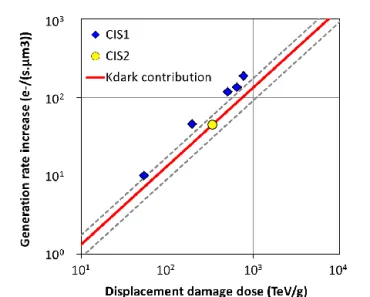
Fig. 3. Mean dark current increase after proton tests. Results are compared with UDF [16] showing the displacement damage effects. TID effects seem negligible on CIS 2 whereas they are significant on CIS1. Measurement temperature is 22°C. The Kdark is adapted to this temperature.
regions [10]. The result is that dark current is reduced, as can be seen in Fig. 2 (yellow curve on the left-hand side). Negative bias is used for all CIS2 results in the paper. CIS1 uses a specific TG (probably high VT transistor), and it
behaves differently. Fig. 2 shows the minimum dark current for VLOWTG equal to 0 V. Therefore, the CIS1 TG seems to be
accumulated at 0 V. This voltage is applied to CIS1 for all results presented herein.
The mean dark current measured three weeks after proton irradiations is shown in Fig. 3. The generation rate increase is plotted against the displacement damage dose (DDD).This rate corresponds to the dark current increase divided by the depleted volume (the depleted volume is estimated using TCAD simulation with the doping profile of the implants). The Universal Damage Factor (UDF) [16] is plotted to observe dark current due to displacement damage only. While CIS2 is consistent with UDF, the results obtained on CIS1 are slightly above the red line, which means that even if displacement damage induces the main increase, Total Ionizing Dose (TID) has a significant effect on CIS1 [10]. This discrepancy could be attributed to the transfer gate bias during integration. As TID generates defects in silicon oxide and at the Si/SiO2 interfaces, the recessing of the space charge
region from these areas induces better tolerance to TID. Negative bias is not applied to the CIS1transfer gate during integration for improved anti-blooming performances. Thus, the space charge region can touch the STI, which brings about a TID-induced dark current increase. Another possible hypothesis is based on the distance between the space charge region and the surrounding STI regions. Indeed, if this distance is not correctly adapted, the interface can generate TID-induced dark current.
B. Dark current distribution
The mean dark current results and dark current distributions complement one another. As can be seen in Fig. 4 and 5, the dark current distribution for CIS1 provides additional information. As the figure shows, the dark current spikes increase with the displacement damage dose, and the
Fig. 4. Dark current distribution for CIS1 before and after proton tests (low doses). The dark current spikes increase with displacement damage dose. Ionizing effects cause a shift in the maximum values in the post-irradiated distributions.
Fig. 5. Dark current distribution for CIS1 before and after proton tests (high doses). The dark current spikes increase with displacement damage dose. Ionizing effects cause a shift in the maximum values in the post-irradiated distributions.
maximum values in the distribution shift to higher values as a results of TID effects [22]. The proton results for CIS1 are presented in two figures, illustrating what happens at low doses (Fig. 4) and at high doses (Fig. 5). Both figures show significant hot pixel skew, which is proportional to displacement damage. There is also a slight shift in the entire distribution, which is specific to TID and consistent with the results of Fig. 3.
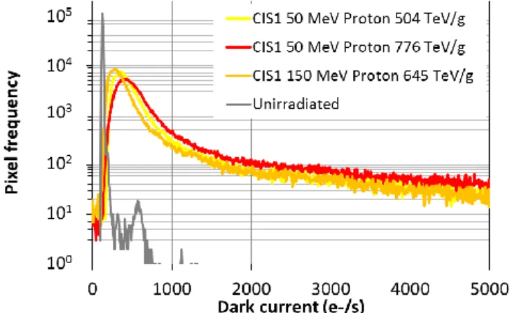
A specific behavior is observed in Fig. 4, in which a peak appears inside the pixel skew. The peak is previously reported in [18] and has been attributed to dark current spectroscopy [17] phenomenon. Indeed, dark current in CIS1 is low enough to observe this spectroscopy of defects generation rate. This peak can also be seen in Fig. 6, which shows the proton results for CIS2. At a higher dose, the peak is drowned due to the large amount of defects with different generation rates. However, this technique needs to be investigated in last generation CIS to bring new insight concerning defects and displacement damage physics. Fig. 6 presents the variation in the peak with temperature. The activation energy of the dark current peak [18] is estimated to be around 0.82 eV. This result suggests that this peak corresponds to a specific defect; V2(-/0) which is proposed in [18] and consistent with the
results presented in this study.
Fig. 6. Dark current distributions for CIS2 before and after irradiation with 60 MeV protons. The displacement damage dose is 335 TeV.g-1, and the TID
peaks at 13 krad (SiO2). The measurements were taken at 25 and 35°C.
Fig. 7. Dark current distributions for CIS2 before and after irradiation with γ-rays. The measurements were taken at 25°C.
Fig. 7 highlights the TID tolerance of CIS2. The dark current histogram remains almost unchanged, even after 9 krad(SiO2).
These results are consistent with the results presented in Fig. 3. A detailed study on γ-ray-induced dark current on CIS1 has been completed, however the results are not presented here. Interesting modeling results are presented in Fig. 8 where the distribution is normalized by the number of pixels, the PPD’s depleted volume and the displacement damage dose. The tail of the dark current histogram behaves exponentially. The exponential law used to fit the data is:
f(x)kexp(x) (1)
where 1/λ is the mean value of the distribution and k is a constant. The mean values obtained in a previous study [18] are compared with the experimental data. The blue curve corresponds to 6 ke-/s, which was used to fit previous CIS data
using 3T pixels with conventional photodiodes [18], [22]. The green curve corresponds to the average value, 1.8 ke-/s (There
is an error on this value in [18], the paper states a value of 18 ke-/s, but the correct value is 1.8 ke-/s) and fits the data
obtained on 4T pixels using PPDs in [18]. The decrease in average values can be explained by the use of very small PPDs in [18], where the border effects become significant [23]. The results in Fig. 8 show that the average value obtained using 3T pixels fits with the CIS1 data, even though CIS1 using PPD
Fig. 8. Normalized dark current increase distribution of CIS1. The distributions are normalized by the depleted volume of the PPD (extracted using TCAD simulation), the number of pixels and the displacement damage dose. The exponential laws are plotted in blue and green lines, the average value of the laws are 6 ke-/s for the blue curve, which fits the experimental
CIS1 data, and 1.8 ke-/s for the green curve, which fits the previous PPD CIS
data [18].
with 4T pixels. Therefore, CIS1 seems not to suffer from border effects. From these sets of data and previous studies [18], [24], it can be concluded that the exponential fit method using 6 ke-/s works with 3T and 4T pixels, using conventional
and pinned photodiodes. However, this average value can be reduced in the case of small pixels, where border effects can appear. Further analysis of this modeling technique should be done, especially using small PPD pixels.
C. Dark current Random Telegraph Signal
The dark current RTS was examined on the imagers. The main RTS parameters are presented, the number of levels, the maximum amplitude distribution and the mean time between transitions. Previous studies [25]-[27] provide specific values, such as the average maximum amplitude, the concentration of defects per dose, and the time constant between transitions.
Fig. 9 shows the number of levels per RTS pixel. A large number of levels are found after proton irradiations, even for the lowest doses. As explained in [25], this means that the observed RTS is related to displacement damage RTS, i.e. metastable defects created by displacement damage can present multi-level RTS. This is not the case for TID-induced DC-RTS [25]: as can be seen in the figure, the maximum number of levels after γ-ray irradiations is 3. Moreover, the behavior of the proton curve is the same for both devices, whereas the γ-ray curves decrease more sharply. These results are consistent with [25].
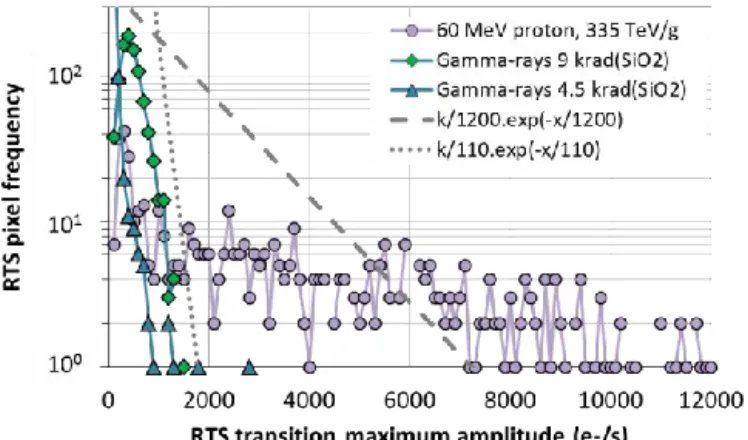
Fig. 10 shows the maximum amplitude between transitions for CIS1 after proton irradiation. As previously reported [25]-[27], the distributions behave exponentially. The exponential law is defined as:
f(x)kexp(x) (2) where 1/λ is the mean value of the distribution and corresponds to the specific signature of the DC-RTS type [25].
k’ is related to the number of pixels in the array and to the
Fig. 9. Distributions of the RTS number of levels for CIS1 and CIS2. The highest number of levels is observed after proton irradiation.
Fig. 10. RTS transition maximum amplitude distributions. The exponential law using an average value of 1200 e-/s is plotted, and is consistent with the
CIS1 data. All measurements were taken at 23°C.
Fig. 11. RTS transition maximum amplitude distributions. The exponential law using an average value of 1200 e-/s and 110 e-/s is plotted here and is
consistent with the CIS2 data. All measurements were taken at 23°C.
concentration of RTS centers. This k’ parameter could be expressed as:
kCdef bNpixVdep (3) where Cdef is the number of detected RTS defects (per
volume), b is the bin size of the histogram, Npix is the number
of pixels in the studied array, and Vdep is the depleted volume
Fig. 12. Distribution of mean times between RTS transitions for CIS1. Similar time constants of 4 s can be extracted from all distributions.
Fig. 13. Distribution of mean times between RTS transitions for CIS 2. TID-DC-RTS clearly behaves differently than DDD TID-DC-RTS.
to displacement damage [25], the exponential law is plotted. The experimental data complies with this value, suggesting that the RTS observed is mainly due to displacement damage. Moreover, using Equation (3) the concentration of metastable defects is estimated to be 45 metastable defects/cm3/(MeV/g).
This value is slightly higher than that reported in [27]. This discrepancy can be explained by the exponential fit of the data.
Fig. 11 shows the same distribution for CIS2 after proton and γ-rays tests. There is clear evidence that the DC-RTS is different when due to TID than when due to DDD [25]. The γ-ray data were fitted using an average exponential value of 110 e-/s [25] whereas the proton data show a larger average value
closed to the DDD.
Fig. 12 and 13 provide information on the mean time between transitions. This parameter allows the time constant to be estimated when the curve behaves exponentially. Fig. 12 shows the results for CIS1. The behavior is similar to a previous study [25], and the extracted time constant from the data is 4 s. This value was reported in [25] for RTS due to displacement damage. The results obtained using this parameter suggest that the observed proton-induced DC-RTS is mainly due to displacement damage. Fig. 13 shows the difference between TID RTS and DDD RTS. A similar time constant can be extracted from proton data. The γ-ray data
Fig. 14. Picture of digital CIS showing the different parts where SEE can be detected.
behave differently, and it is not possible to extract a time constant.
D. Electro-optic and electronic parameters
The CIS1 devices were fully characterized after radiation tests. Electro-optic transfer function (linearity), noise, photon transfer curve, quantum efficiency and photon response non-uniformity were evaluated. The measurements performed on CIS1 reveal only a decrease of the FWC. This decrease is less than 5% after proton irradiation and can be attributed to leakage current under the TG [10]. No ADC degradation, no threshold voltage of the transistor variation, no microcontroller and register damage, neither charge to volt conversion factor change was reported within the tested dose range.
IV. SINGLE EVENT EFFECTS
The main challenge before using digital CMOS imagers with un-hardened design for space missions is single event evaluation. Indeed, it is important to know how the images are impacted by this phenomenon, and how high the occurrence rate is for these events. Fig. 14 shows the parts of the digital CIS in which SEE can occur. The pixel array is affected by SETs only, whereas ADCs, microcontrollers, and registers can suffer SEUs and SELs. This section is divided in three subsections, each of which addresses a specific single event. The last subsection covers the in orbit analysis using the SEE results obtained during heavy ion tests.
A. Single Event Transient
When a charged particle impinges the epitaxial silicon layer of the imagers, the amount of charge it creates can be collected in part by the photosensitive element in the pixels. These charges are collected by one or several pixels depending on their amount. Previous studies report SETs in 3T pixels using conventional photodiodes [14]. This work reports SETs in different pixel pitches and different design architectures. The authors also compared SETs collection using CIS with epitaxial layer or bulk silicon, arriving at several conclusions:
- For identical pixel design, pitch does not change the size of SET clusters. This mean that surface recombination is not a significant process.
- For identical pixel pitch and using high resistivity bulk CIS, design does not change the size of the SET clusters
- CIS using a high resistivity epitaxial layer on top of low resistivity bulk reduce the size of the cluster, and the number
Fig. 15. Experimental collected charge and simulation for CIS1 using 5 µm and 12 µm epitaxial layer thicknesses. The ratio of collected charge in both epitaxial layers is plotted as an inset.
of the collected charges compared to CIS using only high resistivity bulk silicon.
The Final perspective presented by the authors is a comparison of different epitaxial thicknesses. In a more recent study [15], the authors investigated SETs in PPD CIS with anti-blooming function, from different foundries. The study reveals that the anti-blooming function can reduce the size of the SET cluster.
In this section, the results obtained on CIS1 devices with two epitaxial thicknesses are presented. The two UCL cocktails are used to maximize the number of LETs investigated. Fig. 15 shows the collected charges following the LET, for both epitaxial thicknesses. The experimental data are not consistent with SRIM simulations. The discrepancy is due to the large amount of recombined charges in the highly doped substrate or in the surface containing the transistors, STI and surface oxides. The collected charges estimated with SRIM can be express as:
NSRIM NcolNSrecNBrec (4) where Ncol corresponds to the collected charge in the epitaxial
layer, NSrec is the surface recombined charges and NBrec
corresponds to the recombined charges in the bulk (substrate), because SRIM considers the collected charge in the epitaxial layer without taking into account the recombination process. The measurement data can be express as:
NMes Ncol NFun (5) where NFun corresponds to the additional charges collected in
the bulk area through the field-funneling effect [28], [29]. This effect is due to the modification of high-low junction between epitaxial layer and the bulk by the large amount of deposited charges. The phenomenon can be defined by the increase of the effective epitaxial layer thickness which induces an increase of the collected charges. However, SRIM results are higher than experimental data, therefore, the latter phenomenon is negligible compare to recombination process.
It is difficult to deduce where the maximum of the recombination process occurs, as substrate and surface
recombination are proportional to the size of the pixel cluster collected the charges. However, we can analyze and compare several ratios. First, using SRIM simulation, the ratio between the collected charges in 5µm and 12µm epitaxial layer is equal to the thickness ratio. The result is consistent as SRIM only take into account the deposit charges in the epitaxial layer without recombination process. The measurement data provide the ratio of the collected charges in 5µm and 12µm epitaxial layer, which is not equal to the epitaxial thickness ratio but to the ratio of the pixel cluster surface. This experimental result implies that collection mechanisms are mainly related to the surface. The length of the integration time was also investigated during the heavy ion tests. The results show a similar collected charge when the integration times vary from 0.5 ms to 100 ms suggesting that charge depositing and diffusion mechanisms are lower than this investigated duration.
B. Single Event Upset
Single event upsets occur in digital components; when a memory is fixed to a particular value, the amount of charge generated in the silicon by charged particles can change this nominal value. As explained in the experimental section, specific software was used to program the registers of CIS1 to a high state or low state. Then the value of each register was read every 200 ms. The software counts SEUs and re-writes the nominal value of the registers as soon as they change.
Fig. 16 shows the cross section of SEUs obtained by programming high states and low states. The results are close to each other indicating that registers are not more sensitive to SEUs when their states are high or low. While the cross section is significant at high LET, it has to be noted that not all registers trigger image corruption. More than 30 registers were tested, but only a few registers, such as gain or integration time registers, can actually corrupt the images.
C. Single Event Latchup
Particular attention was given to latchup events, which can be destructive. For space applications, especially star trackers, the CIS used are generally hardened to SEL [13]. CIS1 and CIS2 were irradiated under bias using a power supply that can control and limit the current to prevent a destructive overcharge. On the CIS2, no latchup was observed during tests
Fig. 16. SEU cross section following the ion LET. High state and low state cross section are closed. The Weibull function is plotted to fit the data and estimate LET threshold.
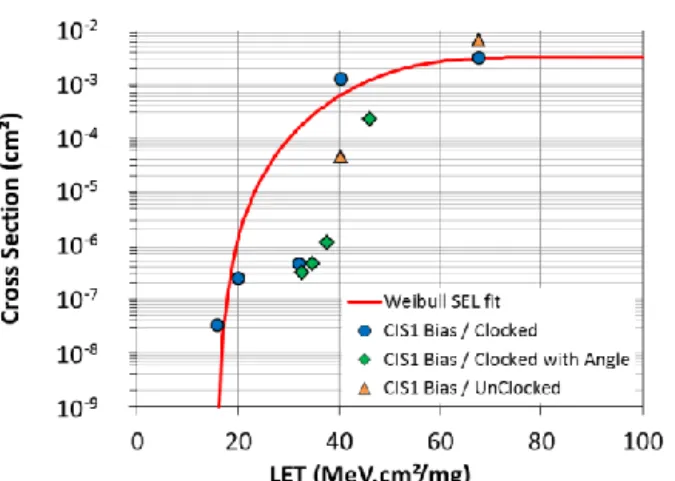
Fig. 17. SEL cross section following ion LET. Data from several irradiation tests are plotted here. The blue circles correspond to device bias (clocked) and the orange triangles correspond to device bias (un-clocked). The green diamonds correspond to device bias (clocked) but using an angle to vary the effective LET. The Weibull function is plotted here to estimate the LET threshold.
for fluence reaching 107 cm-2. These positive results are
thought to be due to the doping of the epitaxial layer and the deep-well implants available and used in this technology, which prevents latchups. CIS1 devices are made using another process and are not immune to SELs. As can be seen in Fig. 17, CIS1 was studied in different operating modes. First, the device was biased and operated in nominal mode to take pictures. The number of SELs increases with LET, and the values can be fitted using the Weibull function. Several devices were irradiated to obtain this curve and provide a precise LET threshold of around 16 MeV. The threshold is higher than the maximum LET the protons can produce as a result of ionizing and by non-ionizing effects in silicon. However, layers of specific metals, such as copper and tungsten, are used in CIS leading to higher LET if the protons interact with these metals by displacement damage.
The devices were also irradiated biased, but without operational signals, and the results are similar (as show in the figure), especially for Xenon ion. A greater discrepancy was observed for Krypton, but it was within the error bar. As the operating mode is difficult to implement for such radiation tests, the result proves that this particular devices does need to be in operating mode (i.e., clocked mode) for the tests to be performed on it. Additional results are presented by green diamonds. These last results are obtained using a tilt angle in order to increase the effective LET. These results are slightly below the nominal results suggesting that this is not a straight-forward method for devices using a silicon epitaxial layer.
D. Imaging mission in Low Earth Orbit (LEO) and Geostationary Earth Orbit (GEO)
The OMERE calculation software was used to estimate the single event occurrence rate for a specific mission. This paragraph focuses on the SEL rate, as this is the main issue for space applications.
Fig. 18 and 19 show the SEL rate per day with different shielding thicknesses. The thickness is provided in equivalent aluminum mm. The different curves represent the mean occurrence over the course of the 10 years, with or without taking into account the solar ions. The red squares correspond
to the worst days and the blue circles correspond to the worst 5 minutes. We note that these occurrences are not negligible, and that using an anti-latchup system is imperative when using this device for LEO or GEO missions. The last point concerns the difference between these orbits: the rate of occurrence will be higher in GEO than in LEO missions. Further analysis of this point is required.
V. CONCLUSION
Digital CMOS image sensors processed using different CIS technologies were evaluated for space radiation tolerance. Cumulative doses and single event effects induced degradation on these imagers. Dark current increase due to displacement damage and total ionizing dose were estimated. Mean dark current, dark current distribution and RTS were found to be mainly attributed to displacement damage. UDF and exponential modeling can predict the degradation observed in the investigated devices. We note that CIS1 does not suffer from border effects. Single event effects were analyzed. The SET study shows that the main collection process is related to the surface. The investigated integration times do not influence charge collection. SEUs are not sensitive to low or high register states here. SELs occur in CIS1, and the results show that SEL tests can be performed using devices under operating mode as well as devices biased without operating mode. Finally, for LEO or GEO space mission the main issue remains SELs and anti-latchup systems are imperative.
Fig. 18. SEL rate for a 10-year LEO mission.
ACKNOWLEDGMENT
The authors would like to thank the CNES expertise laboratory for their help, especially Helene Chauvin, Kateryna Kiryukhina and Guy Perez. They also wish to thank Mathieu Boutillier, CNES for their assistance during proton irradiations. Final thanks go to Melanie Raine for critical assessment of this study.
REFERENCES
[1] P. Lee, R. Gee, M. Guidash, T. Lee, and E. R. Fossum, “An active pixel sensor fabricated using CMOS/CCD process technology,” in Proc. IEEE Workshop on CCDs and Advanced Image Sensors, pp. 115–119, 1995. [2] R. Le Goff, P. Pranyies and I. Toubhans, “Focal plane AIT sequence:
evolution from HRG-SPOT5 to PLEIADES-HR”. in Proc 6th International Conf. on space Optics, Estec, Noordwijk, The Netherlands, Jun. 2006.
[3] J-L Lamard, C. Gaudin-Delerieu, D. Valentini, C. Renard, T Tournier, and J-M Laherrere, “Design of the high resolution optical instrument for the Pleaides HR earth observation satellites,” in Proc. ICSO, 2004. [4] K. Murthy, D. Robinson, M. Shearn, B. D. Smiley, A. H. Chau and J.
Levine, “SkySat-1: very high-resolution imagery from a small satellite,” Proc. SPIE Remote Sensing, Sept. 2014.
[5] G. R. Hopkinson, “Radiation effects in a CMOS active pixel sensor,” IEEE Trans. Nucl. Sci., vol. 47, no. 6, pp. 2480–2484, Dec. 2000. [6] E.-S. Eid, T. Y. Chan, E. R. Fossum, R. H. Tsai, R. Spagnuolo, J. Deily,
W. B. Byers, and J. C. Peden, “Design and characterization of ionizing radiation-tolerant CMOS APS image sensors up to 30 Mrd (Si) total dose,” IEEE Trans. Nucl. Sci., vol. 48, no. 6, pp. 1796–1806, Dec. 2001. [7] J. Bogaerts, B. Dierickx, G. Meynants, and D. Uwaerts, “Total dose and
displacement damage effects in a radiation-hardened CMOS APS,” Trans. Electron Devices, vol. 50, no. 1, pp. 84–90, 2003.
[8] M. Innocent, “A radiation tolerant 4t pixel for space applications,” in Proc. IISW, 2009
[9] P. R. Rao, X. Wang, and A. J. P. Theuwissen, “Degradation of CMOS image sensors in deep-submicron technology due to γ-irradiation,” Solid-State Electron., vol. 52, no. 9, pp. 1407–1413, Sep. 2008. [10] V. Goiffon, M. Estribeau, O. Marcelot, P. Cervantes, P. Magnan, M.
Gaillardin, C. Virmontois, P. Martin-Gonthier, R. Molina, F. Corbière, S. Girard, P. Paillet and C. Marcandella, “Radiation Effects in Pinned Photodiode CMOS Image Sensors: Pixel Performance Degradation Due to Total Ionizing Dose,” IEEE Trans. Nucl. Sci., vol. 59, no. 6, pp. 2878-2887, Dec. 2012.
[11] P.E. Dodd, M.R. Shaneyfelt, J.R. Schwank, and J. A. Felix, “Current and future challenges in radiation effects on CMOS electronics,” IEEE Trans. Nucl. Sci., vol. 57, no. 4, pp. 1747–1763, Aug. 2010.
[12] G. Hopkinson, A. Mohammadzadeh, and R. Harboe-Sorensen, “Radiation effects on a radiation-tolerant CMOS active pixel sensor,”IEEE Trans. Nucl. Sci., vol. 51, no. 5, pp. 2753–2762, 2004. [13] M. Beaumel, D. Hervé, D. Van Aken, P. Pourrouquet and M. Poizat,
“Proton, Electron and Heavy Ion Single Event Effects on the HAS2 CMOS Image Sensor” Proc. RADECS, 14th European Conf. Radiation and its Effects on Component and Systems, Oxford, 2013.
[14] V. Lalucaa, V. Goiffon, P. Magnan, G. Rolland and S. Petit, “Single-Event Effects in CMOS Image Sensors,” IEEE Trans. Nucl. Sci., vol. 60, no. 4, pp. 2494–2502, Aug. 2013.
[15] V. Lalucaa, V. Goiffon, P. Magnan, C. Virmontois, G. Rolland, and S. Petit, “Single event effects in 4T pinned photodiode image sensors,” IEEE Trans. Nucl. Sci., vol. 60, no. 6, pp. 4314-4322 Dec. 2013. [16] J. R. Srour and D. H. Lo, “Universal damage factor for
radiation-induced dark current in silicon devices,” IEEE Trans. Nucl. Sci., vol. 47, no. 6, pp. 2451–2459, Dec. 2000.
[17] R. D. McGrath, J. Doty, G. Lupino, G. Ricker, and J. Vallerga, “Counting of deep-level traps using a charge-coupled device,” IEEE Trans. Electron Devices, vol. ED-34, no. 12, pp. 2555–2557, Dec. 1987. [18] C. Virmontois, V. Goiffon, F. Corbière, P. Magnan, S. Girard and A.
Bardoux, “Displacement Damage Effects in Pinned Photodiode CMOS Image Sensors” IEEE Trans. Nucl. Sci., vol. 59, no. 6, pp. 2872–2877, Dec. 2012.
[19] V. Goiffon, P. Magnan, O. Saint-Pé, F. Bernard, and G. Rolland, “Multi level RTS in proton irradiated CMOS image sensors manufactured in a deep submicron technology,” IEEE Trans. Nucl. Sci., vol. 56, no. 4, pp. 2132-2141 Aug. 2009.
[20] http://www.trad.fr/OMERE-Software.html
[21] T. Watanabe, J.-H. Park, S. Aoyama, K. Isobe, and S. Kawahito, “Effects of negative-bias operation and optical stress on dark current in CMOS image sensors,” IEEE Trans. Electron Devices, vol. 57, no. 7, pp. 1512–1518, Jul. 2010.
[22] C. Virmontois, V. Goiffon, P. Magnan, S. Girard, O. Saint-Pé, S. Petit, G. Rolland and A. Bardoux, “Similarities between proton and neutron induced dark current distribution in CMOS image sensors,” IEEE Trans. Nucl. Sci., vol. 59, no. 4, pp. 927–937, Aug. 2012.
[23] P.W. Marshall, C.J. Dale, E.A. Burke, G.P. Summers and G.E. Bender, “Displacement damage extremes in silicon depletion regions,” IEEE Trans. Nucl. Sci., vol. 36, no. 6, pp. 1831–1839, Dec. 1989.
[24] M. Raine, V. Goiffon, A. Rousseau, M. Gaillardin, P. Paillet, O. Duhamel and C. Virmontois, “Modeling Approach for the Prediction of Transient and Permanent Degradations of Image Sensors in Complex Radiation Environments,” IEEE Trans. Nucl. Sci., vol. 60, no. 6, pp. 4297–4304, Dec. 2013
[25] . C. Virmontois, V. Goiffon, P. Magnan, O. Saint-Pé, S. Girard, S. Petit, G. Rolland and A. Bardoux, “Total Ionizing Dose Versus Displacement Damage Dose Induced Dark Current Random Telegraph Signals in CMOS Image Sensors,” IEEE Trans. Nucl. Sci., vol. 58, no. 6, pp. 3085–3094, Dec. 2011.
[26] E. Martin, T. Nuns, C. Virmontois, J-P. David and O. Gilard, “Proton and γ-rays irradiation-induced dark current random telegraph signal in a 0.18-µm CMOS image sensor,” IEEE Trans. Nucl. Sci., vol. 60, no. 4, pp. 2503–2510, Aug. 2013.
[27] C. Virmontois, V. Goiffon, M.S. Robbins, L. Tauziède, H. Geoffray, M. Raine, S. Girard, O. Gilard, P. Magnan and A. Bardoux, “Dark Current Random Telegraph Signals in Solid-State Image Sensors,” IEEE Trans. Nucl. Sci., vol. 60, no. 6, pp. 4323–4331, Dec. 2013.
[28] C.M. Hsieh, P.CP Murley and R.R. O’Brien, “A field-funneling effect on the collection of Alpha-particle-generated carriers in silicon devices,” IEEE Electron Device Lett., vol. EDL-2, no. 4, pp. 103–105, Apr. 1981. [29] T.R. Oldham and F.B. McLean, “Charge collection measurements for
heavy ions incident on n- and p-type silicon,” IEEE Trans. Nucl. Sci., vol. NS-30, no. 6, Dec. 1983.