To cite this document
: GOIFFON Vincent, ESTRIBEAU Magali, MAGNAN Pierre. Optoelectrical
performance evolution of CMOS image sensors exposed to gamma radiation. In: International
image sensor workshop, 25-28 June 2009, Bergen, Norway.
This is an author-deposited version published in:
http://oatao.univ-toulouse.fr/
Eprints ID: 5081
Any correspondence concerning this service should be sent to the repository
administrator:
[email protected]
1
I. INTRODUCTION
Ionizing radiations, such as X and Gamma rays, generate electron-hole pairs in the isolation oxides used in CMOS image sensors (CIS). This phenomenon leads to interface state generation and positive charge trapping in these oxides and can induce severe degradation of irradiated image sensors. Such radiation effects are known to be critical for imaging applications in ionizing environment such as space applications, medical imaging and particle detection. Important efforts have been made to understand and importantly reduce the effect of ionizing radiations on CMOS image sensors in the last decade [1-3]. However, the use of deep submicron technologies dedicated to imaging have brought new behaviors [4, 5] that need to be studied more in detail, especially at total ionizing dose above 1 kGy.
In this paper we present a study of ionizing radiation effects, up to 5 kGy, in several CMOS image sensors manufactured using a commercial 0.18 µm technology dedicated to imaging.
II. EXPERIMENTAL DETAILS
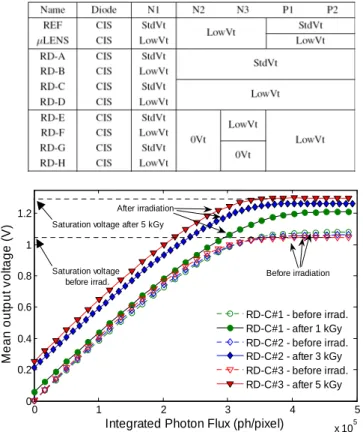
Ten 128x128-3T-pixel-CMOS image sensors, with different designs, have been manufactured and tested, before and after being irradiated with 60Co γ-rays. Several combinations of transistor threshold voltages (Vt) –– standard (SdtVt), low Vt (LowVt) and zero Vt (0Vt) –– have been used to design the sensor readout chains as illustrated in Tab. 1. N1, N2 and N3 are the in-pixel reset, source follower and switch N channel MOSFETs. After the double sample and hold stage, two simple switched P-MOST source followers are used at the bottom of each column. In Tab. 1, P1 and P2 represent the source follower P-MOST and the switch P-MOST respectively. One sensor (µLENS) has a microlens array on top. All the manufactured CIS have a 10 µm pixel pitch and a conversion factor around 8 µV/e-, except the µLENS sensor which has a 7µm pixel pitch and a conversion factor about 14 µV/e-.
III. OPTOELECTRICAL TRANSFER FUNCTION
For 650 nm photon wavelength, the two main radiation effects that can be seen on the optoelectrical transfer function after exposure to γ-rays (Fig. 1) are a dark current rise and a saturation voltage increase.
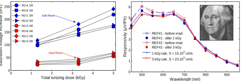
Fig. 2 shows that the main part of the saturation voltage increase is mitigated when the photodiode is reset with a reset MOSFET drain voltage of 2.4V (hard reset) instead of the regular 3.3V used in soft reset mode. In soft reset mode, the photodiode voltage reached at the end of the charge cycle depends on the reset MOSFET characteristics (threshold voltage and subthreshold current) whereas it is not the case in hard reset mode. It can then be inferred that
the largest part of the saturation voltage increase is due to the variation of reset MOSFET threshold voltage and/or subthreshold current. Both these degradations can be attributed to shallow trench isolations according to previous work [6, 7].
Fig. 3 shows a minimum size N channel MOS transistor subthreshold characteristics for two drain to source voltages (VDS) (0.5V and 3.3V) before and after 1 kGy irradiation. During the exposure to γ-rays, this transistor was pulsed in the same conditions than N1 MOSFET of the tested CIS. As expected from the sensor degradations, total ionizing dose led to a significant leakage current increase and a small threshold voltage decrease in the device. It is important to notice that the radiation induced subthreshold leakage current rises significantly when the drain to source voltage increases. VDS is lower when low Vt reset MOST is used instead of a standard Vt MOST. It can explain why sensors with standard Vt N1 (RD-A and RD-C) exhibit a larger saturation voltage increase in soft reset mode (Fig. 2) in comparison to CIS with low Vt N1 (RD-B and RD-D). In hard reset mode, standard Vt and low Vt reset MOSFETs behave the same since the reached reference voltage does not depend anymore on N1 threshold voltage and leakage current.
Optoelectrical Performance Evolution of CMOS
Image Sensors Exposed to Gamma Radiation
V. Goiffon, M. Estribeau and P. Magnan
ISAE, 10 avenue Edouard Belin, 31055 Toulouse
Email:
[email protected]
, Phone: +33 5 6133 8093
TAB.1SUMMARY OF STUDIED SENSOR COMPOSITIONS.
Fig. 1. Opto-electrical transfer function at 650 nm before irradiation, after 1 kGy, after 3 kGy and after 5 kGy.
0 1 2 3 4 5 x 10⁵ 0 0.2 0.4 0.6 0.8 1 1.2
Integrated Photon Flux (ph/pixel)
M e a n o u tp u t v o lta g e ( V ) RD-C#1 - before irrad. RD-C#1 - after 1 kGy RD-C#2 - before irrad. RD-C#2 - after 3 kGy RD-C#3 - before irrad. RD-C#3 - after 5 kGy Saturation voltage after 5 kGy
Saturation voltage before irrad.
Before irradiation After irradiation
2
IV. SPECTRALRESPONSIVITY
Above 1 kGy and below wavelength of 650 nm, ionizing radiations degrade significantly the tested image sensors responsivity as illustrated in Fig. 4. This degradation can be due to an interface state density increase, yielding to a surface recombination velocity increase, as mentioned by [3].The result of an elementary simulation which estimates the effect of a radiation induced enhancement of the surface recombination velocity is also shown in Fig. 4.
The good agreement between the data and the model strongly suggests that surface recombination enhancement, due to the generation of interface states, is most likely the only cause of this observed degradation. However, others phenomena can also explain this wavelength dependent responsivity degradation, such as the creation of color centers [8] in oxides as suggested in [4]. This may bring about a modification of the superficial layer stack transmission. Similar results can be observed on irradiated CIS with microlenses (Fig. 5). As for the REF#1 device, the responsivity at 450 nm is about 12% less after 1kGy irradiation. It suggests that, up to 1 kGy, microlenses optical transmission does not seem to be degraded by the γ-rays.
Latest results, obtained on the RD-D device after 5 kGy irradiation (Fig.6), show a decrease of the responsivity up to 20% at 400 nm (and 14% at 450 nm). Further characterizations on other devices are planned is the next future.
V. DARK CURRENT
As mentioned previously, the dark current rises greatly with total ionizing dose (Fig. 7). The linear dark current density increase is very sharp in comparison to the relatively low dark current density before exposure (4 aA/µm).
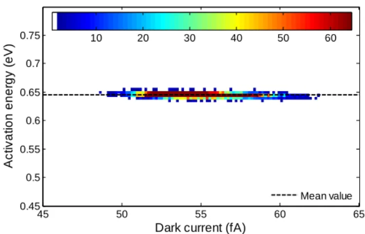
According to previous work [5], this radiation induced dark current is a generation current proportional to the perimeter and is due to the surrounding STI. This is confirmed by the dark current activation energy extraction presented in Fig. 8 and Fig. 9. Before irradiation (Fig. 8), the large activation energy spreading suggests more complex mechanisms than a pure ideal generation current due to midgap centers. A slight electric field enhancement [9], a non uniform defect energy distribution or a significant diffusion current contribution [10] could explain the observed distribution. After 1 kGy (Fig. 9), the activation energy distribution converge clearly around 0.65 eV which is close to the value usually observed for pure radiation induced generation current in irradiated silicon devices (0.63 eV) [1].
VI. CONCLUSION AND FUTURE WORK
Despite the intrinsic hardness of deep submicron MOSFET gate oxides due to their reduced thickness, image sensors manufactured in deep submicron CMOS technologies still exhibit significant degradations when
Fig. 2 Saturation voltage increase with irradiation for two reset modes: soft reset (SR) with VRST = 3.3V and hard reset (HR) with VRST
0 1 2 3 4 5 0 50 100 150 200 250
Total ionizing dose (kGy)
S a tu ra ti o n v o lt a g e i n c re a s e ( m V ) RD-A SR RD-B SR RD-C SR RD-D SR RD-A HR RD-B HR RD-C HR RD-D HR Hard Reset Soft Reset
Fig. 3 N1 MOST subthreshold characteristics before and after 1 kGy for VDS = 0.5 V and 3.3 V. -0.5 0 0.5 1 1.5 2 10-15 10-14 10-13 10-12 10-11 10-10 10-9 10-8 10-7 10-6 10-5 10-4
Gate to source voltage (V)
D ra in c u rr e n t (A ) Before irrad., VDS = 0.5V Before irrad., VDS = 3.3V After 1 kGy, VDS = 0.5V After 1 kGy, VDS = 3.3V
Fig. 4. Responsivity of REF devices prior to and after irradiation and image captured with the 3 kGy irradiated device. The estimated surface recombination effect on responsivity after irradiation is also shown. 500 600 700 800 900 0 1 2 3 4 5 6 Wavelength (nm) R e s p o n s iv it y ( µ V /P h )
REF#1 - before irrad. REF#1 - after 1 kGy REF#2 - before irrad. REF#2 - after 3 kGy
1 kGy calc. S = 15.103 cm/s
3 kGy calc. S = 23.103 cm/s
Fig. 5. Responsivity of the image sensor with microlenses prior to and after 1 kGy irradiation and image captured with the irradiated device.
500 600 700 800 900 0 2 4 6 8 10 12 Wavelength (nm) R e s p o n s iv it y ( µ V /P h
3
exposed to ionizing radiations. The dark current and the saturation voltage rose in the tested sensors, and these effects were attributed to the shallow trench isolations. Such effects can be mitigated in MOSFETs by the use of enclosed layout transistors and their use is recommended for total ionizing doses greater than 1 kGy. In terms of responsivity, a wavelength dependent decrease is observed on image sensors, with or without microlenses. This can be due to an increase of surface recombination velocity, as shown by our elementary simulation, and/or a change in the superficial layers stack transmittance. As regards the dark current, radiation hard photodiodes which can be used in any commercial deep submicron CIS process are still under study.
These results are likely to be transposable to 4T pinned photodiode based CIS. In order to confirm this point, such devices are being characterized for similar irradiation tests.
REFERENCES
[1] G. R. Hopkinson, “Radiation effects in a CMOS active pixel sensor,” IEEE Trans. Nucl. Sci., vol. 47, no. 6, pp. 2480–2484, Dec. 2000. [2] B. R. Hancock, T. J. Cunningham, K. P. McCarty, G. Yang, C. J.
Wrigley, P. G. Ringold, R. C. Stirbl, and B. Pain, “Multi-megarad (Si) radiation tolerant integrated CMOS imager,” in Proc. of SPIE, vol. 4306, 2001, pp. 147–155.
[3] J. Bogaerts, B. Dierickx, G. Meynants, and D. Uwaerts, “Total dose and displacement damage effects in a radiation-hardened CMOS APS,” IEEE Trans. Electron Devices, vol. 50, no. 1, pp. 84–90, Jan. 2003.
[4] P. R. Rao, X. Wang, and A. J. P. Theuwissen, “Degradation of CMOS image sensors in deep-submicron technology due to γ-irradiation,” Solid-State Electron., vol. 52, no. 9, pp. 1407–1413, Sep. 2008.
[5] V. Goiffon, P. Magnan, O. Saint-Pé, F. Bernard, and G. Rolland, “Total dose evaluation of deep submicron CMOS imaging technology through elementary device and pixel array behavior analysis,” IEEE Trans. Nucl. Sci., vol. 55, no. 6, Dec. 2008.
[6] H. J. Barnaby, “Total-ionizing-dose effects in modern CMOS technologies,” IEEE Trans. Nucl. Sci., vol. 53, no. 6, pp. 3103–3121, Dec. 2006.
[7] F. Faccio and G. Cervelli, “Radiation-induced edge effects in deep submicron CMOS transistors,” IEEE Trans. Nucl. Sci., vol. 52, no. 6, pp. 2413–2420, Dec. 2005.
[8] Fernandez-Rodriguez, M., Alvarado, C., Nunez, A. and Alvarez-Herrero, A. "Modeling of Absorption Induced by Space Radiation on Glass: A Two-Variable Function Depending on Radiation Dose and Post-Irradiation Time," IEEE Trans. Nucl. Sci., vol. 53, no. 4, pp. 2367–2375, Aug. 2006
[9] J. R. Srour et R. A. Hartmann, “Enhanced displacement damage effectiveness in irradiated silicon devices,” IEEE Trans. Nucl. Sci., vol. 36, num. 6, p. 1825-1830, Dec. 1989.
[10] N. V. Loukianova, H. O. Folkerts, J. P. V. Maas, D. W. E. Verbugt, A. J. Mierop, W. Hoekstra, E. Roks, et A. J. P. Theuwissen, “Leakage current modeling of test structures for characterization of dark current in CMOS image sensors,” IEEE Trans. Electron Devices, vol. 50, num. 1, p. 77-83, 2003.
Fig. 7. Radiation induced dark current linear density increase as a function of total ionizing dose at 23°C. Junction perimeter = 35µm.
10-1 100
10-2 10-1 100 101
Total ionizing dose (kGy)
D a rk c u rr e n t in c re a s e ( fA /µ m ) data fit 1.6 x1.4
Fig. 6. Responsivity of the RD-D sensor prior to and after 5 kGy irradiation. 400 500 600 700 800 900 0 1 2 3 4 5 6 Wavelength (nm) R e s p o n s iv it y ( µ V /P h ) RD-D#3 - before irrad. RD-D#3 - after 5 kGy
Fig. 8. Dark current activation energy versus dark current measured at room temperature before irradiation.
Dark current (fA)
A c ti v a ti o n e n e rg y ( e V ) 0 0.05 0.1 0.15 0.2 0.25 0.3 0.35 0.4 0.45 0.5 0.55 0.6 0.65 0.7 0.75 10 20 30 40 50 60 Mean value
Fig. 9. Dark current activation energy versus dark current measured at room temperature after 1 kGy.
Dark current (fA)
A c ti v a ti o n e n e rg y ( e V ) 45 50 55 60 65 0.45 0.5 0.55 0.6 0.65 0.7 0.75 10 20 30 40 50 60 Mean value