$Q\FRUUHVSRQGHQFHFRQFHUQLQJWKLVVHUYLFHVKRXOGEHVHQWWRWKHUHSRVLWRU\DGPLQLVWUDWRU WHFKRDWDR#OLVWHVGLIILQSWRXORXVHIU
2SHQ$UFKLYH7RXORXVH$UFKLYH2XYHUWH2$7$2
2$7$2 LV DQ RSHQ DFFHVV UHSRVLWRU\ WKDW FROOHFWV WKH ZRUN RI VRPH 7RXORXVH UHVHDUFKHUVDQGPDNHVLWIUHHO\DYDLODEOHRYHUWKHZHEZKHUHSRVVLEOH
7KLVLVYHUVLRQSXEOLVKHGLQ
7RFLWHWKLVYHUVLRQ
2IILFLDO85/
an author's https://oatao.univ-toulouse.fr/11393
https://doi.org/10.1109/TNS.2010.2085448
Virmontois, Cédric and Goiffon, Vincent and Magnan, Pierre and Girard, Sylvain and Inguimbert, Christophe and Petit, Sophie and Rolland, Guy and Saint-Pé, Olivier Displacement Damage Effect Due to Neutron and Proton Irradiations on CMOS Image Sensors Manufactured in Deep Sub-Micron Technology. (2010) In: 2010 IEEE
International Nuclear and Space Radiation Effects Conference (NSREC), 19 July 2010 - 23 July 2010 (Denver, United States).
Displacement Damage Effects Due to Neutron and Proton Irradiations on CMOS Image Sensors
Manufactured in Deep Submicron Technology
Cedric Virmontois, Student Member, IEEE, Vincent Goiffon, Member, IEEE, Pierre Magnan, Member, IEEE, Sylvain Girard, Member, IEEE, Christophe Inguimbert, Sophie Petit, Guy Rolland, and Olivier Saint-Pé
Abstract—Displacement damage effects due to proton and neutron irradiations of CMOS image sensors dedicated to imaging are presented through the analysis of the dark current behavior in pixel arrays and isolated photodiodes. The mean dark current in- crease and the dark current nonuniformity are investigated. Dark current histogram observations are compared to damage energy distributions based on GEANT 4 calculations. We also discuss, through annealing analysis, which defects could be responsible for the dark current in CMOS image sensors.
Index Terms—Active pixel sensor (APS), CMOS image sensor (CIS), displacement damage, hot pixels, ionization, monolithic ac- tive pixel sensor (MAPS), non-ionizing energy loss (NIEL).
I. INTRODUCTION
D
ISPLACEMENT DAMAGE EFFECTS on CMOS image sensors (CIS) dedicated to space applications have been studied for several years [1]–[4]. In the space radiation environ- ment, -rays, electrons, protons and high energy particles im- pinge electronic devices, interact with them and alter their elec- trical properties. It is well established [5] that the radiation-in- duced damages can be separated into two phenomena: ioniza- tion effects and displacement damage effects.Ionization, the most studied mechanism in CIS [1]–[3], [6], creates charges along the particle track leading to the generation of trapped charges and interface states at the interface.
For charged particles, Ionization effects are quantified using the linear energy transfer (LET) [7] which allows the evaluation of the total ionizing dose (TID) absorbed by the silicon and the silicon oxide layers. Previous TID studies on CIS pixel arrays and test structures [8] demonstrated that the main part
C. Virmontois, V. Goiffon, and P. Magnan are with the Université de Toulouse, ISAE, 31055 Toulouse, France (e-mail: [email protected];
[email protected]; [email protected]).
S. Girard is with the CEA, DAM, DIF, F91297 Arpajon, France (e-mail: syl- [email protected]).
C. Inguimbert is with the ONERA DESP, 31055 Toulouse, France (e-mail:
S. Petit and G. Rolland are with the CNES, 31401 Toulouse, France (e-mail:
[email protected]; [email protected]).
O. Saint-Pé is with the EADS Astrium, 31402 Toulouse, France (e-mail:
of the TID induced dark current increase comes from the pho- todiode perimeter. The photodiode is surrounded by shallow trench isolation (STI) where the trapped charges and the in- terface states are located. These defects, along the photodiode perimeter, are directly in contact with the photodiode space charge region which leads to a dark current dominated by the Shockley-Read-Hall generation [9].
Displacement damage effects in active pixel sensor (APS) are a subject of ongoing research. Displacement effects occur when a particle passes through the semiconductor. It can in- teract with atom nucleus through columbic or nuclear interac- tions which can displace them from there normal position in the lattice creating defects. The collision can be elastic or in- elastic and the interaction cross section depends on the particle energy [10]. After irradiation, a large amount of interstitial/va- cancy defects, Frenkel pairs, are created but most of these will recombine [11]. The non-recombined defects move thanks to a diffusion mechanism leading to stable defects. These defects can be intrinsic or at sites of dopants and/or impurities.
In APS, point defects or clusters of defects located in the pho- todiode space charge area increase the mean dark current and the dark current distribution through generation mechanism. In- deed, these damages lead to energy levels within the band gap and form dark signal generation centers. This generation current could be enhanced through electric field [3], [4]. The damages due to displacement could also increase the random telegraphic signal noise in pixels [12]. Displacement damage effect on dark current in silicon based optoelectronic device is know to scale with the rate of non-ionizing energy loss (NIEL) [11, and refer- ences therein] throught the universal damage factor [13].
In this paper, we study displacement damage effects on CMOS image sensors processed in a deep submicron (DSM) technology dedicated to imaging. Previous studies on this technology have highlighted the sensor behavior against -rays and proton irradiations [8]. These studies show that TID does not degrade significantly the electro-optic parameters but increases dramatically the dark signal leading to a sensor dynamics drop. It was seen that the dark current is a generation current and no significant electric field enhancement (EFE) effect was observed. After the proton irradiations, both ionizing and displacement effects were observed, but the displacement damages could not be properly studied because of TID effect dominance. Indeed, after proton irradiations, the mean dark current relative to ionization was one order of magnitude higher than the one due to displacement. However, the displacement damage was responsible of the dark current nonuniformity
Fig. 1. Schematic diagram of the pixel unit cell.
increase and the creation of hot pixels. Theses damages present a critical performance issue for CMOS image sensors that are used in space applications, especially when the sensors operate at low light levels. The solution developed in this paper to study properly displacement damages is to use neutral particles which induce negligible ionization. Based on the correlation between neutron and proton irradiations regarding displacement effect in silicon [14], [15] we use neutron irradiations to compare, for the first time in APS, the displacement damage due to neutron and proton irradiations.
First, we describe the sensors that are used for this study as well as neutron and proton exposures they underwent. Second, we illustrate proton and neutron irradiation damages in APS, revealed by measurements on isolated photodiodes with dimen- sion variations and by mean dark current measurement on pixel arrays. Third, we examine the dark current nonuniformity and we focus on the hot pixel tail generally attributed to inelastic collisions and/or electric field enhancement [4]. We propose a formalism, based on the microvolume theory [16]–[18], to ex- plain the dark current nonuniformity. It is based on the propor- tionality between the dark current distribution and the deposited damage energy in pixel microvolumes. This formalism is used for the first time after neutron irradiations in CIS, and in our case, the GEANT 4 code is used to estimate the energy recoil spectrum and the induced damage energy distribution due to neutron irradiations. This formalism is then transposed to the results obtained after proton irradiations to compare the dis- placement damage effects in both cases. Finally, an isochronal annealing analysis is presented to compare the dark current de- creases in pixel arrays and in isolated photodiodes allowing a better understanding of the defects in APS after irradiations.
II. EXPERIMENTALDETAILS
Several 128 128 pixel arrays (3T configuration [19] with pitch) and more than 20 isolated test photodiodes with implant and dimension variations were designed on the test chips. Fig. 1 shows a schematic diagram of a 3T pixel.
These circuits were manufactured using a commercial CMOS technology dedicated to imaging applications. This technology is based on a P lightly doped epitaxial layer grown on a P conductive substrate layer.
Current-voltage measurements were carried out at room tem- perature using a low-current test bench specially de-
TABLE I
IRRADIATIONCHARACTERISTICS
signed for these measurements and described more in detail in [9].
The circuits were exposed to a neutron beam at the Université Catholique de Louvain (UCL) facility and CEA DAM Valduc site. Proton beam tests were realized at Vancouver (TRIUMF), at the Kernfysisch Versneller Instituut (KVI) and at the UCL.
The total displacement damage dose (DDD) ranged from 34 to 365 TeV/g and up to 20000 TeV/g for one chip. Table I de- scribes the irradiations which were performed at room temper- ature. Dosimetry is considered to be accurate to better 5% at the UCL and CEA DAM Valduc facilities. The measurements that are shown in this paper were performed approximately three weeks after irradiation.
An isochronal annealing analysis is performed on all the de- vices after the first measurement. During this analysis the tem- perature ranged from 80 C to 280 C. The circuits were oven- baked 30 minutes at each temperature step. And the temperature step was 40 C. We adjusted the integration time and the gain at each step to measure accurately the pixels response for normal and hot pixel (i.e., to keep normal and hot pixel dark signal in the linear range of the sensor). All these measurements were carried out at room temperature after each annealing step.
III. PROTON ANDNEUTRONDAMAGEANALYSIS
Protons, thanks to their intrinsic positive charge, induce at the same time ionization and displacement effects. Evaluation of the relative impact of each effect is then difficult. In the case of neutron (which carries no charge) such ionization effects are negligible. Proton and neutron NIEL are close on the energy range of interest for space applications, i.e., in the same half decade for energy ranging from 10 to 100 MeV. However, proton and neutron interactions are different. Protons create important ionization through columbic interaction with electron clouds whereas neutrons are not influenced by the electron charge. However, both hadrons can interact with nucleus and create primary knock-on atoms (PKA). PKA is most of the time a silicon atom or ion that can also ionize the lattice and displace atoms. Compared to the direct proton ionization, the PKA ionization is negligible. Indeed, thanks to SRIM software calculation, for silicon or silicon oxide exposed to 10 MeV pro- tons the direct total ionization is two orders of magnitude above
Fig. 2. (1) Main defects leading to dark current increase after-ray, (2) proton, and (3) neutron irradiation in pixel photodiode.
the one obtained from the PKAs. Fig. 2 illustrates in-pixel pho- todiode defects after -ray, proton and neutron irradiations. The main defects responsible for the dark current are drawn. The red crosses represent interface states and trapped charges due to ionization effects (induced by -ray and proton irradiations).
The blue circles represent point defects or clusters of defects due to displacement damages. Such defects are generated in silicon bulk after proton and neutron exposures.
Proton and neutron interactions are different [11] but several studies reveal identical electronic property damages in solid state sensor based on silicon [13]. This can be attributed to defects and clusters of defects reorganizations after irradiation leading to the same stable electronic damages. A universal damage factor (UDF) was established by Srour [13] to estimate the dark current relatively to displacement damages. This factor is independent on the use of proton or neutron and on the impurities and dopant present inside the silicon. This suggests that dark current comes from defects based on multi-vacancy and/or other intrinsic lattice flaws.
Fig. 3(a) and (b) show mean dark current increase in pixel arrays after proton and neutron irradiation following a displace- ment damage dose. The red line corresponds to the dark current estimated thanks to the UDF
(1) where q is elementary charge, is the UDF equal to at 300 K, is the depleted volume. To minimize the error on it we performed TCAD simulation to obtain the most realistic depleted volume. Sec- ondary ion mass spectroscopy (SIMS) was used to estimate the real doping profiles necessary for the TCAD simulation.
One can see in the figure that the mean dark current increase
Fig. 3. Mean dark current increase after (a) proton and (b) neutron irradiation following Displacement damage dose.
after proton irradiation is one order of magnitude higher than the one estimated through (1). The measurements performed after neutron irradiations, even for high displacement damage dose (DDD), are in good agreement with simulations. For these devices, the dark current increases due to total ionizing dose are significantly higher than the dark current increases due to displacement damages. This effect demonstrates the difficulties associated with the analysis of displacement damage impact on the dark current characteristics when the APS is irradiated by protons. The good agreement with neutron validates the UDF for the studied APS.
In order to understand the origin of the dark current, sev- eral photodiodes with dimension variations have been irradiated and characterized. The reverse current at 2.4 V (photodiode bias after the reset phase in a standard CIS operating mode) is divided by the photodiode surface and plotted versus the perimeter over surface ratio, given this equation
(2) (3) where is the perimeter, is the surface, is the perimeter contributions and is the surface contributions.
Fig. 4 presents this method. The slopes represent the perimeter contributions and the axis intersection, the surface contributions. Table II illustrates this analysis for different irra- diation conditions. Perimeter and surface dark current increase contributions referred to the in pixel photodiode dimension are presented (“% Idark Perimeter” and “% Idark Area”). In-pixel
Fig. 4. Photodiode reverse current at 2.4 V after irradiation illustrating perimeter and area contribution of the current.
TABLE II
DARKCURRENTANALYSISAFTERIRRADIATION ON PHOTODIODEWITHDIMENSIONALVARIATION
photodiode, dark current is extrapolated thanks to the large pho- todiodes and is compared to the measured mean dark current in pixel arrays. It can be seen that both are in good agreement. For -rays, the contribution comes essentially from the perimeter, emphasizing the role of interface states and trapped charges in STI due to ionization. These results also demonstrate that a negligible number of defects are created in silicon bulk. In the neutron case, defects are distributed in the entire volume, so the area contribution is higher than the one of the perimeter.
Estimated perimeter and area dark current contributions are close to the depleted region perimeter and surface proportions, showing that defects are distributed in all the photodiode.
Neutron irradiations induce essentially displacement damage.
For proton, we clearly see the impact of the perimeter, showing the important contribution of ionization effects. As regards the surface contribution, it is not negligible, which suggests the presence of silicon bulk defect mainly due to displacement damage. This helps to analyze the dark signal distribution presented in Fig. 5. Indeed the dark current distribution after the proton irradiation presents a Gaussian shape followed by a tail of hot pixels generally attributed to displacement damages.
At the opposite, for -ray irradiations (with only ionization),
Fig. 5. Dark current distribution after proton and neutron irradiation at the same displacement damage dose.
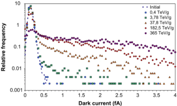
Fig. 6. Dark current distributions after neutron irradiations at different dis- placement damage doses.
the distribution would be Gaussian [8]. In the proton case, the Gaussian mean is shifted from its initial position because of the uniform TID effect. Dark current distribution fit based on Normal law is presented in [8] for this sensor. The dark current Gaussian distribution mean and variance are shown to increase with total ionizing dose following second order poly- nomial laws. Fig. 5 also shows the distribution after neutron irradiations, the Gaussian part stays at the same place as for the non-irradiated device as there is a negligible ionization effect.
For DDD presented in this figure, the displacement damage occurrence per pixel is not sufficient to impact all the pixels.
For this reason, after a neutron irradiation, most of the pixel dark current stays unchanged and the pixel tail represents the number of displacement interactions on the pixel arrays. Fig. 6 illustrates the proportional evolution of the tail with the DDD.
We have shown in this part the similarities between protons and neutrons regarding displacement damage effects. Despite the fact that neutron irradiations are not the particles represen- tatives of space mission environment, they appear to be an inter- esting tool to study properly the DDD in APS. These irradiations allow us to understand better the displacement phenomenon in APS. This understanding can then be used to analyze proton irradiation results (which are more representative of the space radiation environment).
IV. DARKSIGNALNONUNIFORMITYANALYSIS
A. Analytical Model
Previous work on neutron damaged APS [20] showed that the dark current spikes increase with fluence. Fig. 6 illustrates this increase following DDD. When DDD goes up, the number of defects increases bringing more dark current. But, as explained before, for space fluence range, not all pixels are impacted by displacement. For this reason, even at maximum fluence, some pixels do not exhibit a dark current increase. Defects due to displacement damages are created in the entire sensor but only those located in the photodiode space charge region have a no- ticeable impact on the dark current. This area is considered as a microvolume and neutron interactions do not necessarily occur in each one. The neutron cross section, obtained with GEANT 4 code allows to calculate the average number of interaction per microvolume
(4) where is the fluence, is the interaction cross section, is the number of silicon atom per volume and is the de- pleted volume. For the fluence of interest, the average number of events per microvolume is not sufficient to predict a Gaussian distribution of event in pixels. It suggests a discrete Poisson dis- tribution of all recoils throughout the pixels [16].
(5) where is the number of events and the average number of events in a microvolume.
GEANT 4 code simulates the neutron interaction of
silicon. The results obtained are the energy of each target parti- cles.
Contrary to proton studies [3], [16]–[18], neutron elastic and inelastic cross sections are close and a separation of both inter- action types is not necessary. Indeed, the number of pixels in the tail is proportional to the probability of having at least one event per microvolume. If we consider only inelastic cross sec- tion, the calculated probability is under the percentage of pixels inside the pixel tail. However, when all interactions, provided by GEANT 4, are taken into account, we obtain a correct agree- ment between the number of pixel in the tail and the probability of having at least one event. This means that all nuclear interac- tions, elastic and inelastic, contribute to the dark current spikes.
0.8 MeV neutrons only lead to nuclear elastic interactions. In- elastic cross section is null at this energy. We can see in Fig. 3 that 0.8 MeV neutron induced dark current follows the UDF.
We can then infer that nuclear elastic events have to be taken into account for the estimation of the dark current distribution.
An analytic model of dark current increase based on Marshall work [16]–[18], can be derived using the proportionality with damage energy imparted by a particle. Previous studies [16]
compared the dark current increase in CID to damage energy induced through elastic and inelastic proton interaction. In the neutron irradiations case, no difference is made between elastic and inelastic interaction. GEANT 4 provides statistics of recoil element energies. Recoil elements are separated through atomic mass and their damage energy is calculated from their recoil en- ergy using a representation due to Robinson formulation [21] of
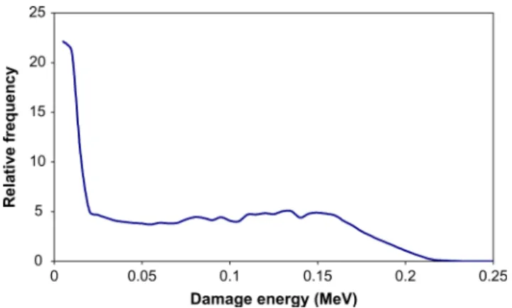
Fig. 7. Normalized mean damage energy communicated to silicon by one re- coil element. Calculations have been based on 15 MeV neutron.
the Lindhard partition function [22]. These equations provide the share of displacement damage energy from particle total en- ergy. The total damage energy distribution from all recoil ele- ments is then obtained and presented in Fig. 7. This defines the mean damage energy communicated to silicon by a recoil ele- ment. Probability formalism is needed to go further in the de- scription of this method. Damage energy from single element is represented by a discrete random variable . Probability den- sity function (PDF), , is associated to this variable and corresponds to Fig. 7. Another discrete random variable, , is used, representing the mean damage energy provided by a re- coil element in a pixel sensitive microvolume. The PDF cor- responding to is calculated as (6). Neutron cross section is calculated and used to obtain the average number of events per microvolume. The average ranges typically from a fraction to a few. This suggests a Poisson distribution for event throughout the array’s microvolume. The PDF associated to , representing the probability of damage in a pixel with a event, reflects the
-fold convolution of the PDF
(6) where is the Kronecker delta equal to 1 if and equal to 0 if . The amount of damage energy received in a pixel is then represented by the PDF corresponding to .
B. Dark Current Increase Due to Neutron Irradiation
The formalism developed above is used to compare predicted damage energy and a measured dark current increase. All dis- tributions are normalized and the average conversion factor of 9.89 fA per MeV is used. It is based on the UDF calculation
(7) where is the damage energy (per microvolume at given a fluence) and is the density of the silicon. Fig. 8 presents the comparison between the measured dark current increase and the analytic model from predicted damage energy. The differ- ence at low dark current could be attributed to the measurement uncertainty.
Indeed, between two measurements, for example pre-irradi- ation and post-irradiation measurements, there is an accuracy
Fig. 8. Comparison between modeled and measured Dark current increase dis- tribution after neutron irradiations at different displacement damage dose. No fit parameter is used.
error leading to a spreading of the first value, normally equal to zero, i.e., with dark current unchanged after irradiation. This is not the case on the predicted curve because of the use of the Kronecker delta effect. For dark current spike a difference be- tween estimated and experimental data is also observed. This difference could be attributed to the use of Gaussian approxi- mation for the PDF associated to . The real distribution of each PDF probably has to be used to obtain a better correlation.
Estimation of dark current increase due to displacement damage is in correct agreement with measurements at several DDD. It reveals the importance of taking into account the nuclear elastic interaction in addition to inelastic event in the evaluation of the total induced damage.
C. Activation Energy
Contrary to [3], no enhancement generation factor is consid- ered in the model. To confirm that there is no electric field en- hancement (EFE) in our pixels, activation energy calculations after neutron and proton irradiations have been performed using dark current measurements from C to C (In this tem- perature range, the main dark current mechanism is the gener- ation in the space charge of the in-pixel photodiode). The pur- pose is to observe the behavior of activation energy on dark cur- rent spike. In the case of EFE a activation energy decrease is observed in high leakage current pixels [4]. Dark current acti- vation energy calculation is based on the relationship between dark current and temperature.
(8) where is the dark current activation energy, is the Boltz- mann constant, the temperature in Kelvin and is a coeffi- cient equal to zero, two or three. In many studies this coeffi- cient is taken to zero to obtain an approximated activation en- ergy. BY doing so, the evolution is neglected in front of the exponential term. The typical value reported using this ap- proximation is 0.63 eV. To go further in detail, we have to take into account the parameters that depend on temperature in the Shockley-Read-Hall generation rate. For surface generation, equal 3 [23] and for bulk volume generation the value is 2. As exposed previously, neutron damages are distributed in the en- tire volume and is then used. For proton, surface gen-
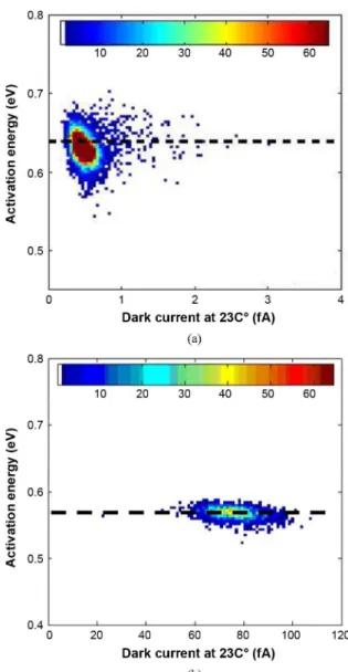
Fig. 9. Activation energy is plotted against dark current at 23 C. (a) Proton irradiation and (b) neutron irradiation at very high fluence not present activa- tion energy decrease for high leakage current. That reveals no electric field enhancement.
eration due to the ionizing effect and volume generation due to the displacement effect occur. To compare with other work, we decided to calculate the approximated dark current activation energy for proton. Fig. 9 represents the dark current activation energies for each pixel plotted against dark current at C.
Both irradiation cases reveal no activation energy decrease for high leakage current pixel. It confirms no EFE effect in our APS.
The use of process CIS dedicated to imaging could explain a controlled electric field smoothing over the photodiode depleted region. Mean value of 0.58 eV is found for neutron with the temperature coefficient considered. Which is close to the ideal mid-gap value (0.56 eV), suggesting a generation mechanism.
As for other studies [18], estimated activation energy of 0.63 eV is found after proton irradiation which also suggests a generation mechanism.
D. Dark Current Increase Due to Proton Irradiation
The analytic model obtained in previous part reveals a cor- rect agreement with APS dark current increase due to displace-
Fig. 10. Comparison between modeled and measured dark current increase dis- tribution after proton irradiations. The proton DDD rise 39 TeV/g.
ment damages only. However, in space environment, neutrons are less in number than proton. Solar flares, cosmic rays and ra- diation belt are mainly composed of proton. So, the damages in- duced during a space mission consist in both displacement and ionizing damages. To predict the dark current increase due to proton, we have to take into account both effects. We have sep- arated the dark current increase in two currents
(9) One is from ionizing damages and the other one is from dis- placement damages. To estimate the dark current increase due to proton, we associate random variables and PDF to each pa- rameter of (8). The PDF associated to displacement current is calculated with the previous model for a given DDD. The PDF associated to ionizing current is obtained using the fit model in [8] for a given TID. Both variables are considered independent because dark current generated from interface states in STI are independent of those generated from bulk defect in the space charge area of the photodiode. Finally, the estimated total dark current increase distribution is the convolution of both previous PDF. Fig. 10 compares estimated and measured dark current in- creased after proton irradiation. Both curves are close, excepted around 2 fA, there is a bump on the simulation curve. This Bump is also observed on Fig. 7 for the same DDD. We do not know exactly to which this distortion is attributed but, when we look at damage energy of each recoil element, it may be due to re- coil element which can be induce by elastic or inelastic interaction. To improve the model, a particular attention to each element has to be considered.
V. ANNEALING OFDARKCURRENT
A. Photodiodes and Pixel Arrays Comparison
Isochronal annealing is usually performed to study the an- nealing of point defects [24]. We chose to perform such anal- ysis on pixel arrays and photodiode in order to compare dark current annealing with defect annealing. It allows the identifi- cation of defects responsible for dark current increase. Studies of radiation damage in silicon particle detectors [25] point out that only intrinsic defects, composed of vacancies and intersti- tials, are responsible for dark current increase. A more recent
Fig. 11. Annealing behavior of the pixel tail after neutron irradiation at 39 TeV/g.
Fig. 12. Unannealed factor obtain after 40 annealing step from 80 C to 280 C on photodiodes and pixel arrays which received different DDD with neutrons.
study, [26] showed that the defect inducing the dark current in- crease could be cluster of defects. Indeed, dark current unan- nealed fraction generally decreases slowly with temperature, whereas a steep decrease at the defect annealing temperature is expected for point defects induced degradation. Fig. 11 shows the annealing of dark current increase distribution. The pixel tail is reduced after each annealing and we calculate the unan- nealed fraction of the mean dark current increase. Fig. 12 illus- trates this fraction for several photodiodes and pixel arrays re- ceiving different DDD. One can see that the measured dark cur- rent annealing behavior does not correspond to point defects be- havior, whereas it is similar to clusters of defects behavior. This spreading along the temperature range could be explained by the cluster annealing kinetic [26]. First, defects located around the cluster are annealed, then the defects at the middle, leading to a spreading of the apparent annealing temperature. DLTS mea- surements on cluster of defects are being performed and will be the object of future work.
VI. CONCLUSION
Displacement damage was investigated in CMOS image sensors manufactured in deep submicrometer technology.
Neutron irradiation appeared to be a good method to study properly displacement damage effects. We observe that dark current increase distributions due displacement damage are
proportional to the damage energy provided by incident parti- cles. This damage energy was calculated thanks to GEANT 4 calculations including elastic and inelastic nuclear interactions.
Annealing analysis provided information about the defects created after irradiation which are responsible for dark current increase. These defects are intrinsic and could be in the form of clusters of defects
ACKNOWLEDGMENT
The authors would like to thank the CIMI Group for their help, especially M. Estribeau for data analysis, F. Corbière and S. Rolando for the sensor conception and P. Cervantes for her help in measurements. They would also like to thank TRIUMF’s Committee for providing the proton beam time, S. Quenard, Y.
Leo, CEA, Valduc, and G. Berger, UCL, Belgium, for there as- sistance during neutron irradiation. I would like to thank, in par- ticular, P. Paillet for saving my components from the maze of French post.
REFERENCES
[1] G. R. Hopkinson, “Radiation effects in a CMOS active pixel sensor,”
IEEE Trans. Nucl. Sci., vol. 47, no. 6, pp. 2480–2484, Dec. 2000.
[2] M. Cohen and J.-P. David, “Radiation-induced dark current in CMOS active pixel sensors,” IEEE Trans. Nucl. Sci., vol. 47, no. 6, pp.
2485–2491, Dec. 2000.
[3] J. Bogaerts, B. Dierickx, G. Meynants, and D. Uwaerts, “Total dose and displacement damage effects in a radiation-hardened CMOS APS,”
IEEE Trans. Nucl. Sci., vol. 50, no. 1, pp. 84–90, 2003.
[4] J. R. Srour and R. A. Hartmann, “Enhancement displacement damage effectiveness in irradiated silicon devices,”IEEE Trans. Nucl. Sci., vol.
36, no. 6, pp. 1825–1830, Dec. 1989.
[5] J. R. Srour and J. M. McGarrity, “Radiation effects on microelectronics in space,”Proc. IEEE, vol. 76, no. 11, pp. 1443–1469, Nov. 1988.
[6] E.-S. Eid, T. Y. Chan, E. R. Fossum, R. H. Tsai, R. Spagnuolo, J. Deily, W. B. Byers, and J. C. Peden, “Design and characterization of ionizing radiation-tolerant CMOS APS image sensors up to 30 Mrd (Si) total dose,”IEEE Trans. Nucl. Sci., vol. 48, no. 6, pp. 1796–1806, Dec. 2001.
[7] C. Inguimberg, “Radiation-matter interaction,” inSpace Radiation En- vironment and its Effects on Spacecraft Components and Systems.
Toulouse: Cepadues, 2004, pp. 84–107.
[8] C. Virmontois, I. Djite, V. Goiffon, M. Estribeau, and P. Magnan,
“Proton and-ray irradiation on deep sub-micron processed CMOS image sensor,” inProc. Int. Symp. Reliability of Optoelectronics for Space, ISROS, 2009, pp. 217–222.
[9] V. Goiffon, C. Virmontois, P. Magnan, S. Girard, and P. Paillet, “Anal- ysis of total dose induced dark current in CMOS image sensors from interface state and trapped charge density measurements,”IEEE Trans.
Nucl. Sci., vol. 57, no. 6, pt. 1, Dec. 2010.
[10] J. R. Srour, C. J. Marshall, and P. W. Marshall, “Review of displace- ment damage effects in silicon devices,”IEEE Trans. Nucl. Sci., vol.
50, no. 3, pp. 653–670, Jun. 2003.
[11] G. Hopkinson, “Displacement damage : Analysis and characterization of effects on devices,” inSpace Radiation Environnement and its Ef- fects on Spacecraft Components and Systems. Toulouse: Cepadues, 2004, pp. 175–197.
[12] I. H. Hopkins and G. R. Hopkinson, “Random telegraph signals from proton-irradiated CCDs,”IEEE Trans. Nucl. Sci., vol. 40, no. 6, pp.
1567–1574, Dec. 1993.
[13] J. R. Srour and D. H. Lo, “Universal damage factor for radiation-in- duced dark current in silicon devices,”IEEE Trans. Nucl. Sci., vol. 47, 2000.
[14] G. P. Summers, E. A. Burke, C. J. Dale, E. A. Wolicki, P. W. Marshall, and M. A. Gehlhaussen, “Correlation of particle-induced displacement damage in silicon,”IEEE Trans. Nucl. Sci., vol. NS-34, Dec. 1987.
[15] J. P. Raymond and E. L. Petersen, “Comparaison of neutron, proton and gamma ray effects in semiconductor devices,”IEEE Trans. Nucl.
Sci., vol. NS-34, no. 6, pp. 1133–1139, Dec. 1987.
[16] P. W. Marshall, C. J. Dale, E. A. Burke, G. P. Summers, and G. E.
Bender, “Displacement damage extremes in silicon depletion regions,”
IEEE Trans. Nucl. Sci., vol. 36, no. 6, pp. 1831–1839 , Dec. 1989.
[17] P. W. Marshall, C. J. Dale, and E. A. Burke, “Proton-induced displace- ment damage distributions and extremes in silicon microvolumes,”
IEEE Trans. Nucl. Sci., vol. 37, no. 6, pp. 1776–1783, Dec. 1990.
[18] M. S. Robbins, “High-energy proton-induced dark signal in silicon charge coupled devices,”IEEE Trans. Nucl. Sci., vol. 47, no. 6, pp.
2473–2479, Dec. 2000.
[19] E. R. Fossum, “CMOS image sensors: Electronic camera-on-a-Chip,”
IEEE Trans. Electron Devices, vol. 44, pp. 1689–1698, Oct. 1997.
[20] A. M. Chugg, R. Jones, M. J. Moutris, J. R. Armstrong, D. B. S. King, and N. Moreau, “Single particle dark current spikes induced in CCDs by high energy neutrons,”IEEE Trans. Nucl. Sci., vol. 50, no. 6, pp.
2011–2017, Dec. 2003.
[21] M. Robbinson, “The dependence of radiation effects on the primary recoil energy,” inProc. Int. Conf. Radiation-Induced Voids in Metal, Albany, NY, 1972, pp. 397–429.
[22] J. Lindhard, V. Nielsen, M. Scharff, and P. V. Thomsen, “Integral equa- tions governing radiation effects (Notes on atomic collisions, III),”Mat.
Fys. Medd. Dan. Vid. Selsk., vol. 33, no. N10, pp. 1–42, 1963.
[23] G. Hopkinson, “Radiation-induced dark current increase in CCDs,” in Proc. 2nd Eur. Conf. Radiation and its Effects on Components and Systems, RADECS 93, Sep. 13–16, 1993, pp. 401–408.
[24] G. D. Watkins, “Intrinsic defects in silicon,”Mater. Sci. Semiconduct.
Process., vol. 3, pp. 227–235, 2000.
[25] M. Moll, “DESY-THESIS-1999-040,” Ph.D. dissertation, Univ. Ham- burg, Hamburg, Germany, 1999.
[26] J. W. Palko and J. R. Srour, “Amorphous inclusions in irradiated silicon and their effects on material and device properties,”IEEE Trans. Nucl.
Sci., vol. 55, no. 6, pp. 2992–2999, Dec. 2008.