To cite this version :
Goiffon, Vincent
Radiation Effects on CMOS
Active Pixel Image Sensors.
In: Ionizing Radiation Effects in Electronics. CRC Press, pp.
295-332.
O
pen
A
rchive
T
OULOUSE
A
rchive
O
uverte (
OATAO
)
OATAO is an open access repository that collects the work of Toulouse researchers and makes it freely available over the web where possible.
This is an author-deposited version published in : http://oatao.univ-toulouse.fr/
Eprints ID : 14554
Any correspondance concerning this service should be sent to the repository administrator: [email protected]
1
Radiation Effects on CMOS Active Pixel Image Sensors
Vincent Goiffon
Institut Supérieur de l’Aéronautique et de l’Espace (ISAE-SUPAERO)
Université de Toulouse, France
Table of Content
1 Introduction ... 2
1.1 Context ... 2
1.2 APS, CIS and MAPS ... 2
1.3 Basic knowledge on radiation effects ... 2
2 Introduction to CMOS image sensors ... 3
2.1 Overview of CIS technology ... 3
2.2 Selected important CIS concepts for radiation effect discussions ... 6
2.2.1 Full well capacity and pinning voltage ... 6
2.2.2 Dark current sources ... 8
2.2.3 Random telegraph signal noises: DC-RTS and SF-RTS ... 10
3 Single event effects ... 12
4 Cumulative radiation effects on peripheral circuits ... 12
5 Cumulative radiation effects on pixel performances ... 13
5.1 Total ionizing dose effects ... 13
5.1.1 Degradation mechanism overview and common effects ... 13
5.1.2 Pinned photodiode specific effects ... 17
5.1.3 Radiation-hardening of CIS pixels ... 19
5.2 Displacement damage effects ... 20
5.2.1 Overview ... 20
5.2.2 Dark current, DCNU and RTS... 20
6 Conclusion ... 23
2
1
Introduction
1.1
Context
Today, Complementary-Metal-Oxide-Semiconductor (CMOS) Image Sensors (CIS) [1]–[4], also called Active Pixel Sensors (APS), are the most popular imager technology with several billions manufactured every year [5], [6]. They represent about 90% of the imager market and should exceed 95% in a couple of years [5]. Compared to the main alternative imager technology, the Charge Coupled Device (CCD), CISs have several major benefits such as low-power consumption, high-integration, high speed and the capacity to integrate advanced CMOS functions on-chip (and even inside the pixel). Thanks to the latest technology innovations, CISs are now matching the performances of CCDs in terms of image quality and sensitivity placing them at the forefront even in high-end applications such as digital single-lens reflex, scientific instruments, and machine vision. Thanks to these advantages, CISs are also used in harsh radiation environment for applications such as: space applications, X-ray medical imaging, electron microscopy, nuclear facility monitoring and remote handling (nuclear power plants, nuclear waste repositories, nuclear physics facilities…), particle detection and imaging, military applications etc.. Designing, hardening and testing a sensor for such applications require the understanding of the CIS behavior when exposed to radiation sources. Understanding and improving further the intrinsically good radiation hardness of APS has been a topic of interest since its invention [7]–[13]. This interest has been recently growing with the coming of new behaviors brought by the profound evolution of CIS technologies (as discussed throughout this manuscript) compared to the older generation mainstream CMOS processes used in early work.
The aim of this chapter is to give an overview of the parasitic effects that can undergo a modern CIS when it is exposed to a high energy particle radiation field.
1.2
APS, CIS and MAPS
APS, CIS and Monolithic-Active-Pixel-Sensors (MAPS)[14][15] designate the same type of CMOS Integrated Circuit (IC): a pixel array with a photodetector and an amplifier inside each pixel[1][2]. Depending on the community, one of these names may be used preferentially. APS is the generic term, CIS is mainly used for imaging applications whereas MAPS is the main term used in the particle detection community to emphasize the monolithic nature of the device compared to hybrid detectors. In most of the cases, a CIS is an APS manufactured using a CMOS process optimized for imaging applications (called CIS process) whereas MAPS are generally manufactured using standard, or high voltage CMOS processes and their main purpose is not optical imaging but high energy particle detection (and imaging). From the radiation effect point of view, there is qualitatively no major difference between MAPS and CIS if the photodetector technology is the same. It means that, despite the fact this chapter focuses on CIS, most of the discussions developed here apply to both families of sensors.
1.3
Basic knowledge on radiation effects
The following radiation effect concepts are used in this chapter to describe the influence of high energy particles on CIS. The reader is invited to look at the first chapter of this book or at the references given in this section to have the details of the origin and limitations of these definitions, mechanisms and properties.
When passing through the layers of the materials that constitute an IC, ionizing particles (such as high energy photons (X and γ rays) and charged particles (electrons, protons, heavy ions…)) lose most of their energy by generating electron-hole pairs. This excess of charge carriers can disturb or damage ICs by inducing Single Event Effects (SEE) [16](and references therein) or Total Ionizing Dose (TID) effects. SEE occurs when the electron-hole pairs generated by a single particle are sufficient to disturb or damage the IC whereas TID effects are the result of the cumulative exposure to ionizing radiation.
3
The TID (or absorbed dose) represents the mean energy imparted to matter per unit mass by ionizing interaction and it is expressed here in Gy(SiO2) (i.e. 1J or energy per kg of SiO2)1,2. The ionizing radiation dose
absorbed by electronic circuits in medical and space applications are generally below 100Gy-1kGy whereas the MGy range can be reached in electron microscopes or nuclear and particle physics experiments. Through this chapter the reader should keep in mind that the absorbed TID leads to the buildup of trapped positive charge in the dielectrics, to the buildup of interface states at the Si/oxide interfaces and that these defect densities increase with TID. Detailed review of TID effects can be found in [17]–[22].
High energy particles can also lose their energy in matter through non-ionizing interactions. These interactions can be summarized as direct interactions with atomic nucleus and they generally result in the displacement of this nucleus. Contrary to TID effects that are mainly a concern in dielectrics, atomic displacement is mainly an issue in the crystalline silicon part of the circuit. The effects linked to radiation induced atomic displacements are called displacement damage effects and the mean energy imparted to matter per unit mass by non-ionizing interaction is called Displacement Damage Dose (Dd) (generally expressed in eV/g(Si)). It is important to note that the Dd leads to the creation of defects in silicon lattice that can act as Shockley-Read-Hall (SRH) generation/recombination centers or SRH carrier traps. These defects can take the form of point defects in the lattice or to clusters of defects (also called amorphous inclusions). Reviews of Displacement Damage Effects that discuss the origin and the limitation of the Dd concept (and especially the Non-Ionizing-Energy-Loss(NIEL) concept) can be found in [23]–[26].
2
Introduction to CMOS image sensors
2.1
Overview of CIS technology
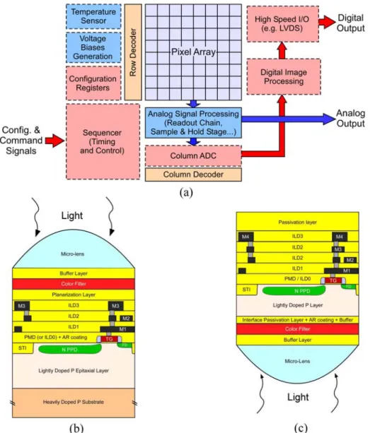
The basic working principle of CMOS Active Pixel Image Sensors can be found in [2], [3], [27]–[30]. As any APS, CIS are constituted by [2] a pixel array, addressing circuits to access the pixels (the address decoders) and an analog signal processing circuit (often called readout circuit). This basic architecture common to nearly every APS IC (including MAPS) is presented in Figure 1a. In addition to these necessary building blocks, modern CIS products [29]–[32] often integrate on-chip one or more of the following functions: one Analog-to-Digital Converter (ADC) per column (see [32]–[34] and references therein for ADC architectures used in CISs), a sequencer, a digital image processing unit, high speed I/O interfaces, configuration registers and so on.
Unlike MAPS that are generally manufactured using standard commercial CMOS processes[35] (standard mixed-mode or high voltage processes, sometimes slightly customized), most of CIS ICs are produced thanks to dedicated CIS processes optimized for visible light detection. Figure 1b and c present simplified cross sectional views of typical modern CIS technologies [36]–[39]. The base of a CIS process is similar to a standard Deep Sub-Micron (DSM) CMOS technology[40]: outside the pixel array, Metal-Oxide-Semiconductor Field-Effect-Transistors (MOSFET) are most often the same as the ones used in the mixed-mode version of the process (i.e. non CIS) with the use of classical Source/Drain implants, N and P wells, Shallow Trench Isolation (STI), polysilicon gates and the typical dielectric stack (constituted by the Inter-Layer Dielectrics (ILD)) on top of the semiconductor devices to insure the isolation between the interconnect layers. The first ILD between the first level of metal and the active silicon or the polysilicon layer is often called the Pre-Metal Dielectric (PMD). Compared to mainstream CMOS ICs, CISs have however several unique features to improve the light collection:
• a reduced number of interconnection metal levels
• dedicated dielectrics such as Anti-Reflection (AR) Coatings
• filters for color imaging
• microlenses and light guides[41][42]
• …
1 Gy(SiO
2) is used here instead of Gy(Si) because TID effects are due to the absorbed dose in the dielectrics (mainly
constituted by SiO2) not to the absorbed dose in the silicon. 2
4
Several improvements are also made at the device level to optimize the photo-generated charge collection while reducing the dark signal and the noise:
• dedicated photodiode and in-pixel isolation doping profiles (P-wells, trench sidewall passivation…)
• dedicated pixel devices (optimized in-pixel MOSFETs with specific threshold voltages, dedicated MOSFET devices for in-pixel charge transfer…)
• a lightly doped epitaxial layer with a thickness optimized for the targeted wavelength range
• dedicated in-pixel trench isolations to minimize crosstalk [43], such as Deep Trench Isolation (DTI)
• …
In addition to these special features, CIS can be Front-Side Illuminated (FSI) or Back-Side Illuminated (BSI), as illustrated in Figure 1b and c. BSI technologies allow to collect more light (leading to higher External Quantum Efficiency (EQE)[31]) for a given fill factor but they require the thinning of the sensitive layer down to a few micrometers and the use of backside passivation techniques to reduce signal charge recombination and dark current generation at the back interface[39], [44]–[46].
Figure 1 : Overview of CIS technology: (a) Typical CMOS Image Sensor Integrated Circuit architecture (the dashed blocks are optional and usually, only one type of output is available in a CIS (digital or analog)). Example of FSI (b) and BSI(c) CIS cross sectional views (inspired from the cross sectional view shown in [36]).
5
Several active pixel architectures have been proposed[2] but the vast majority of modern device pixels are based on these two basic designs: the 3T-pixel based on a conventional photodiode (Figure 2a) and the 4T-pixel based on a dedicated buried photodiode (Figure 2b), called Pinned PhotoDiode(PPD) [47]–[50]. Because of its low noise, high quantum efficiency and low dark current[50] the pinned photodiode is used in almost all consumer applications. However, this photodetector is only available in CIS processes and the conventional photodiode used in 3T-pixel may exhibit some advantages in niche applications (e.g. where large pixel pitches or high full well capacity are required). Therefore conventional photodiodes are still used in most of MAPS, in some specific CIS that do not require the use of PPD and in other APS not manufactured with CIS processes. As shown in Figure 2, both basic pixel architectures share the same three transistors:
• the reset (RST) MOSFET used to reset the Floating Diffusion (FD) (also called Sense Node (SN)) which performs the charge to voltage conversion thanks to its intrinsic capacitance. In the case of 3T pixel, the photodiode is the FD.
• the Source Follower (SF) MOSFET used to perform the in-pixel amplification
• the Row Select switch (RS) MOSFET used to connect the pixel to the column sample-and-hold stage In PPD based pixels, another MOSFET is necessary to transfer the charge collected during integration to the FD (and also to empty the PPD potential well), this additional transistor is called the Transfer Gate (TG).
The cross sectional view in Figure 2a shows that the conventional CIS photodiode used in 3T-pixels is typically a deep N-CIS implant (similar to N-well implants but optimized for photodetection) on P-epitaxial layer and surrounded by a P-well. Depending on the design, the STI can cover the whole N-CIS implant or be recessed from the N-CIS region. In any case, the depletion region in conventional photodiodes reaches an oxide interface (generally the STI-bottom as illustrated in Figure 2a, or the PMD/Si interface if the STI is recessed) all
Figure 2 : Typical schematic, layout and cross sectional views of (a) a typical 3T-Pixel and of (b) a typical 4T-PPD-Pixel. Cross sectional views of (c) a 3T Partially Pinned Photodiode pixel and (d) a 5T Pinned Photodiode Pixel are also presented in this figure. SCR = Space Charge Region. ATP= Anti Punch Through implant. Vth = threshold voltage implant.
6
over its perimeter. In other type of APS (such as MAPS), this conventional photodiode can be made using the N-MOSFET Source/Drain N+ implant or the P-MOSFET N-well implant. Some APS even use triple or quadruple well technologies to realize deeper photodiodes[35][51][52]. It is also possible to reverse the doping types and to use P on N substrate photodiodes.
Contrary to the conventional CIS photodiode, the PPD is a buried N-PPD implant surrounded by a P-well (or STI passivation P doping) and protected from the PMD interface by a P+ pinning implant on top of it. This pinning layer is also used to insure the full depletion of the PPD N region after a complete charge transfer. If the TG is completely turned OFF (i.e. biased in accumulation regime, generally with the use of negative gate voltage), the PPD depletion region does not reach any oxide interface because it is protected from the STI by the P-well (or P-STI) doping, from the PMD by the pinning layer and from the TG channel by the TG accumulation layer (as illustrated in Figure 2b).
For discussing the radiation effects on CIS, two variations have to be presented: the partially-pinned-photodiode (Figure 2c) and the 5T-PPD pixel (Figure 2d). The first is similar to the 3T pixel conventional photodiode except it is covered by a P+ pinning implant. In the case of partially-pinned-photodiode, the pinning implant sole purpose is to reduce the dark current by reducing the contact area between the photodiode depletion region and the surrounding oxides (STI and PMD). In order to connect this photodiode to the SF and RST MOSFETs, the P+ pinning layer has to be opened somewhere to let the N region reach the surface. Therefore, contrary to PPDs, partially pinned photodiode depletion region is in contact with oxide interfaces, in the vicinity of the SF/RST contacts. This is illustrated in Figure 2c where one can see that the contact between the Space Charge Region (SCR) and the oxide interface (PMD here) is near the RST MOSFET. The total area of this depleted oxide interface is smaller than in a 3T-pixel conventional diode design where the depleted interface runs all along the photodiode perimeter (indeed the contact between the SCR and the oxide is located below the peripheral STI in Figure 2a). Since the dark current rises with the total depleted oxide interface area in the photodiode (as explained in the next section), the dark current in partially pinned photodiode is much higher than in a PPD but it is lower than in a conventional photodiode.
The other interesting variation from the radiation effect point of view is the 5T-PPD pixel (Figure 2d) in which an additional TG is added in a PPD based pixel to perform an Anti-Blooming(AB) or Global Shutter(GS) function (or both)[53]. Any more complex pixel with even more transistors (such as the one that can be found in so-called smart sensors[54][55][29][56]) will be based on one of this building block (the 3T pixel, the 4T PPD pixel, the 3T partially pinned photodiode pixel or the 5T PPD pixel) and thus, to understand the radiation effect on any CIS, the first step is to understand the radiation effects on these elementary pixel structures. The discussions presented in this chapter can easily be transposed to more integrated pixel architecture.
2.2
Selected important CIS concepts for radiation effect discussions
This section provides some details about a few selected CIS concepts that are necessary to discuss the radiation effects. More information about generic solid-state imager parameter definitions, such as External Quantum Efficiency (EQE), Charge to Voltage conversion Factor (CVF), Charge Transfer Efficiency (CTE), Charge Transfer Inefficiency (CTI), Maximum Output Voltage Swing (MOVS) and Dynamic Range (DR), can be found in the previously given references [2], [3], [27]–[30] or in [57]–[59].
2.2.1 Full well capacity and pinning voltage
In 3T active pixels the saturation level is given by the saturation of the readout chain (or the ADC) and it is thus not related to the photodiode maximum charge (called the Full Well Capacity (FWC)[58]). In a 4T-pixel during integration (Figure 3a), the photo generated electrons are collected in the PPD potential well which is isolated from the FD by turning the TG OFF (here, this TG OFF voltage is referred to as VLOTG). At the end of
the integration time tint, the TG is turned ON (Figure 3b) and the collected charge is transferred to the FD for
being readout. Since the collecting well (i.e. the PPD) is separated from the readout node (the FD), the saturation charge of the PPD (the FWC) can be lower than the saturation charge of the FD. In this case, the output saturation level is given by the photodiode FWC.
An important parameter specific to PPD pixels is the pinning voltage Vpin of the buried photodiode. The
7
this potential corresponds to the maximum PPD channel potential[50], [60], [61]. The higher is Vpin, the higher
is the FWC (but the pinning potential must stay low enough to ensure a good transfer). It is possible to measure the pinning voltage at the sensor output[62] from the pinning voltage characteristic presented in Figure 3c. This technique can also be used to extract several important physical parameters of the PPD-TG structure[60]. Its basic principle (presented in Figure 3c) is detailed in[60][62]. It consists in injecting electrons (charge Qinj) in
the PPD during the integration phase by applying the injection voltage Vinj on the FD (with TG and RST
MOSFETs turned ON).
As explained in detail in[60], the pinning voltage corresponds to the boundary voltage between the injection and partial injection regime of Figure 3c, the Y-intersect of the characteristic provides the Equilibrium Full Well Capacity (EFWC)3, the slope in the injection regime gives de PPD capacitance (CPPD) and the step
corresponding to the beginning of the partial injection regime allows to estimate the TG threshold voltage. At a given temperature, the saturation charge of a PPD depends on the photon flux and on the TG bias (as shown in Figure 4a). As a consequence, several Full Well Capacities can be defined in a PPD CIS[63][64]. These different saturation levels can be explained by the TG-PPD electrical schematic presented in Figure 4b [63][65]. The saturation charge of the PPD capacitance is reached during integration when the current flowing through the diode (the photonic current Iphot and the dark current Idark) is compensated by the TG subthreshold
current (Isubth). A graphical representation of this model is presented in Figure 4c. It shows a part of the classical
PN junction I-V characteristic [66] without illumination (Idark curve) and with illumination (Iphot+Idark curve). The
PPD charge is directly related to the PPD potential (through the PPD capacitance CPPD). Hence, the voltage
X-axis can be graduated in stored charge values (QPPD). The FWC corresponds then to the maximum QPPD for each
case presented in Figure 4c. The saturation charge reached in the dark at steady state (for an infinitely long integration time) is called FWCdark in Figure 4a and c whereas the saturation charge reached under illumination
is called FWCΦ.
For negligible TG subthreshold current (negative TG OFF voltage VLOTG), the FWC is reached when the
photodiode current intersect the x-axis. In this particular case, FWCdark≈ EFWC andFWCΦ= FWCΦmax (case 1
in Figure 4c). For higher VLOTG values, Isubth becomes significant and the FWC values are determined as the
intersection between the photodiode current curve and the Isubth curve (case 2 in Figure 4c). This graphical
representation illustrates that: 3
The EFWC is the charge stored in the PPD at equilibrium[63][64], which corresponds to a PPD potential equal to 0V. Figure 3 : PPD-TG structure operation and Vpin measurement illustrations. (a) During integration, the TG is OFF and the photo-generated electrons are collected in the PPD potential well. (b) To readout the collected charge, the TG is turned ON and the electrons are transferred to the Floating Diffusion (FD). (c) Pinning voltage characteristic with the PPD-TG physical parameters that can be extracted [60] : Equilibrium Full Well Capacity (EFWC), PPD capacitance (CPPD), Pinning Voltage
8
• FWCdark is always lower or equal to EFWC
• FWCΦis always greater than FWCdark
• FWCΦ increases when the photonic current curve is shifted upwards (i.e. when the photon flux
increases) whereas FWCdark stays unchanged
• both FWCdark and FWCΦ decreases when VLOTG decreases
• an increase of dark current shifts FWCΦtoward EFWC which leads to a decrease of FWCΦ in most
of the cases (i.e. when FWCΦ > EFWC)4
2.2.2 Dark current sources
At the beginning of the integration time (right after the reset phase), the CIS photodiode is reverse biased to empty the collecting well of previously integrated charge carriers. This reverse bias increases the depletion volume and places the collecting well under non-equilibrium condition (i.e. p⋅n<ni² in the depletion region). The
Shockley-Read-Hall recombination/generation process[67][68] induces a parasitic reverse current that fills the well by discharging the potential to return to equilibrium (i.e. 0V photodiode bias and p⋅n=ni²). Since p⋅n<ni²,
the net recombination/generation rate U is negative and the dominating SRH mechanism is the electron-hole pair generation.In solid-state imagers, this SRH generation induced parasitic current is called the dark current and it limits the sensor dynamic range. It can take several forms depending on its origin inside the pixel:
• Interface state generation dark current: if the photodiode depletion region is in contact with a Si-oxide interface, the high density of interface states (Nit) leads to an intense generation contribution[69]
that generally hides the other dark current sources and that can be rewritten as:
it itdep 1 itgen 2 exp A N kT E K I g − = (1)
with K1 a proportionality factor that includes several physical and technological constants, Aitdep the area
of depleted Si/oxide interface, Nit theinterface state density, k the Boltzmann constant, Eg the bandgap energy and T the temperature.
• Bulk generation dark current: a bulk defect with energy ET in the bandgap will generate the following dark current if it is located in the depletion region of the photodiode (under non-equilibrium) [69][70]:
4
For high VLOTG values or high Isubth, FWCΦ can be lower than EFWC.
Figure 4 : Illustrations of the different Full Well Capacity definitions in PPD CIS. (a) Measurement of the different FWC on a PPD CIS (modified from [64]). (b) Pixel electrical schematic used to determine the FWC. (c) Graphical representation of the Pelamatti et al. model [63].
9
(
)
>> − + − − = − = − = (3) if 2 / exp (2) if 2 exp 2 cosh 2 t dep 2 t dep 2 t dep 2 bkgen kT E E kT E E E N V K E E kT E N V K kT E E N V n K I t i t i g t i g t i iwith K2 a proportionality constant, Vdep the depleted volume and Nt the defect concentration.
• Interface state diffusion dark current: if the generation currents originating from the depletion region (Iitgen and Ibkgen) are low enough (as in state-of-the-art PPDs), the dark current contribution coming from
the generation of undepleted interfaces can be visible. Minority carriers generated at the interface (outside the depletion region) diffuse toward the photodiode depletion region leading to a generation induced diffusion current often simply referred to as diffusion current[69]. Under certain simplifying assumptions (realistic for CIS), this interface state diffusion dark current contribution can be expressed [71][72]: (4) exp ' 1 exp , it it 3 it it , it 3 itdif D A g D A g N N A kT E K N K N N A kT E K I − ≈ + − = 5
with K3 and K’ two proportionality factors, Ait the area of the considered Si/oxide interface outside the depletion region and NA,D the P or N doping concentration at the interface. This contribution decreases when the distance between the photodiode depletion region and the Si/oxide interface increases (as shown by equation (6) in [72]). Therefore, only the nearest Si/oxide interfaces generally bring a significant contribution (PMD or STI interfaces right above or beside the PPD).
• Bulk diffusion dark current: the dark current coming from the generation of minority carriers in the quasi-neutral region that diffuse toward the depletion region can be visible if all the other sources are weak enough. As the previous source, this current is also called a “diffusion current” despite the fact it also comes from a SRH generation process[69]. Its general form can be approximated by[58]:
D A g N N kT E K I , t 4 bkdif exp − = (5)
where K4 is a proportionality constant
6
and NA,D the P or N doping concentration in this region.
5 because K’⋅N
it<<1 in general except in heavily irradiated devices where K’⋅Nit>1 leading to a saturation of this current
contribution[71][72].
Figure 5 : Dark current evolution with TG OFF bias (i.e. VLOTG) in a PPD CIS. When the TG channel is accumulated (for
negative VLOTG) the PPD depletion regions does not reach any oxide interface and the dark current is minimum. If the TG
channel is depleted, the PPD depletion region is in contact with the oxides in the PPD-TG transition region and the dark current is maximum. SCR= Space Charge Region. Data from [141].
10
Each of these contributions can dominate the dark current observed at a sensor output. In unirradiated 3T conventional and partially-pinned photodiodes, eq. (1) dominates7. For these two photodiodes, the apparent activation energy8 of the dark current will be close to Eg/2 (as shown in (1))
9
.
In a state-of-the-art PPD, the depletion region is not supposed to reach any Si/oxide interface when the TG is placed into accumulation (with a negative VLOTG bias, typically lower than -0.5V) as shown in Figure 5. In this
case Iitdif and/or Ibkdif contributions (eq. (4) and (5)) dominate and the apparent activation energy is close to Eg. If
VLOTG is increased, the PPD depletion region reaches the Si/oxide interface near the TG sidewall spacer. The
interface state generation current coming from this depleted interface (eq. (1)) becomes the dominant current contribution (and it is much higher than the diffusion dark current as illustrated in Figure 5).
Other dark current sources, such as metallic contamination [74], [75] or Electric Field Enhancement (EFE) are very infrequent in modern CIS where the manufacturing process and the operating conditions are optimized to mitigate these unwanted sources. Such effects may however happen in other types of APS because of the non-dedicated process or because of the high voltages used in some of these devices.
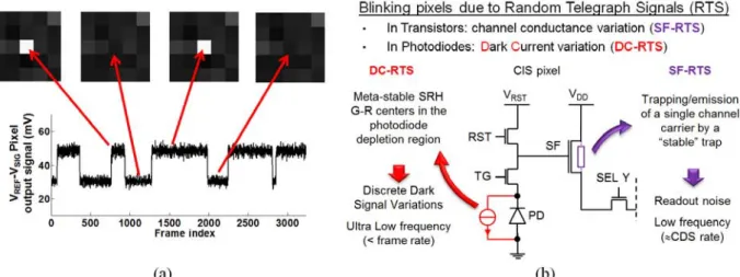
2.2.3 Random telegraph signal noises: DC-RTS and SF-RTS
A Random Telegraph Signal (RTS) is a random process that switches alternatively between two or more discrete levels [76][77] as illustrated in Figure 6a. This phenomenon has been observed in many electronic devices [77] and can have several different physical origins. Several names are used to describe it: RTS, Random Telegraph Noise (RTN), burst noise, popcorn noise, Variable Junction Leakage (VJL)[78] and some application specific names such as blinking pixels in CIS or Variable Retention Time (VRT) in DRAMs[79][80][81]. In CMOS images sensors, RTSs lead to bright pixels that seem to be turned on and off randomly (Figure 6a). Such pixels are generally called blinking pixels. Because of the constant progress in the reduction of dark current and noises, this parasitic behavior is becoming the limiting factor in more and more high-end applications. Two kinds of RTS have been observed in CIS: one due to the discrete fluctuation of the photodetector dark current, called the Dark-Current RTS (DC-RTS) and the other one due to the discrete switching of the in pixel SF MOSFET channel resistance (called the SF-RTS).
6 that decreases when the quasi-neutral region thickness is reduced or when the diffusion length increases (see eq. 7.21
in [58]).
7
As discussed previously, the dark current in a partially-pinned photodiode pixel is lower than the one of a conventional diode pixel simply because the depleted area Aitdep is smaller in the case of the partially-pinned photodiode.
8 If the dark current evolution with temperature is fitted using the Arrhenius law A=K exp(-E
a/kT) [73], the value of Ea
is the activation energy of the dark current.
9 In reality, a slightly higher value than E
g/2 is measured (typically 0.63eV) because of the temperature dependence of
the terms included in the proportionality factor K1.
Figure 6 : Random Telegraph Signal overview: (a) Typical effect of an RTS pixel on dark frames. (b) Summary of the two main RTS phenomena in CIS: Dark Current RTS (DC-RTS) and Source Follower RTS (SF-RTS).
11
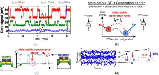
DC-RTS was first reported[82][83][84] and analyzed[85]–[90] in irradiated CCDs and this phenomenon has been attributed to bulk meta-stable SRH generation centers10, located in a depleted region (with p⋅n <ni², such
as a reverse biased PN junction), which are able to instantaneously switch between two generation rates. Since then, this bulk DC-RTS has been observed in CMOS APS[12][91][92], in MAPS[93] and in CIS [94]. It has been recently demonstrated that DC-RTS generation centers can also be located at the depleted Si-oxide interface[95]–[100]. This kind of RTS has the following characteristics:
• the amplitudes of the dark signal discrete fluctuations are proportional to the integration time (as illustrated in Figure 7a) and they can be much higher than what would be expected from a single point defect
• the DC-RTS fluctuations are instantaneous (no transient regime between two states)
• the RTS behavior can directly be observed at the sensor output on the dark signal evolution with time of a single RTS pixel
• the inter-transition times are exponentially distributed and the time constants of DC-RTS are not limited to a particular range (time constants ranging from milliseconds to hours have been reported)
• the maximum transition amplitudes are also exponentially distributed [94][96]
• the time constants and the amplitudes are thermally activated (typically with an activation energy of about 0.6eV for the amplitude in modern CIS)
• one possible explanation for the observed meta-stable generation rate is that DC-RTS is due to a change of configuration of an SRH generation center that has a different generation rate in each configuration (as illustrated in Figure 7b). There is however no clear evidence that these different configurations are linked to the trapping and the emission of charge carriers (contrary to SF-RTS) and the real nature of the DC-RTS centers is not fully understood yet
• the wide majority of DC-RTS pixels observed in unirradiated CIS is coming from meta-stable generation centers located at Si-oxide interfaces (i.e. not from bulk DC-RTS centers)[95], [98]
10 In this manuscript, “meta-stable generation centers” means a generation center (whatever its physical origin: a point
defect, an interface state, a cluster…) that exhibits a generation rate (i.e. a dark current) with two or more metastable states (whatever the physical origin of this apparent signal metastability).
Figure 7 : DC RTS and SF RTS illustrations: (a) One RTS pixel output dark signal versus time (frames) for three different integration durations (tint). (b) Illustration of a possible DC-RTS mechanism. (c) Illustration of the SF RTS physical
mechanism (assuming fixed VG, VD and IDS as in real pixel operation conditions). (d) Effect of SF-RTS on the sensor output
signal: a discrete dark voltage variation is seen only if the source follower RTS state has changed between the two samples (SHS and SHR). Contrary to DC-RTS, SF-RTS meta-stable states are not visible at the sensor output and the SF-RTS amplitude is not proportional to integration time.
12
SF-RTS in CIS is due to the well-known MOSFET gate oxide trapping RTS [101][102]. It is due to the random trapping and emission of inversion channel carriers ([77][103] and references therein). When an electron is trapped by a channel interface state (at the gate oxide or STI oxide interface[103]), the channel conductance is reduced, leading to a low source potential state (as shown in Figure 7c). When the electron is released, the channel conductivity is increased back to its initial value and the MOSFET source voltage is then in a high potential state.
Both phenomena are different physical mechanisms: SF-RTS is a discrete change of channel resistance whereas DC-RTS is a discrete fluctuation of the dark current. They also have different signatures at the CIS output and can thus be easily discriminated. For example, SF-RTS leads to an increase of the sensor temporal noise but the RTS behavior is hardly visible at the output and no stable RTS state can be seen in this case (Figure 7d), contrary to DC-RTS (Figure 7a).
3
Single event effects
As any CMOS IC, APS and CIS are in theory sensitive to all kinds of SEE [16] and this sensitivity strongly depends on the design and the technology of the tested sensor. However, the peripheral circuits of most of the CIS tested in literature do not exhibit high SEE sensitivity (for example, no effect has been observed in [104]) even in extreme conditions such as Inertial Confinement Fusion (ICF) radiation environment[105]. Single Event Latchups (SEL) have been observed in CIS digital circuits [106] whereas simple analog readout circuits are generally immune to SEL (because they usually do not have N and P-MOSFETs close to each other[107]). Single Event Upsets (SEU) have been observed in CIS[108][109] but only in peripheral circuits (such as on-chip sequencers) that embed digital memories, latches or flip-flops. Some Single Event Functional Interrupts (SEFI) [106][110] and some Single Event Transients (SET)[107] have also been reported. Most of these SEE occurring in peripheral circuits can be mitigated by using the classical Radiation-Hardening-By-Design (RHBD) techniques [16], [111]–[114] and SEE in peripheral circuits are not likely to be a problem in radiation hardened CIS.
As most of radiation effects in CIS, the most frequent SEEs occur in the pixel array. Incoming particles generate electron-hole pairs in the sensitive silicon volume through direct (for charged particles) or indirect ionization (for neutrons). These high densities of parasitic carriers are collected like photo-generated signal carriers and they lead to the transient saturation of the collecting pixels. Such pixel SETs can saturate large clusters of pixels [107], [115], [116] or generate secondary recoil ion tracks [105], [117] and several modelling approaches have been proposed in literature to predict their effect on image quality, their occurrence or shape of their track [108], [118]–[120]. The same single particle induced parasitic charge collection mechanisms are also actively studied and modelled in the MAPS community, but in this case, the collected charge is seen as the signal, not as a parasitic SET (see [121] for example). Pixel SETs do not last more than a frame and anti-blooming techniques can help reduce the size of the particle track (in PPD pixels[106] but not in 3T pixels [107]). Anti-crosstalk DTI[43] can also limit the spreading of parasitic charge over several pixels. By thinning the sensor active volume (typically the epitaxial layer in CISs), the effect of SET can be reduced but the signal sensitivity is most often also decreased. In some particular applications, hardening by system techniques can be used to get rid of the unwanted parasitic charge[122], [123]. Other kinds of SEE are not likely in simple 3T or 4T pixels but can be an issue in smart sensors with in-pixel integrated functions.
4
Cumulative radiation effects on peripheral circuits
In most of the cases, radiation effects on peripheral circuits such as address decoders and analog readout circuits are limited to the degradation of the MOSFET characteristics. Thanks to the reduced gate oxide thickness of DSM CMOS technologies, the radiation induced gate oxide degradation is negligible in CIS (even after high levels of TID[124]) and the main MOSFETs degradations come from the radiation induced positive charge trapped in the lateral STI (on the channel edges) [19][125][112]. This remains true despite the fact that
13
CISs use, in the analog parts of the circuit (especially inside the pixel array), “high-voltage”11 MOSFETs (also called I/O or GO2 MOSFETs) with thicker gate oxide (typically 7 nm) than the core “low-voltage” MOSFETs. This trapped charge leads to three main effects in MOSFETs:
• The creation of a parasitic drain to source leakage path on the STI sidewalls (in N-channel MOSFET only)
• A threshold voltage variation in narrow N and P-MOSFETs called Radiation-Induced-Narrow-Channel-Effect (RINCE)[126][127]
• The creation of leakages paths between N doped regions called inter device leakages
For low and moderate TID levels (below 1-10kGy), these effects are generally not a problem in CIS digital and analog circuits outside the pixel array and radiation hardness above 10kGy(SiO2) have been demonstrated
without the use of RHBD techniques[70][99][60]. By using these hardening techniques[112][113][114], such as Enclosed Layout Transistors (ELT), CIS and APS peripheral circuits can even handle TID levels beyond the 100kGy(SiO2) range[8], [10], [13], [128], [129]. Some specific parts of mixed-signal CMOS circuits used in
some CISs may exhibit a lower radiation hardness (and require specific hardening technique), such as sampling nodes (which can suffer from retention time reduction), voltage references or parasitic bipolar transistors[130], [131].
Despite the fact that CIS with integrated sequencers, registers and ADCs have been exposed to ionizing radiation and tested[12], [13], [109], [132]–[138], it has not been demonstrated so far that such peripheral circuits are limiting the TID hardness of CISs. The part of CIS circuits that is the most sensitive to TID is the pixel itself, especially before the charge to voltage conversion (i.e. from the photodetector to the SF MOSFET gate electrode in Figure 2) where any leakage current can impact the sensor performance.
As a surface device, MOSFETs are known to be almost immune to displacement damage effects whereas, as discussed in sec. 5.2, pixels are very sensitive to Dd. Therefore pixel arrays generally become unusable before any displacement damage effect can be observed on the peripheral CMOS circuits.
5
Cumulative radiation effects on pixel performances
5.1
Total ionizing dose effects
5.1.1 Degradation mechanism overview and common effects
In DSM CIS processes, the TID induced degradations of in-pixel MOSFETs are generally secondary[139], [140] compared to the effects on the photodiode (and the associated TGs in PPD pixels). Moreover, in-pixel MOSFETs can be easily radiation hardened by using the RHBD techniques[112][113][114] to extend their radiation hardness much beyond the 10kGy range. This section mainly focuses on the radiation effects on the photodiode (and the TG in PPD pixels).
An overview of the TID induced degradation of three selected pixels is presented in Figure 8. The left column (Figure 8a) represents a PPD pixel with an accumulated TG whereas the center column shows a 4T-PPD pixel with a TG in depletion. The right column shows 3T pixel cross sections. As mentioned in 1.3, ionizing radiation induces the buildup of trapped positive charge in the dielectrics (here the STI and the PMD) and interface states at the Si/oxide interfaces. These defects are distributed all over the dielectrics but only the ones that play a significant role in the radiation induced degradation are represented in Figure 8. Despite the fact that the defect distributions are similar in the three illustrated pixel cross sections, the most limiting defects are not the same in the three pixels. A first look at Figure 8 allows to realize that in the accumulated TG PPD pixel, the most active defects are located on top of the PPD (in the PMD or at its interface) whereas TG channel interface states play the main role at low and moderate TID in a PPD pixel where a TG is in depletion. In a 3T pixel and in any APS pixel based on a conventional or partially pinned photodiode, the most active defects are located on the photodiode perimeter, where the depletion region reaches the oxide.
11 This “high voltage” is typically between 2.5V and 5V, with a popular 3.3V value, which is higher than the operating
14
During TID irradiation, the most degraded parameter in every CIS, APS and MAPS pixel is the dark current (shown in Figure 9a and b). In PPD based pixels with accumulated TG, the dark current starts to rise with TID at low dose because of the interface state buildup at the nearest Si/oxide interfaces[71][72]. In most of the cases, the generating interface is the Si/PMD interface on top of the PPD[72] but in some particular cases12 the main contribution can come from the Si/STI (or Si/DTI) interface[71]. This contribution is an interface state diffusion dark current proportional to the PPD area or perimeter (depending on the dominating oxide) and is described by eq. (4). At higher TID, the Si/PMD interface becomes slightly depleted in the area where it is nearest to the PPD depletion region [72][99][141]. This particular area is the region in the vicinity of the TG sidewall spacer13 as illustrated in Figure 2b and Figure 8a. In this case, the main contribution is an interface state generation dark current (eq. (1)) coming from this depleted interface (that is proportional to the TG width[141]). At even higher TID the PPD depletion region reaches the PMD interface14, the PPD is no more “pinned”, and the interface state generation dark current (eq. (1)) coming from the PMD interface dominates (this contribution is proportional to the PPD area)[99].
12 Such as a very small pixel pitch, a reduced STI-PPD distance, a high P+ pinning doping concentration or a low P
doping concentration between the STI and the PPD.
13 The P doping concentration in the spacer vicinity is lower than the P+ pinning layer doping concentration to reduce
the potential barrier between the PPD and the TG when it is turned ON.
14
and possibly the STI interface too in some extreme cases
Figure 8 : Pixel degradation mechanism illustration in (a) a 4T pinned photodiode pixel with accumulated TG, (b) a 4T pinned photodiode pixel with depleted TG and (c) a 3T pixel with a conventional photodiode. Partially pinned photodiode behave similarly to 3T pixel conventional photodiodes except that some effects may be delayed due to the P+ pinning layer. The low, moderate and high TID levels depend on the manufacturing process but they roughly correspond to the following ranges respectively: below 0.5-1kGy(SiO2), in the 0.5-10kGy(SiO2) range and beyond 1-50kGy(SiO2).
15
In the case of PPD pixels in which a TG is not properly accumulated15, the PPD depletion region reaches the depleted TG channel which is in contact with the gate oxide and channel STI interfaces. The dominant contribution at low and moderate TID becomes the interface state generation dark current (eq. (1)) coming from the gate oxide and TG channel STI sidewalls. It leads to a higher radiation induced dark current increase in depleted TG PPD pixels[62], [72] compared to the one with accumulated TG as shown in Figure 9a. At high TID (3 kGy in Figure 9a), the main contribution comes from the depleted PMD interface and the additional contribution of the depleted TG channel is no more visible.
Other radiation induced dark current sources that are not likely to appear in a PPD pixel with an optimized design manufactured using a mature CIS process have been reported in literature:
• An interface state generation dark current coming from the peripheral STI interface[142] if this interface is in contact with the PPD depletion region16
• Tunneling currents and other high electric field effects (and contamination related dark current issues)[62], [142], [143]
• An unidentified dark current source in[72] that could be explained by an underestimation of the TG contribution17
In 3T pixels (and in any active pixel based on a conventional or partially pinned photodiode) the main source of dark current before and after irradiation is the interface state generation dark current coming from the depleted STI (or PMD in case of partially pinned diode as shown in Figure 2c). In a conventional N-well or N+ -based photodiode, this contribution is proportional to the photodiode perimeter[7], [10], [139], [144]. At low TID the dark current rises with the radiation induced interface state buildup (as expected from (1)). At moderate TID, the STI trapped charge extends the depletion region on the photodiode perimeter leading to a large dark current enhancement (by increasing Aitdep in(1))[8], [13], [145], [146]. At high TID, the field oxide interface
(STI or DTI) is inverted, the photodiodes are shorted, the CVF drops and the pixel array is no longer functional (see [70] for example). The same degradation mechanism appears in partially pinned photodiodes except that the depleted interface area is smaller before irradiation than in a conventional diode and except that the effects might be delayed to higher TID if the pinning implant concentration is much higher than the one at the bottom of the STI in a conventional diode.
In all the pixel types, this TID induced dark current is pretty uniform as illustrated by the nice Gaussian distribution (from [147]) shown in Figure 9b which leads to a uniform increase of the grey level in the dark frame.
The EQE is also degraded by ionizing radiation. The radiation induced interface states (blue crosses in Figure 9c) act as recombination centers for the excess minority carriers generated by the incoming light. The signal carriers generated close to the interfaces are lost by recombination at this interface leading to a decrease of EQE for the shortest wavelengths in FSI devices[140], [142] (as shown in Figure 9d). In the case of a BSI sensor, a Si-oxide interface exists on both CIS sides (front and back sides). Therefore, the EQE drop may appear at both short and long wavelengths as illustrated in Figure 9d. For the same reasons, charge collection efficiency also drops in TID irradiated MAPS[148]. As regards the effect of ionizing radiation on the optical properties of the dielectric stack (ILDs, passivation and buffer layers, microlenses…) no clear evidence of degradation has been reported in APS/CIS and it seems that up to 3kGy(SiO2) microlenses properties are not degraded [140].
Similar conclusions have been drawn on the radiation hardness of color filters (but in a more limited TID range[149]).
15 This is generally the case for the second TG used for AB of GS operation in a 5T-PPD-pixel such as the one tested
in[138]. It also happens in 4T-PPD-pixel where a positive voltage is applied on the TG to use the FD as an AB drain.
16
It should not happen if the PPD-STI distance is sufficient and if the P-doping concentration between the PPD and the STI is sufficiently high.
17 In the light of recent conclusions on the effect of the EFWC concept on dark current non-linearities[141], it seems
possible that the more intense dark current contributions (the TG related ones) have been underestimated in [72]. Since I0 is
determined in [72] by subtracting all the other contributions (PPD area, PPD perimeter, TG channel…) to the measured dark current, the reason why I0 is not null could be a consequence of such underestimation.
16
Ionizing radiation also enhances the noise sources. The SF contribution increases18 with TID[71][151] and generally dominates at low TID19 but the dark current shot noise contribution (that rises as the square root of the dark signal) can quickly become the dominant temporal noise20 source at higher dose (as illustrated in Figure 10a). Comparable noise degradation mechanisms are observed in MAPSs[146], but the dominant radiation induced noise sources may be different because MAPS readout circuit architectures differs generally from classical CIS ones (this can also be true in “smart-pixel” CISs). In PPD CISs, the charge transfer noise[153], [154] can start to have a visible contribution at moderate or high TID[71] when the CTE is strongly degraded (as discussed in the next section).
The number of RTS pixels rises as well with the absorbed ionizing radiation dose as illustrated in Figure 10b. Contrary to what was observed in the first DC-RTS studies[85], [86], [92], TID creates DC-RTS centers21 very effectively in DSM CIS[95], and nearly 100% of 3T-CIS pixels can exhibit an oxide DC-RTS behavior after a TID as low as 100 Gy [96] because of the interface state buildup on the photodiode depleted perimeter (same origin as the mean dark current increase). As discussed in section 2.2.3, the amplitude of DC-RTS are exponentially distributed (with an average RTS maximum amplitude in the 100 e-/s range at 22°C and with extreme values up to several ke-/s [95], [96]). This type of oxide RTS is mainly bi-level and most of more-than-two-level TID induced RTS seem to be due to the superimposition of two or more oxide interface DC-RTS
18 as in any irradiated MOSFET (see for example [150])
19 The SF contribution can be reduced by using a buried channel SF MOSFET[152]. 20 depending on the integration time and the CVF value
21
i.e. meta-stable generation centers located at the Si-oxide interface
Figure 9 : Common TID induced degradations: (a) Typical mean dark current increase measured on a 7µm pitch 4T-PPD-CIS (modified from [141]). (b) Typical dark current distribution evolution with TID measured on a 10 µm pitch 3T image sensor (modified from [147]). Both sensors were exposed to 60Co gamma-rays. (c) Localization of TID induced interface
17
centers22. TID induced oxide DC-RTS can be significantly reduced in 3T CIS pixels by recessing the STI from the photodiode depletion region[95], [96].
In PPD pixels with properly accumulated TGs (main TG and secondary AB/GS TG), the pinning layer protects the diode from the DC-RTS centers at the Si-oxide interfaces and there is almost no DC-RTS in unirradiated CIS[98] and in those exposed to low TID (below the kGy range)[99]. At higher TID, the depletion of the oxide interface in the spacer vicinity (illustrated in Figure 8a, at moderate TID) leads to a steep increase of the number of DC-RTS pixels and most of the pixel array suffers from oxide RTS when the absorbed TID approaches the kGy range[99] (despite the TG accumulation). If at least one of the TGs is not accumulated, oxide DC-RTS pixels exist before irradiation[98] and their number starts to rise significantly at a much lower TID than in the accumulated TG case [99], [100] because the PPD is not protected from the DC-RTS centers located at the TG channel oxide interfaces [98], [99]. With a non-accumulated TG, a PPD CIS can be saturated by oxide DC-RTS pixels well below the kGy range (as in 3T-pixel).
Since SF-RTS is linked to the presence of interface states in the MOSFET channel (at the gate-oxide or STI interface), ionizing radiation should have a strong influence on the number of pixels exhibiting SF-RTS. The few results that can be found on TID induced SF-RTS in literature show that the SF-RTS pixel creation is hardly noticeable even after 10-20 kGy of TID (no increase observed in [155] and less than 0.3% of SF-RTS pixels created by the radiation exposure in [151]). The very good radiation hardness of DSM-MOSFET gate oxides could explain why very few SF-RTS are created by TID but the reason why SF-RTS coming from the SF channel STI is not visible is still unclear.
5.1.2 Pinned photodiode specific effects
In addition to the cumulative ionizing radiation effects common to all type of APS/CIS, some specific radiation induced degradations have been observed in PPD based CISs. The first effect is a right shift of the Vpin
characteristic, illustrated in Figure 11a, caused by the PMD positive trapped charge[99], [141] (represented by the plus sign in the PMD in Figure 8a) that acts as a positively biased CCD gate on top of the PPD. This left shift indicates an increase of pinning voltage and EFWC. At high TID (above ≈ 10 kGy(SiO2)), the pinning
layer effective doping is largely reduced by the PMD positive trapped charge, leading to a PPD capacitance decrease (visible on the Vpin curve as a slope diminution) and eventually to the complete depletion of the
Si/PMD interface on top of the PPD (as shown in Figure 8a)[99][156]. Despite a large degradation of the PPD structure in the kGy(SiO2) range, the charge partition step (at Vstep) linked to the TG threshold voltage is not
shifted, indicating that the TG threshold voltage is not affected at this TID level. A subthreshold leakage may however appear on the characteristic at moderate/high TID as presented in Figure 11a.
22 However, some complex multi-level oxide RTS that can not be explained by the simple sum of independent
DC-RTS center contributions have also been reported[95], [98].
Figure 10 : Radiation effects on CIS noises. (a) Typical evolution with TID of the main temporal noise contributions. This illustration represents a possible dark current shot noise increase assuming a linear dark current evolution with TID. (b) Typical evolution with TID of the number of pixels exhibiting DC-RTS or SF-RTS behaviors. The range at which nearly 100% of the pixel population exhibit DC-RTS can be below 100 Gy for 3T pixels and in the kGy range for PPD pixels.
18
As regards the transfer efficiency, several mechanisms can limit the CTE in a CIS: the existence of a potential barrier or pocket in the transition region from the PPD to the TG[157] or a high density of interface states in the channel that can trap the signal carriers[158]. The TID induced surface potential increase caused by the PMD positive trapped charge has an influence on the CTE (illustrated in Figure 11b and c). The most sensitive part of the pixel for the transfer is right below the TG sidewall spacer because the N doped PPD region comes closer to the interface (partly because the surface P doping concentration is lower than in the rest of the pinning layer) to ensure a good CTE. In this region, the PMD/spacer positive trapped charge has a much stronger influence on the PPD channel than in the rest of the PPD. In “low lag” pixels (i.e. with no limiting potential barrier or pocket before irradiation), this local potential augmentation creates a potential pocket that degrades the CTE (case A in Figure 11b and c). In PPD pixels limited by a potential barrier before irradiation, the exposure to ionizing radiation reduces the potential barrier and leads to a CTE improvement at low TID (case B in Figure 11b and c). At high TID, the potential pocket expansion outweighs the benefit of the potential barrier lowering and the CTE is degraded with TID as in case A.
The last PPD specific effect concerns the FWC variations23. We have just discussed that the PMD trapped charge increases the EFWC. Since all the FWC definitions are linked to the EFWC (as mentioned in 2.2.1 and as can be seen in Figure 4c and Figure 11d), it should lead to an increase of both the FWCΦ and the FWCdark. In
practice, other mechanisms are competing with the EFWC growth as depicted in Figure 11d. The first one is the increase of TG subthreshold current[143] (mainly due to the TID induced parasitic STI sidewall channel
23 Some saturation voltage variations with TID can be observed in 3T pixels, but they are linked to the readout circuit
(e.g. the reset MOSFET in soft reset mode in [140]), not to the photodiode physical FWC.
Figure 11 : Pinned photodiode specific radiation effects. (a) Evolution of the pinning voltage characteristic with TID. (b) Charge Transfer Inefficiency (CTI=1-CTE) evolutions with TID of a barrier limited pixel and a low lag pixel. (c) Illustration of the CTE degradation mechanism (modified from [141]). (d) Illustration of the FWC degradation mechanism. (e) Measured relative FWC degradations on a 7 µm-pitch 4T-PPD CIS (data from [141]).
19
pictured in Figure 8.a and b) that can be represented as a left shift of the dashed red Isubth curve in Figure 11d. It
leads to a left shift of the intersections between the Isubth curve and the other photodiode current curves. Since
these intersections define the FWC values (as discussed in 2.2.1), it means that the TG Isubth reinforcement
causes a reduction of the FWCΦ and FWCdark values that can compensate some of the EFWC augmentation. It is
the main reason why the relative FWCdark increase in Figure 11e is weaker than the EFWC growth.
The second phenomenon is the dark current enhancement with TID that leads to a much steeper slope24 of the reverse current exponential I-V characteristics (Idark and Iphot+Idark) near IPPD = 0. Because of this steeper
slope, the FWCΦintersection is shifted toward the EFWC point (as depicted in Figure 4d). Since in most of the
cases the FWCΦ is greater than the EFWC, it means that the large dark current rise with TID leads to an
important reduction of the FWCΦ that can be larger than the EFWC increase and thus to an overall decrease of
FWCΦ with TID. This mechanism seems to be the main cause of the FWCΦdrop with TID shown in Figure 11e
and the subthreshold current contribution appears to be secondary in the few experimental conditions (technology, design and operating conditions) tested in literature[141]. All these graphical interpretations are supported by the analytical model developed in[63], [64], and the same conclusions can be drawn by using directly these equations.
5.1.3 Radiation-hardening of CIS pixels
As mentioned previously, in-pixel MOSFETs (all except the TG) can be radiation hardened by using classical RHBD techniques. Unfortunately, RHBD for CMOS ICs cannot be used to mitigate the TID effects presented in this section and dedicated techniques have to be used. In APS and CIS based on conventional photodiodes (e.g. 3T pixels), the main issue is the depletion region extension on the photodiode perimeter and the buildup of interface states along this depleted interface. Several techniques have been proposed in literature[7], [9], [10], [70], [139], [144], [159]–[161] and all of them are based on the recess of the isolation oxide to control the potential on the photodiode perimeter by using P+ implants or a polysilicon gate. One possible solution is the gated photodiode layout that is presented in Figure 12a in which a polysilicon gate is accumulated to control the potential on the photodiode perimeter. This kind of solution generally brings a higher dark current before irradiation but delays the dark current increase with TID and prevents the loss of pixel functionality that can happen if the isolation oxide becomes inverted.
According to the degradation mechanisms presented in Figure 8, the main issues in PPD pixels come from the positive trapped charge in the PMD (including the TG spacer) and from the Si/PMD interface. These two degradation sources could possibly be mitigated by placing an electrode on top of the PPD (Figure 12b and c) to prevent or compensate the positive charge trapping in the PMD as proposed in [141]. Using an enclosed layout TG has also been proposed to improve the radiation hardness of PPD CIS [162], [163]. This latter solution prevents the creation of the parasitic TG subthreshold leakage path and it should also reduce the TID induced FD leakage. Unfortunately, this solution is inefficient[141] against the main degradation source discussed here: the PMD/spacer trapped charge.
24
i.e. a higher first derivative absolute value of the photocurrent (IFW in [63]) near the X-intersect point.
Figure 12 : Photodiode Radiation-Hardening-by-Design technique examples. (a) One of the several proven solutions for conventional photodiodes: the gated photodiode layout [10]. (b) A recently proposed solution for BSI PPD CIS [141] the use of a DC biased polysilicon gate on top of the PPD to mitigate the PMD trapped charge. (c) Same solution but with a metallic gate instead of the polysilicon gate.
20
Some radiation-hardening-by-process techniques have also been reported in literature to improve the radiation hardness of 3T pixels [144] such as the use of a custom surface P+ pinning implant[13] (leading to a partially pinned photodiode structure) but, these custom process steps may not be available in the targeted manufacturing process. For PPD CIS, the hole based PPD[158], [164], [165] (also called PMOS PPD or P-channel PPD) seems to be a promising radiation-hardening-by-process solution but very few data have been published[164] on this technology behavior when exposed to ionizing radiation.
5.2
Displacement damage effects
5.2.1 Overview
Non-ionizing interactions create SRH centers (point defects or cluster of defects) in the silicon bulk [24]. In APS and CIS, these defects are mainly active in the photodiode vicinity as pictured in Figure 13a. They act as SRH generation centers in depleted regions leading to a growth of the bulk generation dark current (eq. (2) and (3)) discussed more in detail hereafter. These defects also act as recombination centers that reduce the recombination lifetime of photogenerated minority carriers [166][167]. When signal electrons are generated near the collecting depletion region, they have very little chance to recombine before being collected. On the other hand, electrons generated far from the PN junction must diffuse over a large distance before reaching the collecting well. Therefore, in FSI CIS, displacement damage mainly impacts the EQE at long wavelengths whereas in the case of BSI CIS all the wavelengths can suffer from an EQE reduction due to displacement damage (with a higher effect at short wavelengths) as illustrated in Figure 13b. Indeed, in BSI devices, the majority of signal carriers are generated near the back interface (whatever the photon wavelength) far from the depletion region. Carrier lifetime reduction is expected for displacement damage dose beyond 40 TeV/g (≈ 2×1010 cm-2 1 MeV neutron equivalent fluence and more than 1×1010 cm-2 of 50 MeV protons [167]). However such effect is rarely reported in CIS, even after several PeV/g of absorbed dose, because the effective recombination lifetime is generally limited by the surface recombination or by the thin thickness of image sensors optimized for visible wavelengths (typically a few microns). On the other hand, charge collection efficiency drops are typically observed on MAPSs after 200 TeV/g (1×1011 cm-2 1 MeV equivalent fluence) [9], [121], [168], [169] because their sensitive layer is often thicker than in CISs. At even higher Dd, change of effective doping concentration may occur (as suggested in [170] to justify the FWC reduction25) because of carrier removal or type inversion[171], but the particle fluence necessary to see these effects on APS/CIS are rarely reached.
Finally, these SRH centers can also act as bulk traps able to capture a signal carrier and to release it later. But contrary to CCDs[58], Dd induced CTE degradation due to bulk trapping in CIS has never been reported. This is mainly due to the limited number of charge transfers necessary to read the signal charge (none in 3T pixels and one in PPD CISs) compared to CCDs. Capture and delayed emission could possibly occur in the quasi-neutral silicon bulk, far from the junction, but such phenomena are not likely to appear in classical slowly varying illumination conditions used to characterize CISs.
5.2.2 Dark current, DCNU and RTS
As for TID, the main Dd effect is the dark current augmentation. Figure 13c shows a typical dark current distribution after exposure to non-ionizing radiation. Unlike TID, Dd leads to strong non-uniformities that appear as a hot pixel tail26. For a given dose (and for NIEL > 10-4 MeV cm²/g), the mean dark current increase induced by non-ionizing radiation in a depleted silicon volume Vdep can be determined by using the Srour
Universal Damage Factor (UDF)[172]:
d dep dark dark K V D I = × × ∆ (6)
The validity of this equation has been verified several times in modern CISs (as illustrated in Figure 13d) where the optimized manufacturing process limits the high electric field regions[94], [138], [140], [173], [174].
25 However, this FWC reduction could be due to the dark current increase, as discussed in section 5.1.2.
26 It is interesting to notice in Figure 13c that charged particle irradiation (such as protons) leads to both TID and D
d
![Figure 4 : Illustrations of the different Full Well Capacity definitions in PPD CIS. (a) Measurement of the different FWC on a PPD CIS (modified from [64])](https://thumb-eu.123doks.com/thumbv2/123doknet/3226804.92323/9.892.96.797.166.394/figure-illustrations-different-capacity-definitions-measurement-different-modified.webp)


![Figure 9 : Common TID induced degradations: (a) Typical mean dark current increase measured on a 7µm pitch 4T-PPD- 4T-PPD-CIS (modified from [141])](https://thumb-eu.123doks.com/thumbv2/123doknet/3226804.92323/17.892.124.771.163.636/figure-common-degradations-typical-current-increase-measured-modified.webp)


