Radiation Effects in Pinned Photodiode CMOS Image Sensors: Pixel Performance Degradation Due to Total Ionizing Dose
11
0
0
Texte intégral
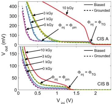
Figure
+4
Documents relatifs