HAL Id: hal-00799899
https://hal.archives-ouvertes.fr/hal-00799899
Submitted on 12 Mar 2013HAL is a multi-disciplinary open access archive for the deposit and dissemination of sci-entific research documents, whether they are pub-lished or not. The documents may come from teaching and research institutions in France or abroad, or from public or private research centers.
L’archive ouverte pluridisciplinaire HAL, est destinée au dépôt et à la diffusion de documents scientifiques de niveau recherche, publiés ou non, émanant des établissements d’enseignement et de recherche français ou étrangers, des laboratoires publics ou privés.
Mechanical Study of Copper Bonded at Low
Temperature Using Spark Plasma Sintering Process
Bassem Mouawad, Maher Soueidan, D. Fabregue, Cyril Buttay, Vincent Bley,
Bruno Allard
To cite this version:
Bassem Mouawad, Maher Soueidan, D. Fabregue, Cyril Buttay, Vincent Bley, et al.. Me-chanical Study of Copper Bonded at Low Temperature Using Spark Plasma Sintering Pro-cess. Advanced Materials Research, Trans Tech Publications, 2011, 324, pp.177-180. �10.4028/www.scientific.net/AMR.324.177�. �hal-00799899�
Mechanical Study of Copper Bonded at Low Temperature
using Spark Plasma Sintering Process
Bassem Mouawad
1, a, Maher Soueidan
1, 2, b, Damien Fabrègue
3, cCyril Buttay
1, d, Vincent Bley
4, eand Bruno Allard
1, f1 Université de Lyon, INSA de Lyon, AMPERE-UMR 5005, Bât. L. de Vinci, 21, Av. J. Capelle,
69621 Villeurbanne Cedex – France.
2 Lebanese Atomic Energy Commission, P.O. Box 11-8281, Riad El Solh 1107 2260 Beirut,
Lebanon
3 Université de Lyon, INSA de Lyon, MATEIS-UMR 5510, Bât. B.PASCAL, 25 avenue J. Capelle,
F-69621 Villeurbanne Cedex, France.
4 LAPLACE Laboratory, Paul Sabatier University, INPT, CNRS, 31062 Toulouse cedex 9 France a[email protected], b[email protected], c[email protected],
d[email protected], e[email protected], f[email protected]
Keywords: Copper bonding, Spark Plasma Sintering, Tensile test
Abstract. Bonding of high purity polished copper was investigated using the Spark Plasma Sintering technique (SPS) showing the effect of SPS parameters (surface roughness, time, temperature and pressure) on the bonding strength behaviour. Mechanical characterization of the bonded samples was performed at room temperature using tensile test. Two surfaces roughnesses were studied (un-polished and polished samples). It was found that the bonding strength varied from 50 MPa to 233 MPa for un-polished and polished surfaces respectively The tensile strength of the used bulk copper-rod was found to be 365 MPa, while most results are over 122 MPa (a third of the bulk value).
Introduction
The work presented here is aimed at developing a new interconnect technology for power electronic devices. Such new technology must provide a very low electrical and thermal resistance. Furthermore, the manufacturing conditions must be compatible with the semiconductor dies (temperature, pressure) and with the industrial constraints (time). Therefore, we present here a technique in which pieces of copper are joined together at temperature lower than 300 °C, with a short turnaround cycle (30 min max) and a relatively low pressure (16-77 MPa).
Several experiments on Cu/Cu direct bonding have been reported [1-3]. Although the methods are simple, they require either high external pressure and annealing or toxic chemical cleaning processes to achieve a reasonable bonding strength. For example, Cu wafers exhibit good bonding properties when Cu/Cu contacts are carried out at 400 °C and 4 bar for 30 min, followed by an annealing cure at 400 °C for 30 min in N2 atmosphere [4]. Another solution, the so-called Surface
Activated Bonding (SAB) process was used to bond Cu-coated wafers at room temperature without any wet chemical process. SAB is a process that joins similar or dissimilar materials by means of the adhesion force between atoms of two atomically clean surfaces in an ultrahigh vacuum UHV at room temperature [5,6]. The same authors also reported that the bonding strength of Cu/Cu interface is approximatively 6.47 MPa [7]. J. W. Elmer & al [8] have presented a diffusion bonding of high purity copper using a conventional furnace. A series of diffusion bonds was done to determine the relationship between bond strength and bonding parameters in order to determine a range of bonding conditions. Bonding strengths of 65 MPa and 190 MPa were found using uniaxial tensile testing for samples bonded at 400 and 800°C respectively (bonding time 60 min).
In general, high temperature annealing (>400°C) is required to increase the bonding strength. However, semiconductor devices have been designed to meet the requirement of the existing soldering technology (a few seconds above 300°C). Therefore, an increase in the process temperature could require heavy modification in the dies manufacturing parameters to avoid possible degradation. In this paper, we report the Cu/Cu direct bonding using Spark Plasma Sintering (SPS) where we focus on the bonding issue by evaluating the bonding strength as a
function of temperature, surface roughness, pressure and bonding time.
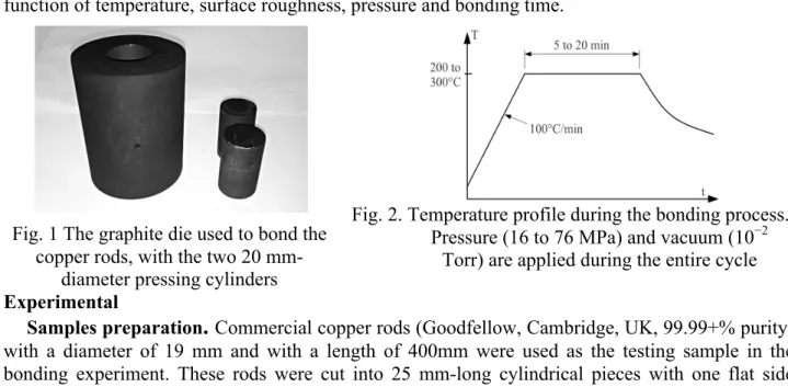
Fig. 1 The graphite die used to bond the copper rods, with the two 20
mm-diameter pressing cylinders
Fig. 2. Temperature profile during the bonding process. Pressure (16 to 76 MPa) and vacuum (10!2
Torr) are applied during the entire cycle
Experimental
Samples preparation
.
Commercial copper rods (Goodfellow, Cambridge, UK, 99.99+% purity) with a diameter of 19 mm and with a length of 400mm were used as the testing sample in the bonding experiment. These rods were cut into 25 mm-long cylindrical pieces with one flat side manually polished. The polishing procedure starts with 220- grit silicon carbide, down to 3 "m diamond paste and 0.05 "m of silica.The samples were then cleaned as follows (i) ultrasonic cleaning in acetone to remove the lubricant, (ii) ultrasonic cleaning in trichloroethylene, (iii) ultrasonic cleaning in microelectronic grade ethanol, (iv) the samples were immersed in 5% HF for 1 min at room temperature for oxide elimination (v) followed by rinsing in DI water and blow drying with nitrogen gas.
Bonding Process. The Cu/Cu bonding was carried out with a Spark Plasma Sintering (SPS) system (FCT HPD 25). As with a classical sintering press, a SPS system applies both pressure and heat to the samples. The difference is that the heat is provided by a pulsed DC-current circulating through the graphite die (or through the sample if it is conductive), whereas the conventional sintering press uses external heating elements. As a result in the case of the SPS, the heat is generated much closer to the sample, offering very fast temperature dynamics: more than 100 K/min for the system used in this study, using current pulses of several kA.
In each experiment, two copper pieces were introduced in a graphite die of 20 mm inner diameter (Fig. 1). The bonding was performed in vacuum (10!2 torr). Temperature, pressure and dwell time were set according to Fig. 2. The temperature was measured using a thermocouple through a hole in the graphite die, as shown in Fig.1. The heating rate was fixed to 100 K/min and the holding time was varied from 5 to 20 minutes (Fig. 2).
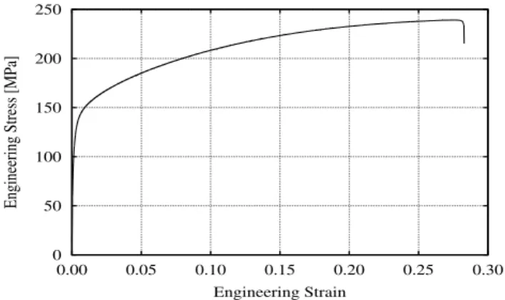
Characterization. After bonding the samples were machined for the mechanical test (tensile test), as described in Fig. 3. Mechanical testing of the bonded samples was performed at room temperature using a MTS Adamel Lhomargy-DY35 with a 20kN cell force. The displacement rate was set up to 1mm/min. Copper being ductile, the sample quickly enters plastic deformation during the tensile test (Fig. 4). This results in a reduction of the actual section of the sample as it elongates. In this document, a nominal stress value is calculated using the initial surface of the tensile sample. It will thus constitute a lower bound of the true stress experimented on the sample. It should be mentioned that all the samples fractured along the bond line (due to the design of the sample). Surface microstructure observations were studied by a Leitz optical microscope and a scanning electron microscope (SEM Philips XL20).
Results and discussion
Surface roughness. A series of Cu/Cu bonding was made to determine the relationship between bond strength and bonding parameters such as bonding temperature, holding pressure and dwell time, in order to determine a range of bonding conditions that could be used to produce satisfactory joints.
Fig. 3 Shape (a) and photograph (b) of the
samples used for the tensile test Fig. 4 Tensile test result for one of the sample (sample 2 in table 1)
For this purpose, two polished rods were bonded at 300°C for 20 minutes and a pressure of 16 MPa. The same conditions were used to bond together two un-polished rods. Both experiments resulted in a proper bond. On both assemblies, the bonding interface was not visible, obviously leading to the conclusion that SPS process has enabled to create a Cu/Cu joint with this set of parameters. Tensile tests, however, revealed two different behaviours for the polished and un-polished samples. In the case of un-un-polished sample, fracture occured without significant plasticity, and at a relatively low maximal force (50 MPa). For the polished sample, fracture occured after a lot of plastic deformation, exhibits a large ductility, and a high maximum force (233 MPa).
Temperature, time, pressure. Table 1 summarizes a list of the experiments, with the corresponding tensile strengths. All these experiments were performed with polished samples for different temperature, holding pressure and dwell time. The first eight experiments show a variation of time (5 and 20 min), holding pressure (16 and 77 MPa, which correspond to the pressure applied on a 20mm-diameter sample) and the bonding temperature (200 to 300 °C). Fig. 5 shows the influence of different parameters on the bonding strength.
The couples (t,T), (t,P), (T,P) and (t,T,P) express the conjugated effect of time, temperature and pressure between each other and they are given a normalized values (-1,1). It can be seen that time and pressure has the expected effect: an increasing in either of these parameters results in a stronger bond.The negligible influence of temperature and the negative effect of the simultaneous increase of time and temperature can firstly be surprising, but can actually be explained by the following considerations: in these tests, a good bond could be achieved for any temperature or time value. However, the application of temperature to the samples also constitutes a heat treatment of the copper. The effect of such treatment on work-hardened copper is a change in its microstructure. For example, increasing the temperature from 200 °C to 300 °C would involve further annealing recovery and recrystallization of the sample, decreasing its overall mechanical properties.
Fig. 5 Influence of different parameters on engineering stress
Moreover, 5 experiments have been assembled with the same experimental parameter (at 250 °C) in order to characterize the reproducibility and accuracy of the bonding process and of the tensile tests. From these measurements, an average tensile strength value of 164.4±20% was calculated. This fairly large tolerance is due to the low sample count, as well as to the low reproducibility of the tensile tests: a much bigger number of samples is usually required but this was unpractical in our case.
0 50 100 150 200 250 0.00 0.05 0.10 0.15 0.20 0.25 0.30
Engineering Stress [MPa]
Engineering Strain
Table 1 Strength bonding and hardness as function of time and temperature for SPS copper bonding with polished surface Sample Time [min] Temperature [°C] Pressure [MPa] Engineering stress [MPa] 1 5 300 77 181 2 20 300 77 239 3 20 300 16 170 4 5 300 16 132 5 5 200 77 106 6 20 200 77 270 7 20 200 16 261 8 5 200 16 No bond (0) 9 20 250 16 150 10 20 250 16 141 11 20 250 16 180 12 20 250 16 169 13 20 250 16 183
Fig. 6 SEM image of the fracture surface (after tensile test), for a sample bonded at 300 °C for 20 minutes and with a pressure
of 16 MPa)
Even with the limited variation range for all three factors (5-20 minutes, 200–300 °C, and 16–77 MPa), substantial differences were found in tensile strength. In most cases, however, a very good bond was formed: the tensile strength of the used bulk copper-rod was found to be 365 MPa, while most results in table 1 are over 122 MPa (a third of the bulk value).
Another evidence of the good bond quality is visible in Fig. 6: the fracture surface is characteristic of ductile fracture with the presence of dimples. This means that the sample has been heavily deformed, which is also exhibited by the large strain value attained during the tensile tests (as can be seen for example in figure 4). Similar patterns were found over the entire fracture surface and for all samples.
Summary
The high purity copper-to-copper bonding technique using SPS is presented. The un-polished sample showed considerably less bonding strength than the polished sample. A bonding strength higher than previously reported in the literature was found (between a third and more than two thirds of the bulk copper tensile strength). This bond is compatible with the requirements of the application: a semiconductor die can sustain temperatures up to 300 °C for a few minutes and pressures in the order of a few tens of MPa.
References
[1] A. Fan, A. Rahman, R. Reif, Copper Wafer Bonding, Electroch. S-S Let. 2 (1999) 534-536. [2] K. N. Chen, A. Fan, R. Reif, Copper Bonded Layers Analysis and Effects of Copper Surface
Conditions on Bonding Quality for Three-Dimensional Integration, J. Elec. Mat. 34 (2005)
1464-67.
[3] Y. A. Li, R. W. Bower, I. Bencuya, Low Temperature Copper to Copper Direct Bonding, J.J. App. Phy. 37 (1998) 1068-69.
[4] K. N. Chen, A. Fan, R. Reif, Microstruture Examination of Copper Wafer Bonding, J. Elec. Mat. 30 (2001) 331-335.
[5] H. Takagi, K. Kikuchi, T. R. Chung, T. Suga, Surface activated bonding of silicon wafers at room temperature, App. Phy. Let. 68 (1996) 2222-4.
[6] H. Takagi, R. Maeda, T. R. N. Hosoda, T. Suga, Room-Temperature Bonding of Si Wafers to Pt Films on SiO2 or LiNbO3 Substrates Using Ar-Beam Surface Activation, J.J. App. Phy. 38
(1999) 1559-61
[7] T. H. Kim, M. M. R. Howlader, T. Itoh, T. Suga, Room temperature Cu–Cu direct bonding
using surface activated bonding method, J. Vac. Sci & Technol A 21 (2003) 449-453.
[8] J. W. Elmer, J. Klingmann, and K. Van Bibber, Diffusion bonding and brazing of high purity copper for linear collider accelerator structures, Phys. Rev. ST-Acc. Beams 4 (2001) 53502-1-16.
![Table 1 Strength bonding and hardness as function of time and temperature for SPS copper bonding with polished surface Sample Time [min] Temperature[°C] Pressure [MPa] Engineering stress [MPa] 1 5 300 77 181 2 20 300 77 239 3 20 300](https://thumb-eu.123doks.com/thumbv2/123doknet/14324290.497558/5.892.80.807.103.409/strength-hardness-function-temperature-polished-temperature-pressure-engineering.webp)
