Design of a Continuous-Time Bandpass
Delta-Sigma Modulator
by
Xi Yang
Submitted to the Department of Electrical Engineering and Computer
Science
in partial fulfillment of the requirements for the degree of
Master of Science in Electrical Engineering
at the
MASSACHUSETTS INSTITUTE OF TECHNOLOGY
ARCHNE$
MA(SSACHUSETTS INSTiifCE i OF TECHNOLOGYAPR
1
0
201
LIBRARIES
February 2014
©
Massachusetts Institute of Technology 2014. All rights reserved.
A u th o r ...
.
... .. ...
Department of Electrical Engineering and Computer Science
January 7, 2014
Certified by...Hae-Seung Lee
Professor
Thesis Supervisor
Accepted by.
L)Leslie A. Kolodziejski
Design of a Continuous-Time Bandpass Delta-Sigma
Modulator
by
Xi Yang
Submitted to the Department of Electrical Engineering and Computer Science on January 7, 2014, in partial fulfillment of the
requirements for the degree of Master of Science in Electrical Engineering
Abstract
An 8th-order continuous-time (CT) bandpass delta-sigma
(AZ)
modulator has been designed and simulated in a 65 nm CMOS process. This modulator achieves in simulation 25 MHz signal bandwidth at 250 MHz center frequency with a signal-to-noise ratio (SNR) of 75.5 dB. The modulator samples at 1 GS/s while consuming319 mW. On the system level, the feedback topology secures stability for the 8th-order
system, achieving a maximinn stable input range of -1.9 dBFS. A 2.5-V/1.2-V dual-supply loop filter with a feed-forward coupling path has been proposed to suppress noise and distortion. On the transistor level, a 5th -order dual-supply feed-forward
operational amplifier (op amp) and a 4th-order single-supply feed-forward op amp
have been designed to enable high modulator linearity and coefficient accuracy.
Thesis Supervisor: Hae-Seiing Lee
Acknowledgments
First and foremost, I would like to express my sincere gratitude to my advisor, Prof. Hae-Seung Lee. It has been a tremendous privilege to work with him. I have always been inspired by his insight and intuition in analog circuit design. His guidance have allowed me to complete this thesis successfully.
In addition, I would like to heartily thank my colleagues who are all brilliant, sincere, and always willing to help. I have learned so many things from them and have always admired their talent, creative work, and conscientious attitude towards research. I would like to thank especially Do Yeon, Sunghyuk, and Kailiang for their generous help and valuable advice, and Daniel, Sabino, Sungwon, and Joohyun for
their encouragements and helpful discussions.
I shall extend my thanks to Stacy Ho from MediaTek, who supervised me during
my internship in the sunner of 2012. He helped me gain a better understanding of continuous-time delta-sigma modulators, and showed me what it takes to be a good analog designer.
I shall also show my gratitude to Prof. Alex Lee, my undergrad advisor. He
opened the door to the analog world for me and offered me enormous help in my grad school applications. I could not have got the chance to study here at MIT if it were not for his support.
I would like to thank mriy friends, especially Qiannan, Xueting, Xiaoxing, Chen,
and Yixiao for always being there and believing in me.
Last but most importantly, I would like to express my deepest gratitude to my parents and my grandmother for their enduring love, support, and faith in me. I could never have completed my journey this far without their care, encouragements, and understanding.
Contents
1 Introduction 17
1.1 M otivation . . . . .. . . . 17
1.2 Previous W ork . .. . . . 19
1.3 Thesis Organization. . . . . 21
2 Delta-Sigma Modulator Basics 23 2.1 Analog-to-Digital Conversion . . . . 24
2.2 Delta-Sigma Modulation . . . . 27
2.2.1 Oversampling . . . . 27
2.2.2 Noise-Shaping . . . . 29
2.2.3 Bandpass Delta-Sigma Modulation . . . . 32
2.3 Modulator Implementation . . . . 33
2.3.1 Discrete-time Delta-Sigma Modulator . . . . 33
2.3.2 Continuous-time Delta-Sigma Modulator . . . . 34
2.3.3 Impulse Response Matching . . . . 36
2.4 Summary . .. . . ... . . . .. .. .. . . 37
3 Modulator Architecture 39 3.1 Desired Modulator Specifications . . . . 40
3.2 NTF Selection . . . ..41
3.3 Realizing Complex NTF Zeros . . . . 43
3.4 Modulator Topology . . . . 43
3.4.2 Modified Feedback Topology . . . .. 47
3.5 Determining Coefficients . . . .. 48
3.5.1 Determining Coefficients . . . .. 48
3.5.2 Coefficient Scaling . . . . 49
3.6 Sum m ary . . . . 49
4 Loop Filter Implementation 51 4.1 Loop Filter . . . ..52
4.1.1 Op Amp Non-ideality . . . . 52
4.1.2 Thermal Noise . . . . 56
4.1.3 Loop Filter Overview . . . .. 60
4.2 O p A m p . . . . 61
4.2.1 Multistage Feed-forward Op Amp . . . . . . 63
4.2.2 A Single-supply 4th-order Feed-forward Op Amp . . . . 65
4.2.3 A Dual-supply 5th-order Feed-forward Op Amp . . . . 69
4.3 Sum m ary . . . . 73
5 Feedback Paths Implementation 75 5.1 Q uantizer . . . . 76 5.1.1 Preamplifier . . . .. 78 5.1.2 Latch . . . .. . . ..78 5.1.3 D Flip Flop . . . ..80 5.2 DAC Driver . . . .. 86 5.3 D A C . . . ..86
5.3.1 Current-Steering DAC Cell . . . .. 88
5.4 Timing of the Feedback Paths . . . .. 88
5.5 Sum m ary . . . ..89
6 Simulation Results 91 6.1 Ideal Performances . . . .. 91
6.3 Overall Modulator Performance . . . . 94
7 Conclusions and Future Work 99
7.1 C onclusions . . . . 99
List of Figures
1-1 Signal processing chain of (a) a traditional and (b) a modern receiver
system [1]. . . . . 17
2-1 General block diagram of a DT AE modulator [1]. . . . . 23
2-2 Block diagram of a Nyquist-rate ADC [2]. . . . . 24
2-3 Characteristics of a 7-level quantizer: (a) transfer curve and (b) error function . . . . . . . . . 25
2-4 Linear model of the quantizer. . . . . 26 2-5 Characteristics of the quantization noise of a Nyquast-rate ADC: (a)
probability density and (b) PSD. . . . . 26 2-6 Anti-aliasing filters for (a) Nyquist-rate and (b) oversampling ADCs. 28
2-7 PSD of (a) oversampled and (b) shaped quantization noise. . . . . 28
2-8 Linearized general block diagram of a DT AE modulator. . . . . 30 2-9 Block diagram of a 1st-order DT AE modulator. . . . . 31
2-10 (a) Spectrum of a bandpass input signal. (b) PSD of shaped quanti-zation noise for a banidpass AE modulator. . . . . 33
2-11 Block diagram of a DT AE ADC [2]. . . . . 34 2-12 Block diagram of a CT AE ADC [2]. . . . . 35 2-13 Block diagram of a CT AE modulator incorporating the equivalent
DT loop transfer function Lieq(z). . . . . 36
2-14 Impulse response matching method. (a) Impulse response of of the CT feedback path. (b) Impulse response of the equivalent DT loop filter. 37
3-1 Complete block diagram of the proposed CT baiidpass AE modulator 39 3-2 Pole-zero plot and frequency response of the desired NTF. . . . . 42
3-3 Block diagram of a CT resonator. . . . .. . . . . 43 3-4 Block diagram of an 8th-order feed-forward CT bandpass AE modulator. 44
3-5 Block diagram of an 8th-order feedback CT bandpass AE modulator. 44
3-6 STF of both feedback and feed-forward topology. . . . . 45
3-7 Block diagram of the modified modulator topokogy. . . . . 47
3-8 STF of both the basic and modified feedback topology (b2= 0.396). 48
4-1 Top-level circuit implementation of the proposed CT bandpass AE m odulator . . . .. . . . . 51
4-2 Active-RC resonators (a) w/o and (b)w/ series resistor r,. . . . . 52
4-3 (a) Block diagram of an ideal resonator. (b) Original and (c) simplified block diagrams of the active-RC resonator with non-ideal op amp. (d)
A simplified block diagrams of the active-RC resonator with non-ideal
op amps and series resistors r.. . . . . 54
4-4 (a) Frequency response of two example amplifier. (b) Frequency re-sponse, (c) zoomed-in frequency response in the vicinity of fo, and
(d) transient response of the according non-ideal resonators. (e)
Fre-quency and (f) transient response of the non-ideal resonators with r,
and g-tuning . . . ..57
4-5 (a) Circuit and (b) block diagram for the 1st resonator stage with noise
sources. . . . . 60
4-6 Top-level circuit implementation of the loop filter. . . . . 61
4-7 Conceptual block diagram of a 3rd-order multistage feed-forward op amp. 64 4-8 Frequency response of an example 3rd-order multistage feed-forward op
am p . . . .. . . . . 64 4-9 (a) Block diagram of the single-supply 4th-order feed-forward op amp.
(b) Conceptual circuitry for the current-sharing gm cells. . . . . 65
4-11 CMFB circuity of the 4th-order feed-forward op amp. (a) Sensing net-work. (b) CMFB op amp for the 3rd stage. (c) CMFB op amp for the
output stage. .. ... ... 66
4-12 Block diagram of the dual-supply 5th-order feed-forward op amp. . . . 70
4-13 (a) Input and (b) output stages of the dual-supply 5thorder feed-forward op am p [3]. . . . . 70
4-14 Schematic of the yh -order feed-forward op amp - 1st and 2 nd stage. 71 4-15 Schematic of the 5th-order feed-forward op amp - 3rd stage. . . . . . 71
4-16 Schematic of the 5th-order feed-forward op amp - 4th and 5th stage. . 71 4-17 Schematic of the CMFB op amp used in the (a) 3rd, 4 th and (b) 5 th stage of the 5th-order feed-forward op amp. . . . . 72
5-1 Modulator feedback signal paths. . . . . 75
5-2 Block diagram of the comparator and DAC driver slice [4]. . . . . 76
5-3 Schematic of the preamplifier. . . . . 77
5-4 Preamplifier characteristics: (a) frequency response and (b) gain vari-ation versus CM difference between input and reference signals. . . . 77
5-5 Schem atic of the lbItch. . . . . 79
5-6 Function of the shorting transistor M4 [5]: (a) Change in input signal during 4D2; (b) w/o shorting device; (c) w/ shorting device. . . . . 79
5-7 Conventional SA-based DFF. . . . . 81
5-8 DFF with a double-tail SA and a symmetrical SR latch. . . . . 81
5-9 Karnaugh maps for both outputs of a SR latch. . . . . 84
5-10 Topology evolution of a cross-coupled NAND gate SR latch [6]. . . . . 84
5-11 (a)Pull-up/down mnetworks that correspond to characteristic equations. (b) Schematic of the symmetric SR. latch [6]. . . . . 84
5-12 Differential current-steering DAC cell. . . . . 87
5-13 Schematics of the differential current-steering DAC cells (a) DAC1-2 and (b) D AC3-8. . . . . 87
6-1 NTF, STF, and output spectrum for the ideal modulator with a
6-2 6-3
6-4
3.1 dBFS 253 MHz sine wave input signal. . . . . .
SNR versus input level for the ideal modulator. . . . Simulated loop gain of A1 in the 1t resonator stage.
Simulated loop gain of A3 in the 2nd resonator stage.
6-5 Simulated modulator output spectrum with a -3 dBFS 237
signal (averaged FFT with NFFT= 1000, achieVed SNR =
6-6 Simulated modulator output spectrum with a -3 dBFS 245
signal (averaged FFT with NFFT= 1000, achieved SNR =
6-7 Simulated modulator output spectrum with a -3 dBFS 251
signal (averaged FFT with NFFT= 1000, achieved SNR =
6-8 Simulated modulator output spectrum with a -3 dBFS 257
signal (averaged FFT with NFFT =1000, achieved SNR =
6-9 Simulated modulator output spectrum with a -3 dBFS 263
signal (averaged FFT with NFFT =1000, achieved SNR =
MHz input 76.1 dB). . MHz input 75.5dB). . MHz input 76dB). . . MHz input 77.2dB). . MHz input 77.2dB). . 6-10 Simulated modulator output spectrum with a -10 dBFS two-tone signal
at 237 MHz and 263 MHz (averaged FFT with NFFT = 1000)....
. . . . 92 92 93 94 96 96 96 97 97 97 . .
List of Tables
1.1 Performance summary of recently reported CT Bandpass AE
modula-tors. . . . .. . .. . . . . .. .. . . . . 21
3.1 Desired modulator specifications. . . . . 40
3.2 Unsealed and scaled coefficient values. . . . . 50
4.1 Component values of the loop filter. . . . . 62
4.2 Summary for the 4th-order feed-forward op amp. . . . . 67
4.3 Summary for the 5th-order feed-forward op amp. . . . . 73
5.1 SR latch truth table. . . . . 83
5.2 Conventional and double-tail SA truth table. . . . . 83
6.1 Op amp loop gain summary. . . . . 94
6.2 Static power consumption. . . . . 95
Chapter 1
Introduction
1.1
Motivation
With the advances of VLSI technology, computational and signal processing tasks are now predominantly performed by digital circuits that are fast, robust and highly integrated. However, signals from the real world are inherently analog. Therefore, analog-to-digital converters (ADCs) are required in many electronic systems to inter-face with the real world.
Analog Domain I Digital Domain
BPF Mixer LPF ADC DSP
IF (or RF) -4 ...
Input Signal
(a)
I Digital Decimation BP Al ADC Mixer Filter DSP IF (or RF)
Input Signal \ W ilL
fo (b)
Figure 1-1: Signal processing chain of (a) a traditional and (b) a modern receiver system [11.
One important application of ADCs is in the receiver of communication systems.
Figure 1-1(a) shows the signal processing chain of a traditional receiver.
High-frequency narrow-band input signals are filtered, amplified, and down-converted re-peatedly before finally being digitalized and sent to a digital signal processor (DSP) [1]. The signal processing procedures take place mainly in the analog domain, necessi-tating power-hungry components such as mixers, low-noise amplifiers (LNAs), and bandpass filters (BPFs).
In the modern receiver systems of today, we attempt to digitize the signal as early as possible, and place as many signal processing operations as possible in the digital domain, in order to take full advantage of technology scaling and software reconfigurability. Such a trend prefers a bandpass type of ADC, hence the bandpass
delta-sigma (AE) ADC.
A bandpass AE modulator digitizes narrow-band analog signals directly from the intermediate frequency (IF) or radio frequency (RF) without down-converting them to the baseband [1]. Figure 1-1(b) shows a receiver system that involves a bandpass AE ADC. The advantages of bandpass conversion include [1]: (a) the elimination of multiple stages of analog down-conversion and filtering, which leads to significant reduction in power consumption and improved modulator simplicity; (b) the spectral
separation of signals from various low-frequency noise, distortion, and the DC offset, now that the signals are preserved at high frequency throughout the analog domain;
and (c) more efficient analog-to-digital conversion, because only the in-band signals are digitized and no power is wasted on the conversion of unwanted signals between DC and the lower band-edge.
Today, the trend is towards software-defined radio (SDR) that allows for recon-figurable and multi-standard receivers. The flexibility in the receiver system leads to tough requirements for the ADCs. High speed is required to digitize the signal
directly from the carrier frequency. Wide-band operati(on is needed to cover signal
bands of different standards. To detect signals with enough accuracy in the presence of in-band interferers, a large dynamic range and high linearity are indispensable [7].
SDR. As is discussed in Chapter 2, CT bandpass AE modulators have the potential to operate at GHz sampling frequency , to handle signal bandwidth of tens of MHz, and is more power efficient than its discrete-time (DT) counterpart. By employing a large oversampling ratio and a high-order loop filter, a high resolution can also be achieved.
This thesis presents the design of a wide bandwidth, high carrier frequency, and high resolution CT bandpass AZ modulator. The design is simulated with TSMC's
65 nmu CMOS process. It achieves a signal bandwidth of 25 MHz and a
signal-to-noise ratio (SNR) of 75.5 dB. The sampling rate is 1 GS/s and the center frequency
250 MHz. The modulator consumes a total static power of 319 mW, rendering a
figure of merit (FoM) of 1.3 pJ/step. Equations 1.1 and 1.2 show the definitions of the FoM and the effective number of bits (ENOB) respectively, where fB denotes the
signal bandwidth, P the modulator power consumption, and SNDR the signal-to-noise-and-distortion ratio. P FoM - (1.1) 2 -2ENOB . fB ENOB = (SNDR - 1.76)/6.02 (1.2)
1.2
Previous Work
As is introduced later in this thesis, a CT bandpass AE modulator consists of an analog loop filter, a coarse quantizer, and several digit al-to-analog converters (DACs). The major challenge lies in tlhe design of the loop filter, which is essentially a bandpass filter. In order for the modulator to achieve both wide bandwidth and high resolution, a low-power bandpass filter with high linearity around IF is required.
There are usually two ways to implement the bandpass loop filter. [8] and [9] employ active-RC resonators that realize loop filters of 4th_ and 6th- order respectively.
With a unique software-based calibration scheme that intends to compensate for PVT variations, [9] is able to achieve a SNDR of 68.4 dB over a bandwidth of 10 MHz. This performance, however, is not sufficient for modern software receiver systems. The loop
filter can also be realized with LC tanks, as is demonstrated in works [10], [11], and [12]. When the center frequency approaches GHz, LC resonators are preferred due to their high resonance frequency. However, the achieved SNDR is quite low.
In recent years, efforts have been made to improve the power efficiency of the modulator. [13] and [14] introduce a new type of RC resonator that requires only one operational amplifier (op amp). This halves the number of op amps in the loop filter and significantly reduces the power consumption. A duty-cycle controlled DAC is also introduced in [14], which halves the number of DACs and further decreases the power consumption. With a 6th -order loop filter, [14 achieves a SNDR of 69 dB,
a bandwidth of 25 MHz, and a FoM of only 0.317 pJ/step.
Another trend is towards greater reconfigurability. [3' introduces a design with a tunable center frequency from DC to 1 GHz, a bandwidth from 35 MHz to 150 MHz, and a sampling frequency from 2 GHz to 4 GHz. This tunability is enabled by em-ploying both reconfigurable LC and active-RC resonators in the loop filter. However, the power consumption of this design is quite large.
Table 1.1 compares the performances of several receatly reported CT bandpass
AE modulators. For designs using active RC resonators, previous works have failed
to achieve SNDR of over 70 dB when bandwidth exceeds 10 MHz. Besides, all the designs thus far are of 6th-order or lower. This is partly because (a) it is difficult for high order modulators to maintain stability, and (b) the SNR-liming factors of the modulator are noise and distortion from the circuit rather than the order of noise-shaping.
In this design, since we are aiming to accomplish both wide bandwidth and high resolution, an aggressive 8th-order topology is adopted. In order to ensure modula-tor stability at such a high order, a feedback topology is chosen and modified. A 2.5-V/1.2-V dual-supply loop filter with feed-forward coupling path is proposed to suppress noise and distortion from the circuit and to achieve a high SNR. Multistage feed-forward op amps are designed to achieve high modulator linearity and coefficient accuracy. Besides, we also seek to keep a moderate power consumption so that a FoM comparable to the state-of-the-art designs can be achieved.
Table 1.1: Performance summary of recently reported CT Bandpass AE modulators.
Schreier Lu Thandri Chalvatzis Ryckaert Chae Chae Shibata
2006 2010 2007 2007 2009 2012 2013 2012
[8] [9] [10] [11] [12] [13] [14] [3]
Order 4th 6th 4th 4th 6th 4th 6th 6th
Active- Active- New New Active
Resonator RC RC LC LC LC RC RC RC/LC
.18 prm .18 yrm .25 pm .13 prm 90 nm 65 nm 65 nm 65 nm
Process CMOS CMOS BiCMOS BiCMOS CMOS CMOS CMOS CMOS
IF 0/450/ [MHz] 44 200 950 2000 2400 200 180-220 1000 Fs [MHz] 264 800 3800 40000 3000 800 800 4000 BW 150/100/ [MHz] 8.5 10 0.2/1 60/120 60 24 25 75 SNDR 71/72/ [dB] 77 68.4 63/59 55/52 40 58 69 63 Power 750/550/ [mW] 375 160 75 1600 40 12 35 550 FoM 0.86/0.85/ [pJ/step] 3.81 3.72 162/51 29/20 4.08 0.385 0.317 3.18
1.3
Thesis Organization
This thesis is organized as follows:
Chapter 2 explains the basics of a CT bandpass AE modulator. The chapter begins with the introduction to the theory of AE modulation, with emphasis on two important signal processing techniques, namely oversampling and noise-shaping. The two types of AE modulators, DT and CT, are then described and compared. The impulse response matching method is introduced that relates CT and DT AE modulators. The chapter concludes with a general block diagram of a CT bandpass
AE modulator.
Chapter 3 describes the system-level design procedures of the modulator. The desired specifications of the modulator are determined first, followed by the selection of a proper noise transfer function (NTF). Two modulator topologies, the feedback and the feed-forward, are then analyzed and compared. The feedback topology is chosen and modified for this design in order to meet the target specifications. The method of determining the various modulator coefficients is introduced later. Finally, the chapter concludes with a complete block diagram of the proposed CT bandpass
Chapter 4 and Chapter 5 describe the transistor-level implementation of the mod-ulator. Chapter 4 focuses on the implementation of the loop filter. Two major design challenges, namely the op amp non-ideality and the therinal noise, are addressed ex-amined. A dual-supply loop filter with a feed-forward coupling path is proposed as the solution. The design of the multi-stage feed-forward op amp is also described. Chapter 5 focuses on the implementation of the feedback paths. The design of the quantizer, the DAC driver, and DAC is analyzed and explained respectively.
Chapter 6 presents the simulation results of the proposed CT bandpass AE modu-lator. The system-level behavior of an ideal modulator is demonstrated first. The per-formances of the multi-stage feed-forward op amps are exanmined next. The transistor-level simulation results of the entire modulator are finally provided and discussed.
Chapter 2
Delta-Sigma Modulator Basics
This chapter introduces the basic operations of a AE modulator. A AE modulator consists of a loop filter and a coarse quantizer in feedback. Figure 2-1 shows the general block diagram of a AE modulator. In this chapter, we start from the basic analog-to-digital conversion. We then describe the principles of AE modulation, which rely on two important signal processing techniques, namely oversampling and noise-shaping. A comparison between DT and CT modulators comes next. The advantages of CT modulators are described and explained. An impulse response matching method, which relates DT and CT modulators, is also introduced. The chapter concludes with a general block diagram of a CT bandpass AE modulator that is further elaborated on in the following chapters.
Loop Filter Quantizer
u[n] l LO(z)
Lj~z) ep v[n]
F r L1(z)
rI
Xin(t)
X1t
~]yn
WS/H
PP-r-1W
fB fi/2Quantizer
AAFFigure 2-2: Block diagram of a Nyquist-rate ADC [2].
2.1
Analog-to-Digital Conversion
This section introduces the basic operations of an ADC. An ADC converts an analog signal, which is continuous in both amplitude and time, into a digital signal, which is discrete in both domains. Figure 2-2 shows the architecture of a typical ADC. It consists of an anti-aliasing filter (AAF), a sample-and-hold (S/H) circuit, and a quantizer.
The S/H circuit samples the analog input signal at the sampling frequency
f,.
Ac-cording to Nyquist sampling theorem,f,
must be at least twice the signal bandwidth,fB, in order for the input signal to be reconstructed accurately from the sampled
out-put [15]. Therefore, an AAF that bandlimits the inout-put signal within 13 must precede the S/H circuit. The minimum sampling rate, which is essentially twice the signal bandwidth, is referred to as the Nyquist rate fN. An ADC that samples at fN is
called a Nyquist-rate ADC.
The quantizer breaks the continuity in amplitude by mapping the sampled signal
x[n] with a set of discrete references. The characteristic curve of a 7-level quantizer
is shown in Figure 2-3(a). A refers to the difference between adjacent references. The full scale YFS refers to the difference between the lowest and highest reference
K=1 e=y-x
+A/2
YFS -XM2 2
-Xm/2 + -/2
(a) (b)
Figure 2-3: Characteristics of a 7-level quantizer: (a) transfer curve and (b) error function.
quantizer is 1, A = LSB.
Quantization adds an error to the sampled signal. Figure 2-3(b) illustrates the
relationship between the quantization error e[n] and the input signal x[n]. Note
that if x[n] is within [-I+i], 2 2 e[n] is bounded within + 2. When x[n] exceeds this range, the output signal y[n] is clipped, and the absolute value of e[n] increases monotonically with x[n]. This behavior is called overload. XM is thus referred to as
the no-overload input range. The relationship between A, XM, YFS, and the number
of quantization levels, M, and can be expressed as:
A XM _ F ES (2.1)
M M - 1
It appears from Figure 2-3(b) that e[n] has a strong dependence upon x[n]. In reality, however, e[n] can be modeled as an additive uniformly-distributed white noise under the following assumptions [15]:
" the quantizer is not overloaded;
" A is sufficiently small compared to YFS;
* x[n] is large and busy enough that it traverses many quantization levels from
sample to sample.
Fig-e[n]
x[n] y[n
Figure 2-4: Linear model of the quantizer.
1 A 2 pe(e) 2 cr fs A 2 2 (a) Se(f) 2 (b)
Figure 2-5: Characteristics of the quantization noise of a Nyquast-rate ADC: (a) probability density and (b) PSD.
ure 2-4 shows the linear model of the quantizer. Figure 2-5(a) plots the probability density of e[n] that is uniform across [-i,+$] with the value of . We can thus calculate the variance of e[n] to be:
2 1 +A/2
e A -I 2
2 d A2
ede=1
12 (2.2)
Under the white-noise assumption, the power spectriun density (PSD) of e[n] is uniform across the signal band, as plotted in Figure
PSD can be calculated as:
_2 A2
Pe =Or2=
e 12
Se(f) -2 2
fs 12fs
2-5(b). The noise power and
(2.3)
(2.4) The signal-to-quantization-noise ratio (SQNR) for a full-scale sine wave input
i
j k
x[n]
'I _rrr
signal can thus be calculated as:
SQNR = 10log =ig 10log
e
Assuming the quantizer is N-bit, i.e.
KA2
12 /
M = 2N, and taking into consideration
Equation 2.1, the SQNR can be written as follows:
SQNR = 10log -M2
(2
)=
6.02N + 1.76From this result we observe that, for a Nyquist-rate ADC, the only way to improve
SQNR is to increase the number of quantization levels.
2.2
Delta-Sigma Modulation
A AE modulator is capable of a much higher SQNR than a Nyquist-rate ADC. The
key of AE modulation lies in the combination of two signal processing techniques, oversampling and noise-shaping
[2].
2.2.1 Oversampling
An oversampling ADC samples at a frequency higher than the Nyquist rate. The oversanipling ratio (OSR) is defined as:
OSR - fs
fN
(2.7) 2fB
Oversampling gives us two major benefits:
Relaxed AAF requirements According to Figure 2-6, an oversampling ADC
no longer requires an AAF with sharp transition bands. This is because, for
over-sampling ADCs, 's 2 is much larger than fB.
(2.5)
IXin(f)I AAF t . -+fB +f, (a) IXin(f)I AAF ~2'f +fB fs-fB +As (b)
Figure 2-6: Anti-aliasing filters for (a) Nyquist-rate and (b) oversampling ADCs.
S(f) k Se(f) Oversampling
r~Li
I -2 - f 3 (a) +f +f, Sq (f ) =1 NTF (e 2 rP f, 2 O__ A I, 2 _4 Sq(f) Noise-shaping ---(b)Figure 2-7: PSD of (a) oversampled and (b) shaped quantization noise. ----f4B -fS -fs+fB -fB I x A 11 A
Higher achievable SQNR For an oversampling ADC, the total noise power is
still Pea , and the PSD Se(f) = - 2 across [-',+±] , both of which are the same as those of a Nyquist-rate ADC. However, the in-band quantization noise,
Pe,in-band, is now only a fraction of Pe, as is illustrated in Figure 2-7(a). Equation 2.8
shows that the in-band quantization noise is attenuated by a factor of OSR:
[ +fB _ 2fB "\A 2 1 A
2 (28
Pe,in-ban = Se (f )df =- .( 2.8 )
f13bn f
f
) 12 OSR 12This essentially means that, compared with a Nyquist-rate ADC, the SQNR of an
oversampling ADC is now higher by a factor of OSR. Nevertheless, the oversampling
ADC is running at a higher speed than its Nyquist-rate counterpart, hence trading
speed for resolution.
2.2.2
Noise-Shaping
Based on oversampling, the idea of noise-shaping is to filter the quantization noise so that the in-band noise is further suppressed and a higher SQNR, results, as is illustrated in Figure 2-7(b).
Noise-shaping is made possible through a combination of feedback and filtering. According to the block diagram shown earlier in Figure 2-1, Equation 2.9 calculates the modulator transfer function assuming linear model of the quantizer:
V(z) = STF(z)U(z) + NTF(z)E(z)
Lo(z) 1 (2.9)
1- U(z) + E(z)
I - Li(z) 1 - L1(z)
where STF and NTF denote the signal transfer function and the noise transfer func-tion of the modulator respectively, and the linearized modulator block diagram is
redrawn in Figure 2-8.
The result shows that the signal and the quantization noise are filtered differ-ently. By choosing Lo (z) and L1 (z) properly, we can make the NTF a high-pass filter
Loop Filter e[n]
u[n] -- LO(z)
Lj~ ~~ -- -N v[n]
Figure 2-8: Linearized general block diagram of a DT AE modulator.
suppressed while the signal remains unaffected.
Take a 1st-order DT AE modulator as an example, the block diagram of which is shown in Figure 2-9. The loop filter of this 1st-order modulator is an integrator with the transfer function:
z-1
L(z) = ' z
I -1 (2.10)
The NTF and STF are calculated below:
NTF(z) I L(z) - (2.11)
(2.12)
STF(z) L(z)
1 + L(z)
which are indeed a high-pass and an all-pass filter respectively.
The PSD of the filtered quantization noise becomes:
Sq(f) = jNTF(e2f/ff) 2Se(f) (2.13)
where
INTF(ej
2 f/ I)12- 1 e-j27'I, 2 [2Sin( )]2 (2.14)
Loop Filter 1(z)
e[n]
u[n] + + v[n]
Figure 2-9: Block diagram of a 1st-order DT AE modulator.
For OSR >> 1, we have fB< f,. Therefore, for the in-band frequencies, we have:
|NTF(ej2f /f) 2 =2sin 7)] (27rf)2
The in-band noise power can thus be calculated as:
I
+fB Pq,in-ban=d _fB A2 Sq(f)df
~- 12fsA - f+fB( 2wf)2
J-fB f8 df 2A2 360SR3This result shows that the in-band quantization noise power decreases with OSR at a rate of 9 dB/octave, which is an attenuation much greater than that from over-sampling alone.
For an Lth order NTF, Equations 2.11, 2.15, and 2.16 can be generalized into:
NTF(z) = (1 - z-1)L |NTF(e-j2-x/f) 2 -A2 +f[n Pqinband = ' 2 fJB1 2sin. 2sin (f 2L (f s)I - 2L A2 2L
)
df
1 -±.Lf
_ s ~12 (2L+1) Rt+ (2.17) (2.18) (2.19)Equation 2.19 suggests two additional ways to improve SQNR apart from adding quantization levels: (a) boosting the OSR of the modulator by sampling at a higher
(2.15)
f
8, and (b) increasing the order of the loop filer, which in turn increase the order ofthe NTF. With a higher-order NTF, the noise power decreases with OSR at a greater rate. Therefore, a AE modulator is capable of a much higher SQNR compared with a Nyquist-rate ADC. One thing to note here is that, L, the order of the NTF, cannot increase infinitely. The higher the order, the more likely it is for the modulator to go unstable.
The NTF is critical to a AE modulator because it determines the achievable
SQNR. In the design procedure of a AE modulator, the first step is always to select
a proper NTF that fulfills the design specifications. The STF, on the other hand, is a secondary concern. The major design consideration for the STF is to make its in-band gain unity.
2.2.3
Bandpass Delta-Sigma Modulation
So far we have been discussing AE modulation for lowpass systems, where the signal band is centered at DC, and the highest frequency-of-interest is only a small fraction of
f,.
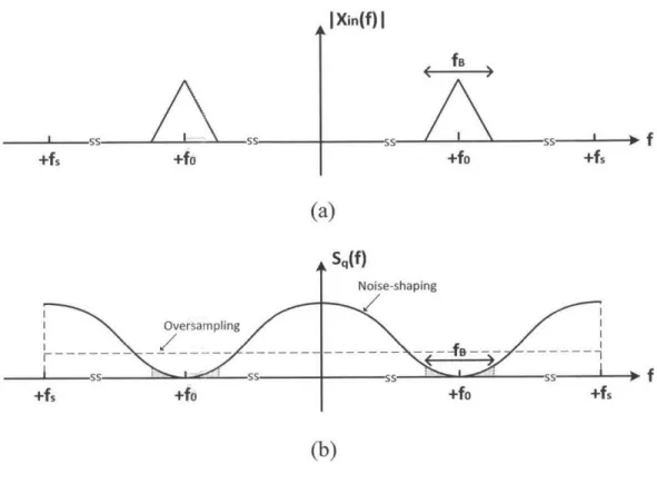
For bandpass modulators, however, narrow-band signals are centered at a carrier frequency fo. fB now represents the double-sided bandwidth of the signal.Figure 2-10(a) shows the spectrum of a bandpass input signal. In this section, we look at how this bandpass signal is oversampled and noise-shaped.
In order to oversample the bandpass signal,
f,
needs to be much higher than fB.The definition of OSR = f still holds. However, it is not, necessary that 2fB
f,
is much greater than fo. Thus, it is possible that the signal is comparable in frequency tof,
even though it is highly oversampled.In order to shape the quantization noise, we need to make the NTF a band-stop filter so that the quantization noise around fo is suppressed. This necessitates a bandpass loop filter L1(z). In fact, the only difference between a lowpass and
bandpass AE modulator is the type of loop filter that is employed.
Figure 2-10(b) illustrates the combined effect of oversampling and noise-shaping in the bandpass case. Most of the conclusions that we have drawn from the lowpass
+6 IXin(f)I fB +fo
(a)
Oversampling +s +fss +f F. + Sq(f) Noise-shaping /O +fo+s (b)Figure 2-10: (a) Spectrum of a bandpass input signal. (b) PSD of shaped quantization noise for a bandpass AE modulator.
2.3
Modulator Implementation
Now that we understand the principles of AE modulation, we examine in this section two types of AE modulators, namely DT and CT modulators. The major difference between the two types of modulators lies in the nature of the loop filter.
2.3.1
Discrete-time Delta-Sigma Modulator
A DT AE modulator processes the signal entirely in the discrete-time domain. This
necessitates an AAF and an S/H circuit that precede the modulator. Figure 2-11 shows the block diagram of the entire DT AE ADC [2]. The analog input signal, xmn(t), is filtered and sampled first before entering the DT AE modulator. The output signal from the modulator, v[n], contains both the input signal and the shaped
DTAZ Modulator Decimator
AAF
Loop Filter i Digital Filter
->t S/ H n]z Q uantizer v n
& s/ +jo L1(z)
R
Figure 2-11: Block diagram of a DT AE ADC [2].
zation noise at the rate of
f,.
A decimator that succeeds the modulator down-samplesv[n] to Nyquist rate, making the output signal from the ADC, y[n], compatible with
the digital blocks that follow.
The transfer function of the DT loop filter can be easily derived from the desired
NTF:
1
L1(z) = 1 - (2.20)
NT F(z)
In actual implementation, L1(z) and Lo(z) share the same hardware. Once we fix
Li(z), Lo(z) is determined. The STF of the modulator is thus:
STF(z) = 1 z) = Lo(z) - NTF(z) (2.21) 1 - Li(z)
The DT loop filter is usually implemented with switched-capacitor (SC) circuits that are accurate and robust under process variations. However, SC circuits require op amps to settle within half the sampling period. The gain-bandwidth requirements of the op amps are usually several times higher than
f,.
This makes DT implementation unsuitable for high sampling rate (~ GHz) and wide-band (-10 MHz) applications.2.3.2
Continuous-time Delta-Sigma Modulator
The loop filter of a CT AE modulator operates in a continuous-time fashion. Figure 2-12 shows the block diagram of an overall CT AE ADC [2]. Apart from the nature of the loop filter, a significant difference between CT and DT AE ADCs lies in the point
CTIX Modulator Decimator
Loop Filter Quantizer Digital Filter Xin()
Loc~) -+S/H+ --
R fS
DAC
-Figure 2-12: Block diagram of a CT AE ADC [2].
where sampling takes place. The signal in the CT AE ADC remains continuous until it reaches the quantizer, where both sampling and quantization happen at the same time. The simultaneous sampling and quantization provide a CT AE modulator with an inherent anti-aliasing filtering characteristic. The frequency components that are to be aliased in-band, as well as the quantization noise, are filtered by the NTF and are thus suppressed. The AAF can thus be removed from the ADC, which saves both power and system hardware.
The CT loop filter can be realized with gm-C or active-RC filters. These filters do not require op amps to settle. This greatly relaxes the gain-bandwidth requirements of the op amps and thus reduces the power consumption of the modulator. The speed of a CT AE modulator is limited by the excess delay through the op amps, the regeneration time of the quantizer, and the update rate of its DACs [1]. This enables the CT AE modulator to function at a much higher sampling rate with a much wider signal bandwidth compared with its DT counterpart. Because of its potential of fast operations and power efficiency, CT AE modulators provide a good solution for high speed and wide-band analog-to-digital conversion.
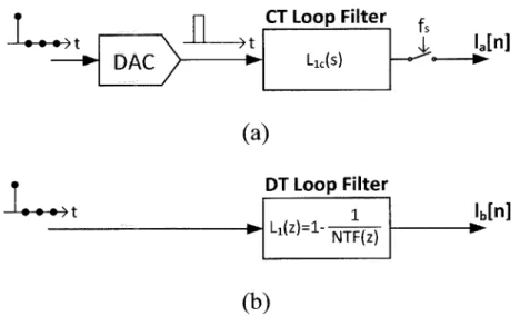
The transfer function of the CT loop filter, Loc(s), is difficult to determine now that the modulator travels between discrete- and continuous-time domains. Besides, the behavior of the DAC affects the loop as well. To solve this problem, we introduce the impulse response matching method [1].
Loop Filter Quantizer
u(t) -- o LOc(s)
- --q(Z _ -_ v[n]
Figure 2-13: Block diagram of a CT AE modulator incorporating the equivalent DT
loop transfer function Lieq (z)
2.3.3 Impulse Response Matching
The output of the CT AE modulator is a DT signal. We can thus derive a equivalent DT loop transfer function of the CT modulator:
Leq(z) =Z L-1[DAC(s)Lc(s)] [Z6(t - nT) (2.22)
n=O.
where T = is the sampling period, and the periodic impulse train models the
T,
sampling procedure.
Figure 2-13 shows the block diagram of a CT AE modulator incorporating Lieq(z).
The NTF and STF of the CT AE modulator are expressed in Equations 2.23 and 2.24
respectively: 1 NTF(z) 1 (2.23) 1 - Lieq(Z) ST F(s) = O(s = Loc(s) - NT F(z) (2.24) 1 - Lieq(z)
By looking at Equation 2.24, we can observe the anti-aliasing filtering characteristic
of the STF from the NTF(z) term it contains.
Equation 2.22 is very complicated and difficult to solve. A practical way to de-termine Lieq(z) is to find its impulse response. We do tiis by breaking the feedback loop at the quantizer, inserting an impulse at the output, and sampling the signal
CT Loop Filter li DAC Llc(s)
0-(a)
DT Loop Filter L1(z=1-NTF(z)(b)
Figure 2-14: Impulse response matching method. (a) Impulse response of of the CT feedback path. (b) Impulse response of the equivalent DT loop filter.
that is coming back to the quantizer, as shown in Figure 2-14(a). The resulting 1a[n]
is exactly the impulse response of Lieq(z). In order to obtained Lic(s), the transfer function of the CT loop filter, we need a DT loop filter that gives the same NTF as that of the CT AE modulator. The transfer function of this DT loop filter, L1(z),
is expressed in Equation 2.20. We then adjust the coefficients of Lic(s) so that la[n] matches lb[n], the impulse response of L1(z). The resulting Lic(s) is the CT loop filter transfer function that gives the desired NTF.
2.4
Summary
This chapter mainly covers two topics: (a) the principles of AE modulation, and (b) the comparison between D' and CT AE modulators.
Compared with its DT counterpart, a CT AE modulator is capable of a higher sampling rate, a wider signal bandwidth, and better power efficiency. It also has an inherent anti-aliasing filtering characteristic that removes the AAF from the system. Thus, a CT bandpass AE modulator provides a promising solution for modern
soft-CT Loop Filter
u(t) Quantizer
A v[n]
Resonator
UeS) fs
Figure 2-15: General block diagram of a CT bandpass AE modulator
ware receivers. A general block diagram of a CT bandpass AE modulator is shown in Figure 2-15.
Now that we have described the basic operations, the following chapters will dis-cuss the implementation of a CT bandpass AE modulator from both system-level (Chapter 3) and transistor-level (Chapter 4 and 5) points of view.
Chapter 3
Modulator Architecture
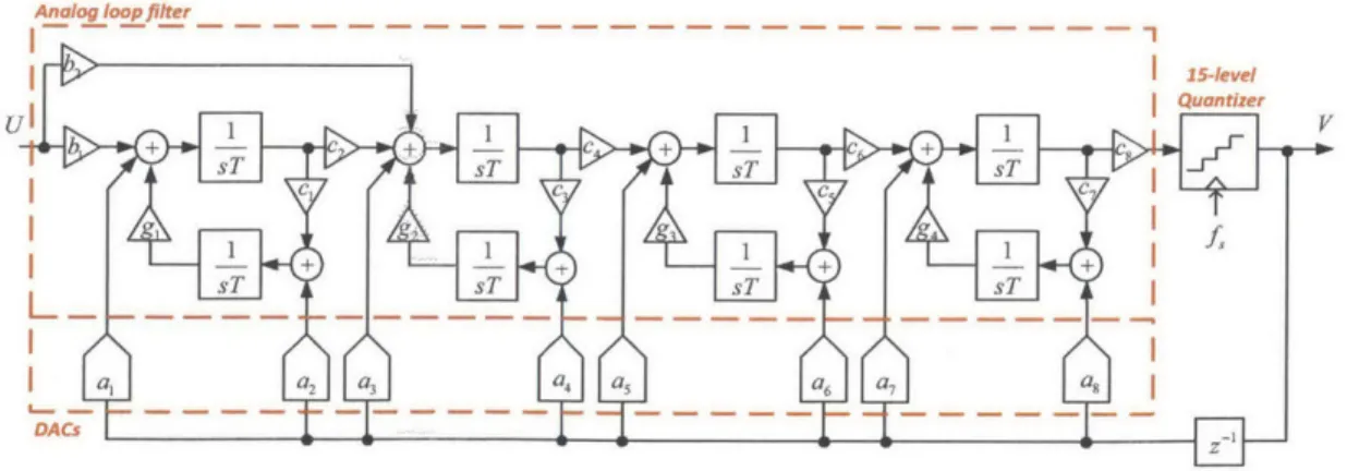
This chapter describes the system-level design methodology of the CT bandpass AE modulator. We first introduce the procedure of determining the modulator specifica-tions. Based on these targets, a proper NTF is selected and its realization examined. Two different modulator architectures, the feedback and the feed-forward, are dis-cussed and compared. The feedback topology is chosen due to its greater stability, better STF, and superior anti-aliasing filtering property. We modify the modulator topology by adding a feed-forward coupling path so that the distortion is reduced and the modulator linearity is improved. We then introduce the method of determining the various coefficients of the modulator that implement the desired NTF.
Analog loop filter
Quantizer
U1 1
L--- --- ---
---I g 32 b aa ose
A complete block diagram of the proposed CT bandpass AE modulator arrives
at the end of the chapter and is displayed here first in Figure 3-1
3.1
Desired Modulator Specifications
The goal of this thesis is to demonstrate a wide-band, high-resolution, and power efficient CT bandpass AE modulator that is suitable for software-defined receiver systems. Table 3.1 lists the desired specifications of the modulator. The procedures of determining these specifications are stated as follows.
Table 3.1: Desired modulator specifications.
Parameter Desired Specification Modulator Architecture Continuous-Time
Feedback Topology Sampling Frequency
(fU)
1 GHzSignal Bandwidth (fB) 25 MHz
Center Frequency (fo) 250 MHz (
)
Oversampling Ratio (OSR) 20 Signal-to-Noise Ratio (SNR) 75 dBNumber of Quantization Levels (M) 15
Quantization Step (A) 120 mV Power Consumption 300 mW
For the modulator architecture, as explained in tie previous chapter, the CT type of AE modulator is more suitable for our application due to its high speed, wide bandwidth, and low power consumption capability. In Section 3.4, we will learn that the feedback topology has the benefits of greater stability and better anti-aliasing filtering in the presence of large out-of-band interferers. Both advantages render the feedback topology a better fit for receiver applications than its feed-forward counterpart.
In terms of modulator performance, the sampling rate should be on the order of GHz to achieve both a wide signal bandwidth of about 25 MHz, and a fair OSR,
which is necessary to achieve high resolution. An OSR of 20 is chosen arbitrarily in this design, mandating the sampling frequency to be 1 GHz. For the center frequency
fo,
we place it at f for the following considerations:* The image signals affect the in-band signal to a minimal degree when fo = f.
" Digital down-conversion becomes much easier to implement when fo = f.4.
" The coefficient of the direct feedback path around the quantizer becomes zero
when fo - L, eliminating the DAC with the most stringent speed requirement.4
In order to achieve high resolution, a SNR around 75 dB is targeted.
For the quantizer, we need finer quantization to achieve greater SNR. Meanwhile, the quantizer needs to operate fast enough so that the digital output signals can settle within half a sampling period. A 15-level quantizer is thus chosen as a fair trade-off between speed and resolution. The input range of the quantizer is dictated by be the maximum output signal swing that the loop filter is capable of. For a 1.2 V power supply and a push-pull output stage, the single-ended signal swing of the loop filter can reach as high as 900 mY, hence the differential input range [-900 mV, +900 Iv]. The LSB (or A) is thus calculated from Equation 2.1 to be 120 mV.
The target power consumnption of the modulator is found by scaling the power consumptions of recently pu lblished state-of-the-art CT bandpass AE modulators ([9]
[13] [14] [3]) in such a way that a similar FoM is achieved. The definitions of FoM
and ENOB are expressed earlier in Equation 1.1.
3.2
NTF Selection
For a well-designed AE moldulator, the SNR should be limited by thermal noise, and the quantization noise should be negligible. A SQNR of 90 dB is thus targeted in this design.
The SQNR of a AE modulator is determined by three factors: the OSR, the NTF, and the number of quantization levels. The OSR determines the signal bandwidth with respect to the sampling frequency. The NTF decides the extent to which the in-band quantization noise is suppressed. The number of quantization levels gives the
Pole-zero Plot Frequency Response 1 20 0 0.5 M -20-0 --- 40 E \ -60- -0.5-x x -80 --1 -100--1 -0.5 0 0.5 1 -0.5 0 0.5
Real(z) Normalized Frequency
Figure 3-2: Pole-zero plot and frequency response of the desired NTF.
amount of the quantization noise that is to be shaped by the NTF. Both the OSR and the number of quantization levels are pre-determined in the specifications. We need to select a proper NTF that achieves the target SQNR.
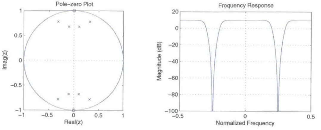
By using the delta sigma toolbox [16], an 8th-order NTF is chosen. Its expression
is displayed below:
NTF(z)=
(z2 + )4 (3.1)
(z2 + 0.20z + 0.47) (z2 - 0.20z + 0.47) (z2 + 0.64z + 0.71)(z 2 - 0.64z + 0.71)
The pole-zero plot and the frequency response are displayed in Figure 3-2.
The 8th-order NTF places four of its zeros inside the signal band and the other four in the image band, making possible a 4th-order noise-shaping. All the zeros are located at band center. Although, by optimally spreading the zeros across the signal band, a theoretical SQNR improvement of 10 dB can be achieved, the final SNR of the implemented modulator, which is thermal noise and distortion limited, can hardly be affected by this improvement. Therefore, to simplify the design, we position all the NTF zeros at band center. The maximum out-of-band gain (Hagf) of this NTF is 3, which achieves a fair trade-off between stability and the achievable SQNR.
Figure 3-3: Block diagram of a CT resonator.
3.3
Realizing Complex NTF Zeros
Equation 3.1 shows that the desired NTF contains eight zeros at ty. These ze-ros translate into poles of the loop filter L,(s). We employ resonators as shown in Figure 3-3 to implement these poles. The transfer function of the resonator is:
sT
Tres(S) = (3.2)
(sT)2 + g
where T = - represents the sampling period.
The value of g affects the pole locations directly. Since the center frequency is at
f, the poles of Tres (s) need to be placed at t2'If3. We can thus calculate the value
of g to be (i)2 or 2.467.
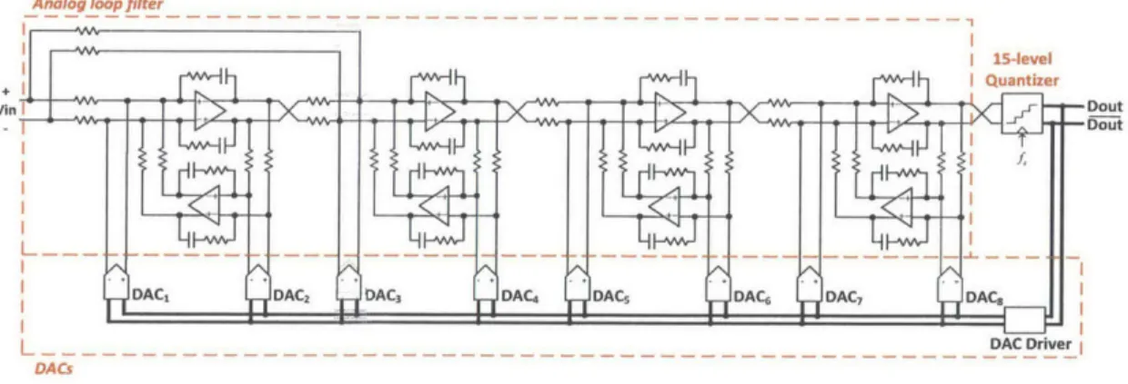
The type of resonator shown in Figure 3-3 forms the building block of the modula-tor loop filter. In our design, four of them are cascaded to realize the 8th-order NTF. Since two integrators are required to realize one resonator, the whole modulator in turn necessitates eight integrators or eight op amps.
3.4
Modulator Topology
Now that the NTF is chosen, we need to consider the implementation of the modu-lator. Two commonly used modulator topologies are the feed-forward and feedback topologies, whose block diagrams are illustrated in Figure 3-4 and Figure 3-5
respec-Figure 3-4: Block diagram of an 8th-order feed-forward CT bandpass AE modulator.
15-level Quantizer
U b + c, + c c + c . + -T c J
DA -1
Figure 3-5: Block diagram of an 8th-order feedback CT bandpass AE modulator.
tively. Each topology has its own advantages and disadvantages, which are discussed
and compared in this section.
3.4.1
Feed-forward Versus Feedback Topology
For the feed-forward topology, the major advantage is its low power consumption. The modulator has only one feedback path. At the input summing point, the signal components get cancelled almost entirely, and the loop filter receives only the shaped quantization noise. This largely reduces the dynamic range requirement of the loop
filter, hence lowering power consumption.
The feedback topology, on the other hand, contains multiple feedback paths. Therefore, each resonator possesses the signal componets that are yet to be
can-STF for Feedback and Feedforward Topology 20 20 --40 - - -60-' -80 --100 - - --120 --140 Feedback Topology Feedforward Topology 0 0.5 1 1.5 Normalized Frequency
Figure 3-6: STF of both feedback and feed-forward topology.
celled by the succeeding feedback path. The dynamic range requirement of the loop filter thus becomes more strict, with that of the 1st resonator being the most stringent.
Therefore, the loop filter of the feedback topology is very power hungry. Besides, the feedback topology requires a couple of DACs in its feedback path whereas its feedfor-ward counterpart needs only one. This again accounts for more power.
Nevertheless, the STF of the feed-forward topology is problematic. Figure
3-6 compares the STF of a feed-forward CT AE modulator with that of a feedback
modulator which realizes the same NTF. Inside the signal band, both STFs are flat at OdB, which is desirable. Outside the signal band, however, the STF of the feed-forward topology suffers from. two serious problems:
Large out-of-band peaking The STF of the feed-forward topology has an
out-of-band peaking of 10 dB. This makes the feed-forward modulator much more likely to go unstable, especially in the presence of large out-of-band interferers. Even without out-of-band interferers, behavioral-level simulations show that the maximum stable input amplitude of the feed-forward topology is 4 dB lower than that of its feedback counterpart. This essentially means a 4 dB degradation in SNR.
Poor anti-aliasing filtering characteristic The anti-aliasing filtering
charac-teristic of the feed-forward topology is much worse than that of its feedback counter-part. At the band edge, especially, the alias attenuation of the feed-forward topology
is only 60 dB. This is 50 dB lower that the attenuation from the feedback topology, and is highly insufficient.
The reason for the poor STF of the feed-forward topology is explained as follows. From Equation 2.24, we learn that the STF is the product of the CT loop filter transfer function Loc(s) and the NTF. Inside the signal band, the zeros from the
NTF are cancelled by the poles from Loc(s), which gives a flat and unity in-band
gain. In the image bands (i.e. in the vicinity of 3f and f), the STF is dominated by the NTF. The image signals inside these bands are thus suppressed, hence the
inherent anti-aliasing filtering property. Outside the signal and image bands, the
STF is dominated by Loc(s). For the feedback topology, the Loc(s) gives four zeros
at DC. Therefore, from DC to the signal band, the STF ramps up at 80 dB/dec; from the signal band to higher frequencies, it rolls off at -80 dB/dec. For the feed-forward topology, on the other hand, the multiple feed-feed-forward paths in the loop filter create zeros in the vicinity of the signal band. This reduces the effective order of the
STE. Therefore, the STF ramps up and down much more slowly than its feedback
counterpart, resulting in insufficient alias attenuation. These zeros around the signal band are also the cause of the large out-of-band peaking.
Apart from STF problems, an additional summing op amp is needed in the feed-forward topology between the loop filter and the quantizer. This is undesirable be-cause the summing block introduces additional excessive loop delay (ELD) and may adversely affect the stability of the modulator.
Considering the factors above, we choose the feedback topology for our design. Despite greater power consumption, the feedback topology provides greater stability and a much better STF that is free from out-of-band peaks and allows decent alias at-tenuation, both of which are advantageous in the context of wireless communications where large blocker signals are present [3].
One thing to note here is that there is always a delay block associated with the quantizer on the modulator block diagrams. This is because the outputs of the quantizer are latched and become only available after one clock cycle delay. The
15-level Quantizer
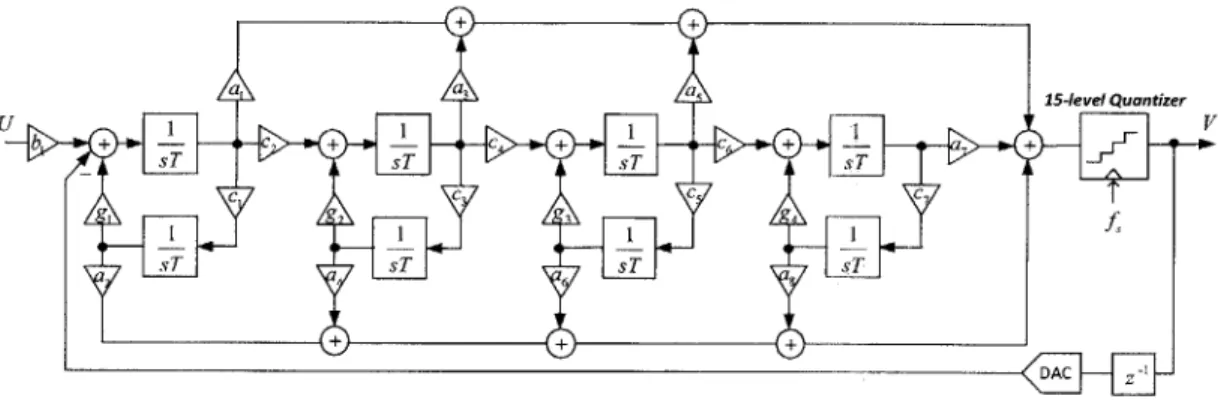
b + + + A
Figure 3-7: Block diagram of the modified modulator topology.
latch is necessary since it helps avoid the metastability issues of the quantizer [17] and synchronizes the quantizer output with the clock. By adding this latch, the delay of the quantizer is fixed and well-modeled.
3.4.2
Modified Feedback Topology
As discussed later in Section 4.1.2, the thermal noise from the Pt resonator is a limiting factor for the achievable SNR of the modulator. Our solution to this problem is to boost the signal swing of the 1st resonator by employing a dual 2.5-V/1.2-V power
supply. The signal swing at the output of this resonator thus gets doubled, offering a SNR improvement of 6 dB. However, the distortion from this resonator becomes the new limiting factor.
In an effort to alleviate the distortion, a feed-forward coupling path with the coef-ficient b2 is added, as shown in Figure 3-7. Since this path provides another channel
for the input signal to travel, the signal components carried by the 1st resonator is
re-duced, thereby relaxing the swing requirement and easing the distortion. Besides, the coefficient b1 can be made larger now that the signal components in the 1St resonator
become less. As introduced later in Section 4.1.2, increasing b1 further improves SNR.
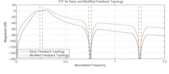
This additional feed-forward coupling path does not affect the NTF of the modu-lator. However, the STF is altered depending on the value of b2. Figure 3-8 compares