A Continuous Time Sigma-Delta Modulator for
Digitizing Carrier Band Measurements
by
Philip Weimin Juang
Submitted to the Department of Electrical Engineering and Computer
Science
in partial fulfillment of the requirements for the degree of
Master of Engineering in Electrical Engineering and Computer Science
at the
MASSACHUSETTS INSTITUTE OF TECHNOLOGY
June 2001
©
Philip Weimin Juang, MMI. All rights reserved.
The author hereby grants to MIT permission to reproduce and
BARKER
distribute publicly paper and electronic copies of this thesis d
S NSTITUTEin whole or in part.
OF TECHNOLOGYJUL 1 1 2001
LiBRARIES
Author ... ....
Department of Electrical Engineering and G iiiuter Science
May 11, 2001
Certified
by...
James K. Roberge
Professor of Electrical Engineering
\ Thesis Supervisor
Certified by...
...
R\bert'Bousquet
C.S. Draper Laboratoryenior Engineer
Thi's SujpAgDVisor Accepted by . ..
Arthur C. Smith
Chairman, Department Committee on Graduate Theses
MITLibraries
Document Services Room 14-0551 77 Massachusetts Avenue Cambridge, MA 02139 Ph: 617.253.2800 Email: [email protected] http://libraries.mit.edu/docsDISCLAIMER OF QUALITY
Due to the condition of the original material, there are unavoidable flaws in this reproduction. We have made every effort possible to provide you with the best copy available. If you are dissatisfied with this product and find it unusable, please contact Document Services as soon as possible.
Thank you.
Some pages in the original document contain text that runs off the edge of the page.
A Continuous Time Sigma-Delta Modulator for Digitizing
Carrier Band Measurements
by
Philip Weimin Juang
Submitted to the Department of Electrical Engineering and Computer Science on May 11, 2001, in partial fulfillment of the
requirements for the degree of
Master of Engineering in Electrical Engineering and Computer Science
Abstract
This document discusses the design of a low power, low area, sigma-delta modulator to be built on a .5pm CMOS process. First, the use of a continuous-time topology is investigated and compared with an existing discrete-time design. Next, the de-sign methodology of a 3rd-order continuous-time modulator is explored; the same methodology is then applied to a 4th-order modulator design. Both designs were fabricated and tested in the lab. The final section discusses the test results from the completed IC's and comments on the viability of continuous-time modulators for this application.
Thesis Supervisor: James K. Roberge Title: Professor of Electrical Engineering Thesis Supervisor: Robert Bousquet
Acknowledgments
First and foremost, I'd like to thank my thesis supervisors, Professor James K. Roberge and Rob Bousquet, as well as all of my friends and colleagues at Draper Laboratory: Paul Ward, Eric Hildebrant, Bill Kelley, Tom King, Shida Martinez, Chris O'Brien, and Rob Bousquet. They have all made my career at MIT and Draper fun and worthwhile. My understanding of electrical engineering in general and solid-state circuits in particular has benefited from their endless patience and invaluable counsel. I am tremendously grateful for their contributions to my professional growth. Second, I'd like to acknowledge my friends, who have stood by me throughout my years at MIT and have provided welcome relief after the long days of thesis writing. Thanks go out to Stimpe, Steve, Keith, Jon, Frank, Morris, Spencer, Lahaie, Ryan, Amar, and of course, Christine.
Lastly, I'd like to extend thanks to my parents for their love and support. I am in their debt, as without their patience and wisdom, I might have become a chemical engineer. I hope they enjoy reading the next 100 pages.
This thesis was prepared at The Charles Stark Draper Laboratory, Inc., under Internal Company Sponsored Research No. C312.
Publication of this thesis does not constitute approval by Draper or the sponsoring agency of the findings or conclusions contained herein. It is published for the exchange and stimulation of ideas.
Permission is hereby granted to the Massachusetts Institute of Technology to reproduce any or all of this thesis.
Contents
1 Introduction
1.1 Background .... ...
1.2 O utline. . . . . 2 Fundamental Operation of E-A Modulators for
Conversion
2.1 Characteristics of E-A Converters . . . .
2.1.1 Oversampling Converters . . . .
2.1.2 Noise Shaping . . . .
2.2 A Discrete-Time Third Order E-A Modulator . .
2.2.1 Basic Modulator Operation . . . .
2.2.2 Circuit Realization . . . .
3 Advantages and Disadvantages of Continuous-Time E-A
3.1 B enefits . . . .
3.1.1 Reducing power consumption . . . .
3.1.2 Decreasing chip area . . . .
3.1.3 Lowering thermal noise . . . .
3.2 Drawbacks . . . .
3.2.1 Absolute component tolerances . . . .
3.2.2 Sample-and-hold circuit . . . . 3.2.3 Return-to-zero DAC . . . . 3.2.4 Clock Jitter . . . . 17 17 18 Analog to Digital Modulators 21 21 22 26 31 32 33 39 39 40 41 43 46 46 47 47 48
4 Design of a third-order continuous-time E-A modulator
4.1 Design possibilities . . . .
4.1.1 Direct impulse-invariance transformation . . . .
4.1.2 Tunable on-chip components . . . .
4.1.3 Continuous-time front end . . . ..
4.1.4 Lowpass modulator topology . . . .
4.2 Design Methodology . . . .
4.2.1 Initial hand design . . . .
4.2.2 Software simulation design . . . .
4.2.3 1-bit Return-to-zero Digital-to-Analog Converter
4.3 Design Review . . . .
4.3.1 Simulated Performance . . . .
4.3.2 Weaknesses . . . .
5 Design of a fourth-order continuous-time E-A modulator
5.1 Techniques to decrease quantization noi
5.1.1 Increasing sampling frequency .
5.1.2 Fourth-order topology . . . . .
5.2 Design methodology . . . .
5.2.1 Initial hand design . . . .
5.2.2 Minimizing power consumption
5.2.3 RTZ DAC redesign . .. . . . 5.3 Design Review . . . . 5.3.1 Simulated Performance . . . . . 5.3.2 Analysis . . . . 3e . . . . 7 7 . . . . 7 7 . . . . 7 8 . . . . 7 9 . . . . 7 9 . . . . 8 1 . . . . 8 2 . . . . 8 3 . . . . 8 3 . . . . 8 7
6 Measurement Results of On-chip Continuous Time
6.1 Measured performance . . . .
6.1.1 SD3CT measurements . . . .
6.1.2 SD4CT measurements . . . .
6.2 Effects of Clock Jitter . . . .
E-zA Modulators 89 89 89 91 94 53 . . . . 53 . . . . 53 . . . . 55 . . . . 55 . . . . 57 . . . . 58 . . . . 58 . . . . 64 . . . . 69 . . . . 70 . . . . 70 . . . . 75 77
6.2.1 Phase noise modulation . . . .
6.2.2 Clock jitter tolerances for SD3CT and SD4CT . . . .
6.3 Future W ork . . . .
7 Conclusion
A Circuit Schematics of SD3CT and SD4CT B SD3CT Simulation and Lab Test Data C SD4CT Simulation and Lab Test Data D Clock Jitter Test Results
95 96 98 101 103 109 119 129
List of Figures
1-1 Power spectrum of analog input signal . . . .18
2-1 A 1-bit oversampling converter . . . . 22
2-2 Spectrum of x[n], sampled from continuous-time signal x(t) . . . . 23
2-3 White noise model of quantizer . . . . 23
2-4 Spectral Density of e[n] . . . . 24
2-5 Spectral Density of r[n] . . . . 25
2-6 Brick wall filter used to attenuate the out-of-band noise . ... . . . . . 25
2-7 Spectral Density of y[n]. All the out-of-band noise has been filtered out. 26 2-8 A 1-bit oversampling converter with noise shaping . . . . 27
2-9 Noise shaping loop with the white noise model of the quantizer . . . . 27
2-10 Frequency Response of H(ejw) (single integrator) represented in log scale. 28 2-11 Signal Transfer Function: X(ejh')P(ejw) represented in log scale. . . . . 29
2-12 Noise Transfer Function: P(ew) E(ejw) 1represented in log scale. . . . . 29
2-13 Noise Spectrum: Spectrum of P(ei") due to E(ew). The dotted line represents the spectral height ke of the error signal. The solid line depicts the error signal after noise shaping. . . . . 30
2-14 Noise Spectrum: Spectrum of P(ejw) due to E(ew) after filtering. The two components are the same as in Figure 2-13. Note that the spectral density of the shaped noise is significantly reduced. . . . . 31
2-15 Block diagram of third order EA circuit. . . . . 32
2-16 Frequency Response of the Noise Transfer Function with f, = 5.12MHz. 33 2-17 A fully differential switched-capacitor integrator . . . . 34
2-18 1-bit feedback DAC as it is implemented in the existing third order m odulator design . . . .
3-1 A simple continuous-time integrator (fully-differential) . . . .
3-2 Block diagram of third order EA circuit. . . . .. . . . . 3-3 Two waveforms with 7 "ones." Due to rise and fall times, the energy
(area under the curve) in the first waveform is slightly different than the energy in the second. . . . . 3-4 Waveform of a Return-to-Zero DAC. . . . . 3-5 Feedback current waveforms for a single sampling period . . . .
3-6 Clock jitter effects on the current waveforms of two different DAC
im plem entations. . . . . 4-1 4-2 4-3 4-4 4-5 4-6 4-7 4-8 4-9 4-10
Change in notch frequency with a 25% variance in c4 . . . . Block diagram of third order EA circuit. . . . .
Block diagram of a third order lowpass EA modulator. .
Frequency Response of the NTF with all poles located at u frequency 1.28M Hz . . . . Bode plot of hand designed loop gain . . . . Magnitude response of the NTF corresponding to Figure 4-5 Root locus plot of the loop transmission . . . .
Circuit simulation of lowpass third order modulator . . . . . Output of integrator 2 using initial hand design . . . .
Output of integrator 2 with decreased feedback coefficient b2
. . . . 55
. . . . 56
. . . . 59
nity-gain
4-11 Block diagram of third order lowpass EA modulator with feedforward paths. . . . .
4-12 Output of integrator 2 with decreased feedback coefficient b2 and
feed-forward path from x[n] . . . . 4-13 Circuit diagram of a monostable multivibrator (one-shot) . . . . 4-14 Transmission gates that switch the feedback node from NREF, MID,
and PREF... ... 37 40 43 48 49 49 51 60 62 63 63 64 65 66 67 68 69 70 .
Positive and negative return-to-zero pulses generated by the DAC Plot of SD3CT Noise Transfer Function . . . .
Power spectrum of SD3CT output, normalized to P,=1V2
71 73 74
Bode plot of the hand designed fourth-order loop gain . ... . . . . 80
Frequency Response of the NTF corresponding to Figure 5-1 . . . . . 80
Root locus plot of the fourth order loop transmission . . . . 81
Circuit implementation of the redesigned DAC . . . . 83
Return-to-zero waveforms for the redesigned DAC . . . . 84
Magnitude response of the SD4CT noise transfer function . . . . 85
Power spectrum of the SD4CT output, normalized to P'=1V2 . . . . 86
5-1 5-2 5-3 5-4 5-5 5-6 5-7 6-1 6-2 6-3 92 93 95 4-15 4-16 4-17
Nominal output spectrum of SD4CT . . . .
Nominal output spectrum of SD4CT (zoomed out) . . . .
Output spectrum of SD4CT using a clock with white jitter
List of Tables
1.1 Specifications for A/D conversion of input signal . . . . 19
6.1 Measured performance for A/D conversion using SD3CT . . . . 90
6.2 Measured performance for A/D conversion using SD4CT . . . . 91
6.3 Relationship between clock jitter and output noise floor for SD3CT 97
Chapter 1
Introduction
1.1
Background
The Microelectronics Group at Charles Stark Draper Laboratories has a need to digitize an analog waveform for digital processing. The signal of interest is bandlim-ited to 100Hz and modulated on a sinusoid whose frequency is 2f, (nominally 20kHz). Figure 1.1 approximates the power spectrum of the analog input; the signal of in-terest is located about the second harmonic. While this signal can be extracted and processed using analog circuitry, significant error can be introduced by DC bias drift. It has been shown that digital processing of the signal results in the elimination of this problem.
A sigma-delta (E-A ) A/D converter is suited to the task of digitizing the signal, due to its ability to achieve high-accuracy data conversions in a relatively short pe-riod of time. Furthermore, since the linearity of the conversion is important to this application, E-A converters are well suited to this job A 3rd-order discrete-time (DT) E-A modulator has been designed and fabricated on a CMOS process to perform this task. The device is powered by a single 5V supply-all other voltages needed are gen-erated on chip. The input signal is centered about a virtual ground of 2.5V (which we designate MID). Table 1.1 displays the major specifications of a E-A modulator, as well as the measured results obtained from a discrete-time design [10].
f,
nominally 10kHzfo 2fo 3fo 4fo
Figure 1-1: Power spectrum of analog input signal
this is somewhat problematic, it has been found that this E-A modulator functions adequately; the specification is somewhat conservative. Since all other specifications appear to have been met, it will be used as intended. However, we foresee a need for a smaller, lower power A/D converter that can achieve the specified noise level in future applications. For this reason, we are interested in investigating new E-A designs; of particular interest to us is a continuous-time topology. It is believed that such a design will be useful for future ASICs.
1.2
Outline
Usually, E-A modulators are designed using a DT topology, employing the use of switched-capacitor filters when implemented. The goal of this thesis is to explore the use of a continuous-time (CT) implementation for our specific need. We begin by discussing the operation of E-A converters, the principle of oversampling, and the techniques involved in noise shaping. We will also highlight the major advantages and limitations of CT E-A modulators and explore its use for digitizing our carrier band measurement. As we shall see, using a CT E-A modulator is extremely beneficial in terms of reducing power consumption and minimizing circuit noise.
The next part of this document will focus on the design of a 3rd-order CT mod-ulator. We will see that the most difficult tasks are achieving sufficient quantization
Characteristic Specification Result
Clock Frequency 256*fo
Full Scale SNR within 20kHz+100Hz 117 dB 111 dB
Input Range > 1 V Full scale + 2.5V FS
Second Harmonic Distortion < -80dBcFS . -82dBcFS
(from 10kHz input)
AC Gain Stability at 20kHz 1% over 0.4% over
temperature temperature
Spurious Tones < -80dBcFS No tones in
at 20kHz+4kHz output spectrum
Power Consumption 40mW
Chip area - 9mm2
Table 1.1: Specifications for A/D conversion of input signal
noise shaping, eliminating the factors changing the scale factor of our modulator (i.e. maintaining AC gain stability), and minimizing the effects of clock jitter, which injects undesired noise into the system. A 3rd-order modulator is found to be insuffi-cient for our needs; hence, we then discuss a 4th-order design while addressing issues uncovered in the 3rd-order modulator.
Finally, we compare our expected results to those obtained from lab testing of the manufactured silicon test chips. The last section discusses the discrepancies discov-ered, studies and documents the effects of clock jitter on our modulator, and suggests future work to be done on this topic.
Chapter 2
Fundamental Operation of E-A
Modulators for Analog to Digital
Conversion
2.1
Characteristics
of
E-A
Converters
E-A converters are generally defined to be the class of converters which use shaped quantization noise with oversampling to achieve high resolution. E-A conversion has become popular for many reasons [2]:
* It yields high accuracy results fairly quickly; thus, it is useful for high-resolution, medium speed applications.
9
It is easily realized on a CMOS process. Often, E-A converters rely onwell-matched components, which are provided on an integrated circuit.
* A/D converters are usually preceded by an anti-aliasing filter. E-A converters reduce the required performance of these filters.
* The static power dissipation can be made very low without significantly degrad-ing the performance of the converter.
fS
x[n] -r[n]
x(t) (e) [n]
Quantizer
Figure 2-1: A 1-bit oversampling converter
E-A conversion is done in two stages. The first stage samples the analog signal and shapes the quantization noise. The second stage downsamples the bits obtained from the first stage and digitally filters the out-of-band noise. This decimator is realized using digital circuitry. This document is mainly concerned with the design of the first stage, often called the modulator. Design of the second stage, called the
decimator, is beyond the scope of this thesis.
To fully understand the issues involved in designing E-A modulators, one must be familiar with the concepts of oversampling and noise shaping. This section will discuss these two techniques and illustrate them in a simple 1st-order modulator design.
2.1.1
Oversampling Converters
Oversampling is the method of sampling a signal above the Nyquist rate. It is a useful technique in A/D conversion, because it reduces the power of the quantization noise in the band of interest. To illustrate this effect, consider a 1-bit oversampling converter, whose block diagram is shown in Figure 2-1.
Let us suppose that x(t) is bandlimited to some frequency
fo.
The input signal x(t)is sampled at a frequency
f,
to produce a digitized signal x[n], whose power spectrumis shown in Figure 2-2. It is then put through a 1-bit quantizer to obtain an output
of either - or -$ (where A is equal to the difference in quantization levels). The
filter H(ew) serves to bandlimit the resulting output signal r[n] to some frequency
bandwidth
f.
The behavior of the quantizer causes an error (a significantly largeX(eij2n)
4
-fo
Z f
fo
Figure 2-2: Spectrum of x[n], sampled from continuous-time signal x(t)
e[n]
fS x[n] r[n]
x(t) , (e3') y[n]
Figure 2-3: White noise model of quantizer
be modeled as an additive white noise source (e[n]), as shown in Figure 2-3. [7] Intuitively, one can think of the quantization error sequence e[n] as being an independent random variable uniformly distributed between +A-since it is uniformly distributed, the spectrum will be flat. However, this approximation assumes that the quantization noise e[n] is uncorrelated with the input signal x[n]. In reality, these two signals have a small correlation; however, for hand calculations we can ignore this correlation and assume white noise. Thus, this model provides a good basis for estimating the signal-to-quantization-noise ratio (SQNR) of the A/D converter. This ratio is defined as follows:
P
SQNR =
--Pe (2.1)
where P, is the signal power at the output and Pe is the quantization noise power at the output. We can easily hand calculate these power values. First, if the input is a
Se (ej21r)
Height ke
2 2
Figure 2-4: Spectral Density of e[n]
sinusoid, the signal power at the output of an N-bit quantizer is given by [2]: A222N
PS = 8 (2.2)
For our example of a one-bit quantizer, N=1:
A2
PS=2 (2.3)
Pe can be easily calculated as well. As previously mentioned, we can model the
spectral density of e[n] (which we designate Se(f) as white noise (Figure 2-4). The total quantization noise power is known to be 4 [2], so the spectral density height,
ke, of the error signal can be calculated to be:
/f3/2
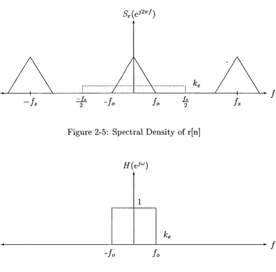
IS f, '2 Se( f) 2 df =ke2 -= (2.4) J-f8/2 12 A2 1 k 2 f (2.5) e12 fsWe have examined the spectrum of both x[n] and e[n], so we can determine what the spectral density of r[n] looks like; we denote this spectrum to be S,(f), which is shown in Figure 2-5. The triangle is the component due to the signal x[n] (which represents the signal power P,). The flat box is the component due to the quantization noise e[n] (which represents the signal power Pe and has spectral density height ke). The lowpass filter H(e'w) (shown in Figure 2-6) serves to attenuate the out-of-band
Sr (ej2 7rf)
4
2h -fo f I 2
f
Figure 2-5: Spectral Density of r[n]
H(ew)
-fo
1 kef
foFigure 2-6: Brick wall filter used to attenuate the out-of-band noise
noise. Since the x[n] is already bandlimited to
f
0, the signal power remains unchanged.However, the out-of-band quantization noise is filtered out, so the quantization noise power in y[n] is:
Pe = Se(f)2 IH(e ) 2f = f Se(f) 2df = k 2df 32
-1f12 -fo -f 12 f (2.6)
We define the term f,/2f0 as the oversampling ratio (OSR). Equation 2.6 shows
that the quantization noise power of y[n] is inversely proportional to the oversampling ratio. Hence, the OSR and the SQNR have the following relationship:
P _ A2 12 f SQNR= -- x =6 x OSR Pe 2 A2 2fo (2.7) b
Z:
-
fs
--- --- *---Sy (e)21rf
--- ... .* k e
f
-f0 fo
Figure 2-7: Spectral Density of y[n]. All the out-of-band noise has been filtered out.
SQNR(dB) = 10log(6) + 10log(OSR) (2.8)
So for every doubling of the oversampling ratio, the SQNR improves by approximately 3dB.
The spectral density of y[n] is depicted in Figure 2-7. It shows that through the use of oversampling, much of the noise power has been spread out across a wider band and then filtered out, thereby reducing the noise content in the output.
2.1.2
Noise Shaping
While oversampling is advantageous, it is usually not sufficient to obtain high-resolution A/D conversion. For example, in order for a 1-bit oversampling converter to achieve 70dB SQNR for a 20kHz bandlimited signal, a sampling frequency of 40GHz is required! One solution is to use multi-bit quantizers, which reduces the quantization error and thus the noise power. While achieving higher resolution with multi-bit quantizer architectures is possible, there are several drawbacks. First, the output of such an architecture would be a multi-bit word, instead of a single bit. This topology increases the complexity of the modulator; most notably, the D/A converter in the feedback path would require much more design work. Secondly, the FIR filter in the decimator would need to be able to handle multi-bit words, significantly adding to
x[n] , ~ s)-- r& Hen) y [n]
Quantizer
Figure 2-8: A 1-bit oversampling converter with noise shaping
e[n]
x~n ,. Les) rn] H (ejw) -y~n]
DAC
Figure 2-9: Noise shaping loop with the white noise model of the quantizer
of nonlinearity in the A/D conversion. The advantage of using a 1-bit converter is that it is inherently linear.
An alternative technique that is used to achieve a higher SQNR ratio is noise shaping. Noise shaping pushes the quantization noise out of band, so that it can be filtered out. The most common way of achieving this noise shaping is by feeding back the output of the quantizer to the sampled input, forming a feedback loop. The block diagram of this loop is shown in Figure 2-8. (Note: The D/A converter in the feedback path serves mainly to buffer the feedback signal and avoid loading the modulator output. In this case, it can be considered to be a unity gain block).
Using the white noise approximation for quantization noise (shown in Figure
2-9, it can be seen that the Signal Transfer Function (STF) and the Noise Transfer
50 40 - - - -10 - -.-2 0 -- --- -- - - . ...-- . --10 . . .. .. . . . . .. . . . . . . 5.. 1010,1 105
Figure 2-10: Frequency Response of H(ejw) (single integrator) represented in log scale.
TF-R(eiw) L(eiw)
STF = (ew) 1 L(eJw 1 f or L(eJw) > 1 (2.9)
X (ejw) 1 + L(ejw)
R(esw) _ 1
NT F - .ew) - 1(2.10)
E(ej) 1 + L(ew)
By choosing the magnitude of L(ew) to be significantly greater than 1 in the band of interest, the input signal x[n] will remain unaffected while the spectrum of the noise signal e[n] will be shaped so that the inband noise is attenuated. For example, choosing L(ejw) to be an integrator will have the desired effect-L(ew) has a large gain for low frequencies and small gain (less than unity) for high frequencies. This feedback structure, which provides the noise shaping, makes up a large part of E-A modulator design.
To illustrate this technique, let us assume that the input signal x[n] is bandlimited to 10kHz, and L(ew) is designed to be a single integrator with a unity-gain frequency of 20kHz. The STF is approximately unity at frequencies below 10kHz. The NTF attenuates the quantization noise error at low frequencies. Figures 2-10 through 2-12 show the magnitude responses in log-log scale.
-5
-10 - -.
-15
102 10 105
Frequency
Figure 2-11: Signal Transfer Function: X(ei-) represented in log scale.
0 -5 -10 -15 -20 -25 -30[ -40 -45 - -- - --- - - -a -- - 6 -m - - -... ---.... --..-..-..- . - -- - - --- --- -- - - -- a - - - -- - - --- - - -- -a - - -- -- - - - T - - - -m ---a--w -- --- - - - -- -- --- -w
Figure 2-12: Noise Transfer Function: represented in log scale.
103 Frequency 10 10 w w a m w ... m m w m m w w a m m m m w m a (D M CD 1 0 4 -35 [ 102
1 0.8 C 0.6 x1 0.4- 0.2--50 -40 -30 -20 -10 0 10 20 30 40 Frequency (kHz)
Figure 2-13: Noise Spectrum: Spectrum of P(eiw) due to E(ew). represents the spectral height ke of the error signal. The solid line signal after noise shaping.
50
The dotted line depicts the error
the input signal's spectrum by the square of the magnitude of the NTF Equation 2.6 can be rewritten to include the effects of the noise shaper:
Ifs/2
2 foPe = Se(f)2 NTF(f)H (ej27f) df = INTF(f)|2 k 2df
-fs / 2 J-f0
[7]. Hence,
(2.11)
Figures 2-13 and 2-14 show the two-sided spectrum of the modulator output P(e'w) due to the quantization noise error E(ejh) before and after filtering with a 10kHz brick wall filter. (For these figures, the spectral density height ke is arbitrarily chosen to be 1[V after oversampling.) It is easy to see that noise shaping has greatly reduced the noise power in the output; even for a first-order example, the noise power has been roughly reduced by a factor of 10 (20dB).
The characteristics of the noise shaper has a significant effect on the SQNR. While using a single integrator for L(eiw) provides a great deal of noise shaping, using two integrators can often provide more noise attenuation, especially at lower frequencies. Designing the filter L(ew) to be second order usually results in more noise shaping and better SQNR. However, second order feedback loops have the possibility of becoming unstable; hence, they must be designed to assure stability. Using three or more
0.8-0.6 ~-0.4-- 0.2-0 -50 -40 -30 -20 -10 0 10 20 30 40 50 Frequency (kHz)
Figure 2-14: Noise Spectrum: Spectrum of P(ew) due to E(ew) after filtering. The two components are the same as in Figure 2-13. Note that the spectral density of the shaped noise is significantly reduced.
integrators in the loop results in increasing improvements in SNR, but the tradeoff is that such high order modulators become increasingly difficult to stabilize.
This section has mainly discussed a 1-bit, single-stage architecture, as it is the focus of the E-A modulator designs to be presented in this paper. However, there are many other E-A modulator design topologies, including those which utilize multi-bit quantizers, multi-stage noise shaping (MASH), and interpolative structures to name a few. These designs are not discussed in this thesis.
2.2
A Discrete-Time Third Order
E-A
Modulator
The previous section discussed the techniques of oversampling and noise shaping as they apply to a baseband signal. Since we are designing a digitizer for carrier band measurements, our modulator should be designed for the passband. Recall that the
signal to be digitized lies in the spectrum of
f,
_100Hz (f, is nominally 20kHz). Thissection will discuss the topology of a previously designed third-order modulator for this application.
x[n] a1 a2 a3 ±Z + __-1 y[ni] 1-z Z + - 1 C3 b1b2 b3] DAC Figure 2-15: Block diagram of third order EA circuit.
2.2.1
Basic Modulator Operation
The block diagram for the modulator is shown in Figure 2-15. Note that it is
implemented in discrete time-the sampling frequency
f,
is set to be 256xfc (f, isnominally 5.12MHz). The STF and NTF are:
STF (a1 c1c2 - a2c2 + a3)z-3 + (a2c2 - 2a3)z-2 + a3z-1 (-1 - b3 + (b2 + c3)c2 - bicic2)z- 3 + (3 - c2(c3 + b2) + 2b3)z- 2 + (-3 - b3)z-1 + 1 (2.12) NTF = (1 - z- 1)(1 - 2z- 1 + (1 - c2c3)z- 2) (-1 - b3 + (b2 + c3)c2 - bicIc2)z- 3 + (3 - c2(c3 + b2) + 2b3)z- 2
+
(-3 - b3)z- 1 + 1 (2.13) The frequency response is shown in Figure 2-16 for the values of an, b", and c,, in this design. The poles and zeroes have been chosen so that the NTF contains a notch at f,/256, which is f. This notch serves to further attenuate the noise power at the frequency of interest, thereby increasing the SQNR.We can calculate the noise power at the output using Equation 2.11. Instead of
integrating over the interval -f0 to
f
0, we integrate over the passband intervalfc
-to
fc
+f
0.OSR= f = 25600 (2.14)
2 0- -20-S 4060 80 ---100 120 --140 110 10 10 Frequency (Hz)
Figure 2-16: Frequency Response of the Noise Transfer Function with
f,
= 5.12MHz.(- =5V)2 k2 -- f - 4.07 x 10⁻⁷ V2/Hz (2.15) e 12fs f+1OOHz k2
INTF(f)
2 df = 9.27 x 10- 20V2 (2.16) fc--100Hz P12.5 V 2 SQNR = 10log - = 10log = 201dB (2.17) Pe 6.03 x 10⁻¹³A SQNR of 201dB is extremely high. This resolution is much better than needed;
however, we will see in the following section that implementing the system introduces added noise sources which limit the performance of this modulator.
2.2.2
Circuit Realization
When we examine the distinctions between CT and DT topologies in the next chapter, we will find that most of the differences lie in the circuit realization of the
modulator. Therefore, it is important that we understand the implementation of
this particular modulator. Of particular interest is the switched-capacitor integrator circuit and the 1-bit DAC in the feedback path.
MID
I)
Cf 02 01 $N Ci 02 IN.- OUT IN, + OUT+ Ci 0 0JI
Cf MIDFigure 2-17: A fully differential switched-capacitor integrator
Switched-Capacitor Filters
The integrator blocks in the block diagram are realized using fully differential
switched-capacitor integrators, shown in Figure 2-17. There are several reasons for
using a fully differential structure. First, the input dynamic range is essentially doubled; since each input can span from OV to 5V, two inputs can span from OV to
10V when added together. Second, the differential output gain of the opamps can be
made to be stable over process and temperature variations; therefore, any common
mode DC offset in the input signal due to these changes will have little effect on the modulator performance, especially since the amplifiers and quantizer will effectively reject the common mode. The drawback of fully differential opamps is that they are usually larger in size and consume more power than single-ended designs (not to mention they are a little trickier to design).
The clock phases
#1
and 02 represent alternating control signals; when#
1 is ON,02 is OFF and vice versa. Assuming a 50% duty cycle, this circuit's input to output transfer function is that of a DT integrator (such as the ones used in Figure 2-15). Taking vn] to be the voltage across OUT+ and OUT-, vi[n] to be across IN+ and
VOW = _1 (Vi(z) - F(z)) (2.18)
C5 1 - Z-1
This circuit provides not only the integration, but also the summing node needed in the modulator. Since the feedback coefficients ai, bi, and ci are determined by the ratios of the input capacitors to the feedback capacitors of the integrators, the precise component matching of the CMOS process used in ASIC fabrication is a tremendous advantage when realizing these blocks. In fact, no part of this third order system is dependent on the absolute tolerances of any component; this characteristic is advantageous, because the on-chip capacitors in this fabrication process (.5pm CMOS) have an absolute tolerance of 8% in addition to a temperature coefficient of -25 ppm/C. The matching tolerance, however, is accurate to better than 1%. The bandwidth of the notch filter is wide enough to accomodate this matching error; hence, we are able to place the poles and zeroes of our system to reasonable degrees of accuracy.
This integrator circuit is also the key to understanding where thermal noise is generated. Examining the circuit, it can be determined that the sampling noise from the input capacitors (Ci) is the major source (the noise power density is given by
kT). Several capacitors on the input provide additive noise sources; hence, the
input-referred noise is high enough to be troublesome. Increasing the capacitor sizes will diminish the noise level-however, this translates into quite a bit more area needed on chip.
Experimentally, the thermal noise floor is measured to be approximately -I15dBc. The shaped quantization noise at 20kHz has been calculated to be much less than this value, so we can conclude that the limiting factor in the signal-to-noise ratio of this DT third-order modulator is thermal noise.
1-bit Digital to Analog Converter
At first glance, a 1-bit DAC does not appear to be useful at all. After all, a digital bit is represented by an analog voltage, so what is there to convert? Quite the
contrary, this block is a vital part of E-A modulator design.
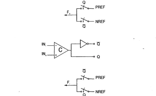
The DAC is useful for several reasons. The first is that the DAC serves to buffer the output of the modulator from the summing nodes of the integrators. Since the output is fed back to multiple nodes in the system, a voltage buffer is necessary to avoid loading the output. Second, the DAC can scale the output voltage to the appropriate levels. This ability is not particularly useful, since our capacitor ratios can be altered to provide the correct scaling. Lastly, proper design of the DAC helps preserve the AC gain stability of the modulator. Even if the output was able to drive large capacitive loads, it would still not be prudent to simply connect the output directly to the summing nodes, because doing so results in large variations in AC gain.
In order to maintain AC gain stability, the charge fed back to the integrators must be consistent for a given quantization error signal; that is to say, f[n] must be stable (either OV or 5V for a given "n"). Since the quantizer is simply a comparator with a D flip-flop on the output, the analog output voltage level is dependent on the supply (VCC) that powers it. Over time, a digital "1" can change from 4.75V to 5.25V, depending on temperature and other external factors. So while a digital "0" would correspond to OV, a digital "1" can vary over a large range of analog voltages. Such inconsistencies in the feedback signal will cause variations in the AC gain of the modulator.
In this system, the 1-bit DAC is implemented as shown in Figure 2-18. The digital output of the modulator is used as a control signal to switch F+ and F_ between the stable reference voltages PREF and NREF (for this ASIC, PREF=4.25V and NREF=OV). These reference voltages source enough current to drive the integrators' input capacitors and vary less than .35% over the full range of temperature and process variations. This design is necessary to stabilize the AC gain of the modulator.
Understanding the operation of the switched-capacitor integrator (as well as its limitations) is crucial to understanding the advantage of a CT implementation. We have already seen that the thermal noise generated by the input capacitors is the limiting factor in the achievable resolution of this modulator. The next chapter will
0 PREF F. NREF IN.
-C
IN,, + PREF F. NREF 0Figure 2-18: 1-bit feedback DAC as it is implemented in the existing third order modulator design
reveal further weaknesses and suggest a CT topology as a solution. Furthermore, we shall see that when it comes time for us to design a CT modulator, the 1-bit DAC will require extensive redesign.
Chapter 3
Advantages and Disadvantages of
Continuous-Time E-A Modulators
In the previous chapter, a third-order discrete-time (DT) modulator was pre-sented. The major performance limitation is due to the high level of thermal noise at the input of the modulator. It is believed that a continuous-time (CT) modulator topology may eliminate this problem. A fair amount of research has been done on CT topologies, as they are potentially useful in minimizing power dissipation, silicon area, and thermal noise.
While there are many benefits to be had from this implementation, there are several significant drawbacks which make such a topology unpopular, especially for design on silicon. The following chapter presents research done on CT modulator topologies and investigates its viability for our specific application.
3.1
Benefits
In redesigning the third-order modulator from the previous chapter, we are defi-nitely interested in reducing the thermal noise floor at the input, but other areas of interest include reducing power dissipation and area on chip. Since ultimately, several of these A/D converters may be needed for "system-on-chip" designs, it is worthwhile to target these areas when redesigning.
F
Cf
R
VIN-A
VOUT+ VIN+A
VOUT-Ri
Rf
FCf
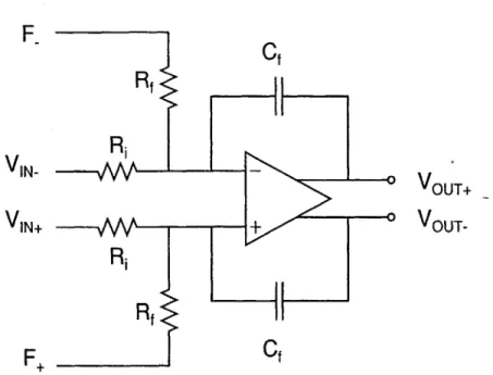
Figure 3-1: A simple continuous-time integrator (fully-differential)
One of the major building blocks of our E-A modulator is the integrator, which we have seen implemented in discrete time using switched-capacitor techniques (Figure 2-17). A simple CT integrator can be implemented as shown in Figure 3-1.
3.1.1
Reducing power consumption
The desire for increasingly better digitizers continues to grow, and more often than not, the solution is to design higher order E-A modulators. Much work has been done in obtaining methods to stabilize such designs; however, another drawback of high order modulators exists: increased power consumption. Adding another switched-capacitor integrator (and thus another opamp) to a modulator design requires the use of a significant amount of additional power.
Switched-capacitor integrators require a large amount of current in order to func-tion normally. This trait is due to the fact that the output must be able to settle quickly when driving capacitive loads: the feedback capacitor (Cf) and the input capacitance of the successive integrator. It is imperative that the outputs not be slew-rate limited, since studies have shown that it can cause an increase in harmonic
slew-rate limiting at the input, oversampled system like E-A modulators are not, because the input changes slowly with respect to the sampling clock. However, E-A mod-ulators can often have slew-rate limiting problems inside the loop at the integrator outputs.
Furthermore, the integrator output must settle to its final value prior to the next switching cycle; otherwise, a gain error will be introduced into the modula-tor, which can further degrade SNR. At low sampling frequencies, this error may be easily avoided, but for high-resolution E-A modulators, it is most likely that the oversampling ratio will be as large as possible, resulting in a short amount of time between clock phases. With such a small amount of time to charge these load capac-itances, the switched-capacitor opamps must be designed so that the output stage is capable of supplying large currents, thus avoiding long settling times or slew-rate limiting. The use of large currents translates into using high-power opamps for E-A modulator design.
CT modulators can more easily avoid the slew-rate problem. The main reason is that the load capacitance seen at the integrator outputs can more easily be minimized when using CT integrators. Therefore, the integrator opamps can be designed to
supply less current to the output in order to avoid slew-rate limiting. Moreover, the bandwidth requirement of the opamps is reduced; designing opamps with less bandwidth can also reduce power consumption. The extent to which power can be saved is still dependent on the capacitances seen at the output node, but the opamp design constraints are now more relaxed. Qualitatively, we can see that the power consumption can be reduced from our original DT design-we will hopefully get a better feel of the quantitative reduction once we design a comparable CT E-A modulator.
3.1.2
Decreasing chip area
There are two major characteristics of CT modulators that decrease the amount of real estate required on chip. The first involves the need for an anti-aliasing filter in DT systems. In order to avoid high frequency noise from aliasing into the band of interest
(and reducing the SNR), an anti-aliasing filter must be placed before the analog signal is sampled. Since DT modulators inherently sample (and hold) when using switched-capacitors, the filter must be placed before the modulator input. However, CT modulators sample the signal inside the modulator loop, prior to the quantizer. In this type of design, the modulator loop inherently provides anti-aliasing!
The Nyquist criterion tells us that if we sample a signal at a frequency of
f,,
anytwo tones that differ in frequency by a multiple of f, overlap in the spectral plot; that is, they are indistinguishable. Our band of interest is nominally 20kHz; hence,
any spectral component (more specifically, noise) at
f,
+ 20kHz will be appear at20kHz, thus adding more noise power in the signal band! Anti-aliasing filters remedy this problem by lowpass filtering the signal before sampling, thus attenuating any high-frequency noise which may alias into the signal band.
Examining the block diagram of Figure 3-2, we can see that where the signal is sampled has some importance with respect to aliasing. If the signal is sampled at, point "A" (prior to the input), then an anti-aliasing filter is needed to attenuate the high frequency noise. However, if the sampling is done at point "B" (as in CT designs), then the first three integrator stages act as an anti-aliasing filter! The transfer function from point A to point B should resemble a third-order low-pass filter, giving us roughly 60dB of attenuation at the sampling frequency (assuming
each integrator has a crossover frequency one decade below
f,
in order to stabilizethe loop). Thus, higher-order CT modulator designs provide increasingly better anti-aliasing.
The second characteristic which allows us to reduce chip area is evident in the circuit requirements of the switched-capacitor and CT integrator. Making resistors in silicon requires much less space than making capacitors. Hence, we can realize integrators with larger gains and bandwidths using less silicon area. This fact is easy to see if we examine the transfer function for the CT integrator shown in Figure 3-1.
1 -R
A a1 a2 a3 + f + f +
f
yn] C3 b1 b2 b3] DAC-Figure 3-2: Block diagram of third order EA circuit.Smaller resistors and capacitors result in larger gains, whereas in the switched-capacitor case, the integrator characteristics are determined mainly by the ratio be-tween two capacitors (see Equation 2.18). It should be obvious that a CT integrator can use the minimum sized capacitor for that particular process and vary the resistor size to realize a wide range of gains (minimum and maximum resistor sizes differ by about three orders of magnitude for this particular process). A DT integrator's gain has a much greater effect on its size (assuming the sampling frequency cannot be varied). This effect relaxes the area constraints on our modulator designs, allowing smaller designs to achieve similar resolutions.
Another way CT modulators can become more compact is that certain physical devices behave as CT integrators (some accelerometers and fluxgate magnetic sensors are examples [1]). There exist certain circuit designs which use the physical char-acteristics of these devices to implement the first stage of a E-A modulator, thus eliminating the space needed for a circuit implementation of the first stage. While this technique is not relevant to this design, it is an interesting one nonetheless.
3.1.3 Lowering thermal noise
important. The major reason for this assertion is that any circuit non-linearities or noise sources in the later stages of the modulator are divided by the gain of the first stage when those errors are input-referred. Thus, any precise circuit requirements needed to minimize such non-linearities can be relaxed in the second and third stages of the modulator, even though the first stage necessitates excruciating attention to detail.
This feature is especially relevant when discussing circuit noise. The main circuit noise sources are those at the first stage. The main noise sources include those from opamps and from components such as switches, capacitors, and resistors. Opamp noise is generated by the MOSFET transistor pair in the opamp's differential input stage. There are two types of noise generated by MOSFETs: flicker noise (or 1/f noise) and thermal noise. Flicker noise is small at higher frequencies, but can have a substantial effect at low frequencies. The voltage noise appears at the gate, and it's
noise power is given by [2]:
K
VWL) gl = WLCaxf (3.2)
The term K (not to be confused with Boltzmann's constant) is a value dependent on device characteristics. Since flicker noise is inversely proportional to the area of the MOSFET, we need only to increase the device sizes of the appropriate transistors. The MOSFET's thermal noise is generated by the resistive channel of the MOSFET in the active region. Although current noise is generated in the channel, it translates to voltage noise at the gate. The noise power at the gate due to thermal noise is calculated to be [2]:
S(f) 8kT (3.3)
3gm
In this case, the "k" is Boltzmann's constant (1.38 x 10 2 3 JK-1) and T is absolute
temperature. Combatting this noise is a simple matter of increasing the transcon-ductance (gm), which can be done by increasing the device size as well as increasing the bias current. When designing opamps, the input stage is often biased at higher
currents than subsequent stages for the purpose of minimizing thermal noise; the tradeoff is increased power consumption.
These noise sources are present in both DT and CT modulators. However, the noise generated from components are significantly different. We will discuss the DT case first. Examining the switched-capacitor integrator again (Figure 2-17), we see that the only components at the input are capacitors and switches. The switches are implemented with MOSFETs; subsequently, the modulator input is mainly affected by the thermal noise generated in the channel. This noise is small compared to the capacitor noise. While capacitors do not generate noise of their own, they do accumulate noise from other sources. In this case, noise is accumulated from the switches. It has been shown that capacitor noise power is independent of the noise power from other sources and is given by Equation 3.4. Note that since this capacitor is sampled by a switch, the capacitor noise will be slightly larger than this value due to aliasing. Nevertheless, it is still a good estimate of the thermal noise.
v2) CU = (3.4)
=C
On-chip capacitors tend to be small (on the order of picofarads), thus the noise generated tends to be high. Furthermore, since switched-capacitor integrators contain a feedback capacitor (Cf) and an input capacitor (Ci), there are two sources of this thermal noise. Thus, when choosing capacitor sizes, the designer must trade off between component area and thermal noise level.
CT modulator designs use input resistors, feedback capacitors, and no switches to implement the integrators. So while the noise generated from the single feedback capacitor still exists, the noise from the input capacitor is absent. Instead, the input resistor (Ri) generates noise with a noise power of:
V(f) = 4kTR (3.5)
In comparison to the capacitor noise, this value is significantly smaller when con-sidering that on-chip capacitors are usually tens of picofarads (10-11) while on-chip
resistors are usually tens of kiloohms (10). It is easy to see that when dealing with components of these sizes, CT integrators generate less noise than their DT counter-parts.
3.2
Drawbacks
Although CT modulators seem well suited to solve the problem of a small, low-power, high-resolution A/D converter, they are not without their difficulties. Indeed, it is these complications that prevent CT topologies from gaining more widespread use. Such problems with CT modulators include poor absolute component tolerances, data-dependency in the feedback DAC, and clock jitter. However, the previous section should convince any E-A modulator designer that if these issues could be overcome, CT architectures would be an extremely powerful solution to the increased demands for low power E-A conversion.
3.2.1
Absolute component tolerances
In section 2.2.2, we saw that one of the more useful characteristics of switched-capacitor filters on a silicon process was that the frequency response was solely based on component ratios, which are well-controlled on silicon. Moreover, the frequency response is dependent on the sampling frequency, which is beneficial in this case, because the band of interest depends on the sampling clock as well. However, the transfer function of the CT integrator of Figure 3-1 relies on the value of the the time constant RC.
Unfortunately, since the poles and zeroes of the system are now determined by RC time constants, we can no longer accurately place poles and zeroes as in a switched-capacitor circuit. The IC process used for this project specifies the absolute tolerance of high-poly resistors to be t20% and the temperature coefficient to be -1446ppm/oC. Furthermore, the absolute tolerance of capacitors is +8%, with a temperature
coeffi-cient of -25ppm/0 C. As if these problems were not difficult enough to deal with, an
15kHz-25kHz, depending on physical device characteristics. Considering this frequency vari-ation and the poor absolute tolerances of these on-chip components, it becomes clear that any CT modulator design for this application must be tolerant to large errors in pole and zero placement.
3.2.2
Sample-and-hold circuit
Another small annoyance of this topology is the need for a sample-and-hold circuit. Switched-capacitor modulators inherently sample and hold, thus eliminating the need to design one. For this topology, a separate sample-and-hold must be designed and implemented in front of the quantizer. This requirement results in increased silicon area. However, we have seen that CT modulators eliminate the need for anti-aliasing filters; considering the effectiveness of using the integrator stages for a filter, the added nuisance of a sample-and-hold is trivial, as is the area requirement. We will see later on that our particular design constraints for this SHA are extremely loose, and as a result, the area requirement is nearly inconsequential.
3.2.3
Return-to-zero DAC
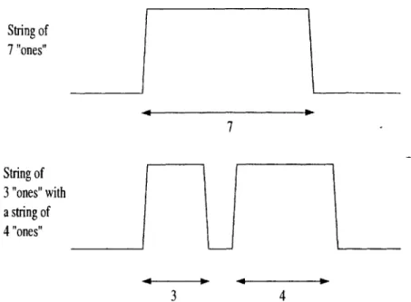
The 1-bit D/A converter in the feedback path of the modulator is usually used to buffer and sometimes scale the output bitstream before feeding it back to the input. In a CT modulator, the design of this DAC becomes significantly more complicated, because a data dependency occurs when the output signal levels are directly fed back to the input [5]. Each bit transition requires a small amount of time to settle; so the energy of the pulse for a long string of "I's" is not the same as the series of pulses containing the same number of "l's." Figure 3-3 illustrates this concept.
A data dependency results because for an output with a high density of "ones," more energy is fed back to the input than for an output with equal density of "ones" and "zeroes." Therefore, the system characteristics change slightly depending on the input. This energy fluctuation is not a concern in DT modulators, because the DAC is controlled by the sampling clock and is implemented in such a way that the output
String of 7 "ones" 7 String of 3 "ones" with a string of 4 "ones" 3 4
Figure 3-3: Two waveforms with 7 "ones." Due to rise and fall times, the energy (area under the curve) in the first waveform is slightly different than the energy in the second.
voltage levels are fed back to the input after settling.
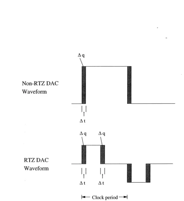
We can rectify the situation by implementing a "return-to-zero" D/A converter in
the feedback path. Such a device generates one pulse for every sampling period; thus, the energy fed back to the input is the same for every "one." Therefore, the energy of the signal in the feedback path is independent of the data. The return-to-zero waveform is illustrated in Figure 3-4.
There are other minor complications which arise from using RTZ DACs. We will discuss these further when it comes time to design a CT modulator of our own.
3.2.4
Clock Jitter
Perhaps the most problematic complication arising from the use of CT modulators is that of clock jitter. Any phase noise present in the sampling clock is very easily introduced into the modulator as a large noise source. Why are CT modulators more susceptible to this kind of error than DT modulators? Figure 3-5 helps to illustrate why [1]. The At term is the clock edge's time error due to jitter. The gray-shaded
- - ----.
-Ideal Output
Actual Output
Waveform of a Return to Zero DAC
1 sampling period
Figure 3-4: Waveform of a Return-to-Zero DAC.
Discrete-Time Continuous-Time
At
At
Figure 3-5: Feedback current waveforms for a single sampling period
CT modulators, this amount is very large. One can think of Aq as representing the error signal fed back to be corrected.
For DT modulators, the output voltage is sampled, then used to charge the input capacitors of the first integrator stage. Hence, most of the current usually discharges into the capacitor at the beginning of the clock period; any jitter in the sampling clock results in a negligible error. However, CT modulators supply current to the input resistors of the first integrator stage for the duration of the pulse. Clock jitter is troublesome in this case, as quite a bit more energy is fed back to the input with this kind of feedback waveform. The result is that a fair amount of random error (noise) is introduced at the modulator input. This noise can degrade SNR, especially
![Figure 2-7: Spectral Density of y[n]. All the out-of-band noise has been filtered out.](https://thumb-eu.123doks.com/thumbv2/123doknet/14472475.522574/27.918.193.788.120.334/figure-spectral-density-y-n-band-noise-filtered.webp)