A Continuous-Time Multi-Stage Noise-Shaping
Delta-Sigma Modulator with Analog Delay
ARCHIVES
by
Do Yeon Yoon
MASSACHUSETTS INSTITUTE OF TECHNOLOGY
JUL
0
1 2012
B.S., Electrical Engineering
LIBRARIES
Korea Advanced Institute of Science and Technology (2010)
Submitted to the Department of Electrical Engineering
in partial fulfillment of the requirements for the degree of
Master of Science in Computer Science and Engineering
at the
MASSACHUSETTS INSTITUTE OF TECHNOLOGY
June 2012
©
Massachusetts Institute of Technology 2012. All rights reserved.
Author ... ...
Department of Electrical Engineering
May 22, 2012
Certified by...
Hae-Seung Lee
Professor
Thesis Supervisor
n
Accepted by ...
Llil
A. Kolodziejski
Professor
Chair, Department Committee on Graduate Students
A Continuous-Time Multi-Stage Noise-Shaping Delta-Sigma
Modulator with Analog Delay
by
Do Yeon Yoon
Submitted to the Department of Electrical Engineering on May 22, 2012, in partial fulfillment of the
requirements for the degree of
Master of Science in Computer Science and Engineering
Abstract
A new continuous-time multi-stage noise-shaping delta-sigma modulator has been
designed. This modulator provides high resolution and robust stability characteris-tics which are the primary advantages of the conventional multi-stage noise-shaping architecture. At the same time, previous critical challenges that degraded the over-all performance of multi-stage noise-shaping delta-sigma modulators are eliminated through several unique techniques. Additionally, these techniques relax the require-ments of each component of the proposed delta-sigma modulator. As a result, this new delta-sigma modulator architecture can provide several advantages that are not obtainable in other modulator architectures.
Thesis Supervisor: Hae-Seung Lee Title: Professor
Acknowledgments
Since I started a new journey to the Ph.D. at MIT, I have encountered many people that have helped me in completing my research.
First and foremost, I would like to heartily thank my advisor, Professor Hae-Seung Lee. I have always been inspired by his extensive knowledge and creative insight in the area of analog circuit design. Moreover, his caring guidance has fully encouraged me to move toward the right direction. It has been a huge honor to work with him.
I would like to thank Jeffrey Gealow, Paul Ferguson and many other people at
MediaTeK, who suggested the interesting research topic I am working on, and keep helping me in different ways for my research. Especially, Jeffrey has been always willing to answer my questions and help me to fully understand delta-sigma data converters.
I would like to thank all the lab mates in Professor Lee's group: Albert, Daniel,
Jack, Sunghyuk, Mariana, Miguel, Sabino, and Xi. I could freely discuss and learn about many issues in my area with them, when doing my own research. Not only that, but I could also rely on these friends, whenever I needed some help for any kinds of problems.
I would also like to express my appreciation to all my colleagues in my office:
David, Eric, Grant, Kailiang, Philip, and Sungwon. My life at MIT could have been harsher without their help. They always make me feel relaxed.
Last but not least, I would like to thank my family. My father and mother have always given me unconditional love, which I have completely depended on. I would also like to thank my sister for her full support. I could never have come this far without them.
Contents
1 Introduction
1.1 M otivation . . . . 1.2 Thesis Organization. ...
2 Overview of a AE ADC
2.1 Oversampling and Noise Shaping ...
2.1.1 Oversampling ...
2.1.2 Noise Shaping ...
2.2 Overall Structure of a DT AE ADC . . . .
2.3 CT AE ADC . . . .
2.3.1 Difference between DT and CT AE
2.3.2 CT AE Modulator Implementation
2.3.3 CT AE Modulator Issues . . . . .
3 Multi-Stage Noise-Shaping AE Modulator 3.1 Block Diagram . . . .
3.2 NTF of a MASH AE Modulator . . . . .
3.3 CT MASH AE Modulator . . . .
3.4 Previous Work . . . .
Modulators
4 A New CT MASH AE Modulator
4.1 DT Sturdy-MASH AE Modulator ...
4.2 Main Challenges and Solutions of a CT MASH AE Modulator ...
15 16 19 21 21 23 24 28 28 29 30 32 35 35 38 40 42 45 45 48
4.2.1 First Solution: Feedforward Path in the 2"d-Stage . . . . 50
4.2.2 Second Solution: Analog Delay . . . . 53
4.3 Overall Implementation . . . . 58
5 Simulation Results 61 5.1 SQNR Comparison . . . . 61
5.2 Stability Issue . . . . 63
5.3 Finite DC Gain and UGBW . . . . 65
5.4 Acceptable Input Range . . . . 68
6 Conclusions 71 6.1 Thesis Summary . . . . 71
List of Figures
1-1 DR and signal bandwidth requirements of ADCs for different wireless applications . . . . 1-2 DR and signal bandwidth of different types of ADCs . . . .
1-3 FOM and signal bandwidth of different types of ADCs . . . .
2-1 Analog-to-digital conversion . . . . 2-2 4-level quantizer characteristics: (a) transfer curve, (b) error function,
(c) probability density function . . . .
2-3 2-4 2-5 2-6 2-7 2-8
Attenuated in-band noise . . . . Linear model of AE ADCs . . . . Shaped in-band noise . . . . Block diagram of a DT AE ADC . . .
Block diagram of a CT AE ADC . . .
Impulse response comparison: (a) DT matched impulse response . . . .
16 17 17 21 22 . . . . 23 . . . . 24 . . . . 27 . . . . 28 . . . . 29 loop filter and CT path, (b)
3-1 n-stage MASH AE modulator . . . . . 3-2 2-stage DT MASH AE modulator . . .
3-3 NTF graphs of an original 4th-order AE modulator and a MASH
3rd+1st-order AE modulator: (a) overall NTF, (b) NTF within the in-band frequency . . . .
3-4 NTF graphs of an original 4th -order AE modulator and a MASH 3rd+1st-order AE modulator: (a) NTF with a 4-bit quantizer, (b) NTF with a 4-bit quantizer and gain blocks . . . .
31 36 36 38 39 . . . . . .
3-5 Block diagram of a CT 2-stage MASH AE modulator: (a) block
dia-gram, (b) output of a quantizer and a delay block . . . .
Block diagram of a sturdy-MASH AE modulator . . . .
Block diagram of an early version of the new CT-MASH AE modulator Loop filter in the 2nd-stage . . . .
SQNR from the proposed AE modulator and others . . . .
4-5 Signals at the input and output of the delay block: (a) block diagram,
4-6 4-7 4-8 4-9 4-10 5-1
(b) signals from the ideal DT delay block,
block . . . . Analog delay implementation with an LPF Transconductor with a built-in LPF . . . .
Block diagram of the final architecture . . 2nd-stage implementation . . . .
Overall schematic . . . .
SQNR comparison . . . .
(c) signals from alternate
. . . . 54 . . . . 55 . . . . 56 . . . . 57 . . . . 58 . . . . 59
5-2 Out-of-band average noise floor comparison
5-3 Input and output of the LPF: (a) Hinf=1.5, (b) Hinf=2.0, (c) Hinf=2.5
5-4 SQNR graphs based on different finite DC gains and UGBWs: (a) pro-posed CT MASH AE modulator with the gain-of-1 block, the feedfor-ward path, and the LPF, (b) original CT MASH AE modulator with the gain-of-1 block, the feedforward path, and the LPF, (c) original 3 d -order AE modulator . . . .
5-5 SQNR graphs based on different finite DC gains and UGBWs. (a)
Gain-of-4, (b) Gain-of-i . . . . 5-6 SQNR graphs based on different finite DC gains and UGBWs: (a)
Gain-of-4, (b) Gain-of-4 with the gain-enhancement 1S"-integrator . .
5-7 SQNR vs. input amplitude . . . . 62 63 64 65 66 67 68 4-1 4-2 4-3 4-4 40 46 48 50 53 . . . .
5-8 Signals when the input amplitude is 110% FS: (a) input of the entire
modulator, (b) output of the quantizer in the 1s"-stage, (c) input of the 2nd-stage, (d) output of the entire modulator . . . . 69
List of Tables
Chapter 1
Introduction
Most electronic systems receive analog signals from the real world and then convert them to digital signals for processing in the digital domain. Therefore, analog-to-digital converters (ADCs) are essential in many electronic systems. In particular, modern wireless communication applications require accurate and high-speed ADCs. Such ADCs must consume low power due to the significant constraints in battery-powered wireless systems (e.g., mobile phones). For wireless applications, delta-sigma
(AE) ADCs have been used for fifty years, since the first idea of AE operation
was presented [1], and this idea was adapted to the real ADC [2]. Among other types of ADCs, AE ADCs are suitable for modern wireless applications, due to their oversampling, high dynamic range (DR), and low-power consumption characteristics. Over the last decade, significant efforts have been made to increase the speed of the AE ADCs with high resolution and low-power consumption. As a result, many architectures for AE ADCs have been investigated, but they have been unable to achieve performance metrics required for next generation wireless applications. For this reason, this thesis presents a new AE ADC architecture that can achieve the higher resolution and signal bandwidth required by modern wireless applications.
1.1
Motivation
Wireless communication is a rapidly advancing field and new wireless applications are continuously being developed.
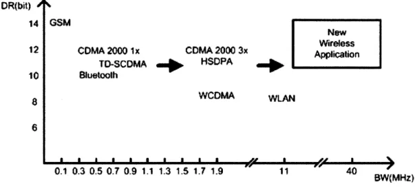
DR(bit)
14 GSM
New
12 CDMA 2000 1x CDMA 2000 3x Wireless
TD-SCDMA HSOPA
10 Bluetooth
8 WCDMA WLAN
6
0.1 0.3 0.5 0.7 0.9 1.1 1.3 1.5 1.7 1.9 11 40 BW(MHz)
Figure 1-1: DR and signal bandwidth requirements of ADCs for different wireless
applications
Figure 1-1 shows each application space and the required DR [3]. As shown in Figure 1-1, new wireless applications, such as Long Term Evolution technology, demand signal bandwidth and resolution over 50-MHz and 14 bits, respectively. At
the same time, the systems for new wireless applications must consume low power due to the limited battery-power. In order to meet all these requirements, a proper
type of ADCs has to be carefully chosen.
Figure 1-2 shows the DR and signal bandwidth of ADCs presented at the Inter-national Solid-State Circuits Conference and Symposium on VLSI circuits from 1997 to 2012 [4]. As shown in the figure, to achieve a DR over 70-dB, AE and pipelined ADC architectures are typically used. Especially, the achieved DR values of AE ADCs are higher in this region. When considering power consumption by using the Figure-of-Merit (FOM) as shown in Figure 1-3 [4], it is shown that AE ADCs have better advantages. Equation 1.1 shows how FOM can be calculated.
* CT tke gma E DT Deta-Sigma A Pipeline x SAR ----_ _ -- iFlash * Folding A Two-Step A 120 -110 -10D - 90- 80-70 60- so-40 30-20 1E+03 A 1E+10 1E+11
Figure 1-2: DR and signal bandwidth of different types of ADCs
*CT Delta-Sigma _ DT De Ita-Sigma A Pipe line X SAR A * Flash 0 Folding + Two-Step
1E+04 1E+05 1E+06 1E+07
Signal Bandwidth ("z)
1E+08 1E+09 1E+10 1E+11
Figure 1-3: FOM and signal bandwidth of different types of ADCs
a
1E+04 1E+OS 1E+06 1E+07 ZE+08 IE+09
Signal Bandwidth tH4 1.90E+02 -1.80E+02 -1.70E+02 -1.60E+02 -1.50E+02 140E+02 -1.30E+02 -1.20E+02 -1.1OE+02 -1.OE+02 -1E+03
BW
FOM = DRdB + 10 log(
)
(1.1)P
where P is power and BW is signal bandwidth. The higher FOM, the more power-efficient ADCs. For signal bandwidth near 20-MHz, the FOM of AE ADCs is generally high, while achieving the high DR. Therefore, AE ADCs are a suitable architecture for use in upcoming wireless applications.
ADCs can be implemented in either a discrete-time (DT) or continuous-time (CT) structure. Until recently, the majority of AE ADCs have been implemented in DT by using switched-capacitor(SC) techniques. Since the implementation methodologies of DT AE ADCs have been thoroughly examined, it is much easier to build AE ADCs in DT. Moreover, due to the robustness of the capacitor matching in a modern
CMOS process, DT AE ADCs can easily provide high resolution. However, since next
generation wireless applications require high speeds of operation, a renewed interest in CT AE ADCs is observed, as they are able to work at much higher sampling frequencies than comparable DT AE ADCs. The detailed advantages of CT AE
ADCs will be described in the following chapter.
For these reasons, this thesis presents a new CT AE modulator architecture, which is the primary component of a CT AE ADC, to achieve high resolution and signal bandwidth, while consuming low power. This new architecture is designed specifically for the application of multiple-input multiple-output wireless receivers. The main goal is to achieve a 50-MHz signal bandwidth and DR 84-dB or greater, while keeping power consumption below 100-mW. Achieving this goal will solve many of the problems found in current CT AE modulator designs. The fundamental idea is to implement a CT multi-stage noise-shaping (MASH) AE modulator consisting of two stages. This structure will give additional noise suppression without introducing stability and complexity issues and will mitigate accuracy requirements of the analog loop filter at high sampling frequencies.
1.2
Thesis Organization
A new CT MASH AE modulator is proposed in this thesis. First, several common
issues of CT AE modulators are presented. These issues extend to challenges in the design of an original CT MASH AE modulator. Finally, these issues are resolved by use of a new CT MASH AE modulator. Several unique advantages of the new CT
MASH AE modulator are also presented. The thesis is organized as follows:
Chapter 2 describes the fundamentals of AE ADCs. CT AE ADCs are studied primarily to help motivate the rest of the thesis. The several issues that arise when a DT AE modulator is converted to a CT AE modulator are described as well.
Chapter 3 provides an explanation of MASH AE modulators, and, in particular, describes the bottlenecks of a CT MASH AE modulator.
Chapter 4 proposes a new CT MASH AE modulator based on the DT
sturdy-MASH AE modulator. In this chapter, solutions to several challenges in the design of
conventional CT MASH AE modulators are presented. The practical implementation of this architecture is also proposed.
Chapter 5 presents the simulation results from the proposed CT MASH AE mod-ulator. Compared to other CT AE modulators, distinct advantages of the new archi-tecture are proven based on the simulation results.
Chapter 2
Overview of a AE ADC
This chapter provides fundamental information about AE ADCs. First, oversampling and noise shaping characteristics are described. Based on these characteristics, the overall structure of AE ADCs is illustrated with operational descriptions. Moreover, differences between DT and CT AE ADCs are described, and the main advantages and issues of CT AE ADCs are presented to aid in understanding the rest of the thesis.
2.1
Oversampling and Noise Shaping
AE ADCs exploit two primary characteristics: oversampling and noise shaping. These
two characteristics can be explained by fundamental analog-to-digital conversion.
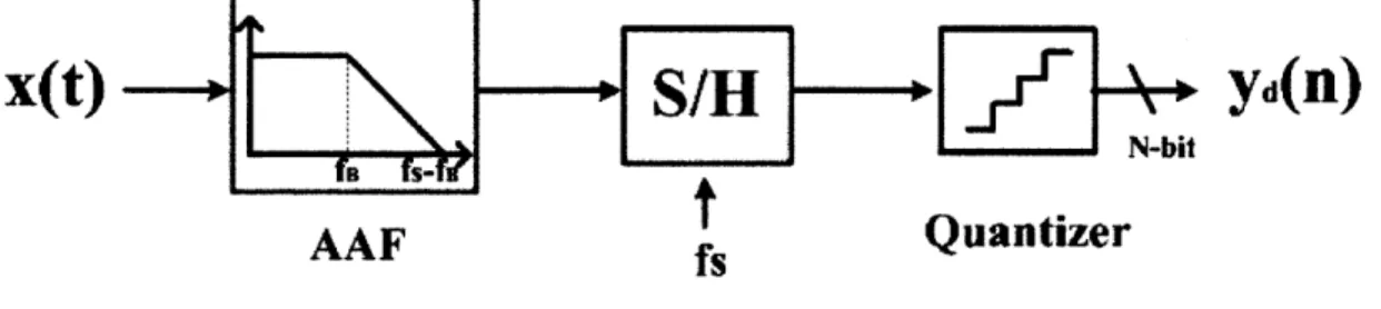
x(t)
yd(n)
AAF
fs
Quantizer
Figure 2-1: Analog-to-digital conversion
conversion is to sample a CT signal, by using a sample-and-hold(SH) block, and then to assign the sampled value to one of discrete reference values, which is commonly referred to as quantization. Prior to sampling, an anti-aliasing filter(AAF) is needed to avoid high frequency components from folding into the signal bandwidth.
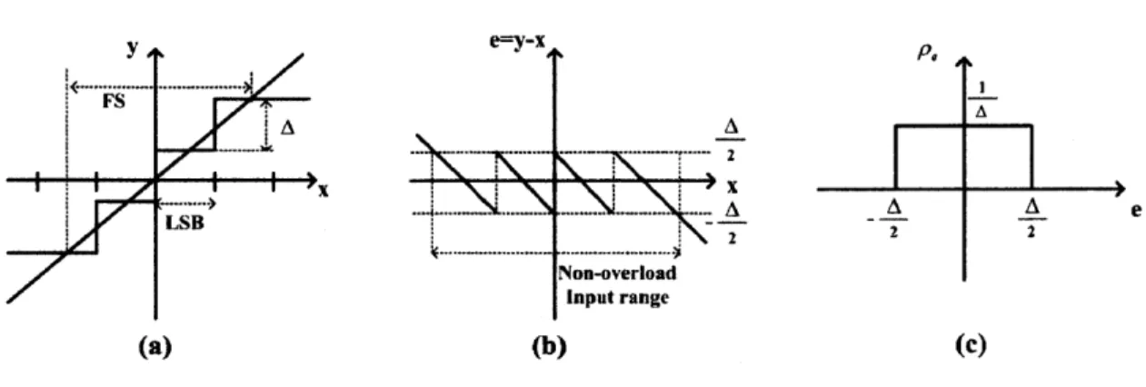
Y t ~e=y-x tA1 A Non-overload input range A A e 2 2 (a) (b) (C)
Figure 2-2: 4-level quantizer characteristics: (a) transfer curve, (b) error function, (c)
probability density function
The transfer curve of an example 4-level quantizer conversion is shown in Fig-ure 2-2(a). The least-significant bit (LSB) represents the difference between input thresholds and the quantizer step size is shown as A. These two values are equivalent in the sample system and are given by A - LSB - FS/3, where full-scale(FS) is the
maximum input range. In general, for an nbit quantizer, the step size becomes A
-FS/(2n-1). Compared to the ideal case y = x, the quantization error, e, can be found and is illustrated in Figure 2-2(b). Within the non-overload input range, given by
[-FS/2-LSB/2, FS/2+LSB/2], the quantization noise, e, is distributed within the range [-A, A]. As shown in Figure 2-2(b), the quantization error is directly determined by the input, but under certain circumstances [5] [6] [7] [8], it can be modeled as white noise that is uniformly distributed in the range [-A/2, A/2], as shown in Figure 2-2(c). Based on this probability density function, the total quantization noise power, o can be calculated. Since quantization noise power is also uniformly distributed in the range [-fs/2, fs/2], the power spectral density of the quantization noise is given by:
1
2i 21 A2 __f=-I e del (2.1)
fs fs [A J /2 12
fs
Within the in-band frequency range, the quantization noise power is given by
I
fB
PE
-f B
SEf)df 2fBA 2
12fs (2.2)
where fB represents the signal bandwidth.
2.1.1
Oversampling
According to the Nyquist Theorem, the sampling frequency, fs, should be greater than
twice fB. Therefore, the minimum sampling frequency is 2fB, commonly referred
as the Nyquist rate. The Nyquist rate is the sampling frequency used by Nyquist ADCs. Unlike Nyquist ADCs, oversampling ADCs such as ATE ADCs use a sampling frequency that is much higher than 2fB. In this case, the oversampling ratio (OSR)
is defined as OSR=fs/2fB. The main advantage of oversampling ADCs is illustrated in Figure 2-3.
PSD
Attenuated
in-band nosie
(PSE)fB
fs/2
Equation 2.2 shows how the in-band quantization noise relates to the oversam-pling characteristic directly. This equation is inversely proportional to the OSR, which means that in-band quantization noise is attenuated, for increased OSR. This is because fixed quantization noise power, o, is uniformly distributed in the range
[-fs/2, fs/2], as shown in Figure 2-3. Therefore, if fs/2 is much greater than fB, the
eventual in-band quantization noise is reduced. Based on Equation 2.2, the in-band quantization noise power can be decreased by the OSR at a rate of 3 dB/octave. This illustrates a simple trade-off between speed and resolution. Another advantage of oversampling ADCs is that the high sampling relaxes the requirements of the AAF, since if fs/2 is much greater than fB, a sharp AAF at the input of a SH circuit is not required.
2.1.2
Noise Shaping
As described previously, high sampling frequency can reduce in-band noise, due to the oversampling characteristic. In addition, AE ADCs have another characteristic, noise shaping, that can further suppress in-band noise. The main idea is that a loop filter in the modulator pushes in-band noise to out-of-band frequencies.
Loop Filter Quantizer Loop Filter
X + H(z)
J
y x + + H(z) ++Yt+
E E
Figure 2-4: Linear model of AE ADCs
Figure 2-4 shows a basic block diagram of DT AE ADCs. It consists of a feedback system with a loop filter, H(z), and a quantizer. The quantization noise, E, is directly injected at the quantizer to create a linear system model. In this case, the output is given by:
1~*
H(z) 1Y =X - () + E- 1(2.3)
1 + H(z) 1I + H(z)
From Equation 2.3, signal transfer function (STF) and noise transfer function
(NTF) can be defined:
H(z) 1
STF H(z) and NTF = (2.4)
1 + H(z) 1 + H(z)
If the loop filter has extremely large gain within the in-band frequency range, STF becomes 1 and NTF becomes 0. Therefore, the input signal, X, passes through
the modulator unaffected, while the quantization noise, E, is suppressed. That is,
E within in-band can be shaped by the NTF. Using this characteristic to make a
low-pass AE ADC, an integrator can be used as the loop filter. On the other hand, to create a band-pass AE ADC, a resonator, which has a large gain at the given center frequency, can be used.
To implement a low-pass AE ADC, the NTF is generally given by:
NTF = (1 - z-1)L (2.5)
where L denotes the order of a loop filter, H(z). To calculate the in-band quantization noise power shaped by the NTF, it is necessary to find the squared magnitude of the
NTF:
NTF(ej") 2 _= 2L |1 - cos(Q) + j sin(Q) 2L (2.6)
= [2 - 2 cos(Q)]L 2 sin(Q)] 2L (2.7)
the output, the squared magnitude of the NTF is multiplied to the quantization noise power. The in-band noise power is given by:
PQ 2 oj
|
NTF(e')|
2dQ =
2
sin( ) dQ (2.8)where QB is defined as QB=7r/OSR. Due to the high sampling frequency, r/OSR is, in general, very small. Within the range [0, -r/OSR], the sine term can be simplified as:
2 .sin - ~ 2. Q (2.9)
2 2
Combining Equations 2.8 and 2.9, the final in-band noise power shaped by the
NTF is given by:
A2 7r/OSR A2
72L
1270 12 (2L + 1)OSR2L+1
Here, compared to using the oversampling characteristic only, the in-band noise power is attenuated more efficiently. This result is illustrated clearly in Figure 2-5. Due to the oversampling characteristic, quantization noise is uniformly distributed over the range [-fs/2, fs/2], so that the in-band noise can be attenuated. The in-band noise is further suppressed by the NTF as shown in Figure 2-5.
The operation of AE ADCs is primarily based on these two characteristics. With a specific OSR, loop filter order, and number of bits of the quantizer, the maximum signal-to-quantization noise ratio (SQNR) can be calculated based on Equation 2.10 as follows:
w2L
SQNRmax = 6.02N + (20L + 10)logiOOSR + 1.76 - 10lo1o 2 L [dB] (2.11)
PSD
....is 2 NTF2 8 8 S 8Shaped
f
in-band nosie
(P)
Figure 2-5: Shaped in-band noise
There are three ways to increase the resolution of AE ADCs: increasing the order of the loop filter, the OSR, and the number of bits of the quantizer. Each method, however, has its own associated costs. First, increasing the order of the loop filter brings about stability issues. Since a AE ADC is a feedback system, if the order of a loop filter is increased (L>2), this system becomes conditionally stable with a limited input range [9]. Second, increasing the OSR gives rise to speed and power problems. Since the actual sampling frequency is limited, simply increasing OSR is an unacceptable solution. Moreover, if higher OSR is chosen, and a high signal bandwidth is required, each block in the AE ADC must consume more power to handle the faster operation speed. Finally, it is not an effective solution to significantly increase the number of bits of the quantizer, since the accuracy of a quantizer is fairly limited. Furthermore, if a bit quantizer is used, non-linearities from the multi-bit digital-to-analog converters (DACs) degrade the linearity of AE ADCs. DAC non-linearities add directly to the input signal and therefore is not suppressed by the NTF. In this situation, increasing the order of a loop filter and then solving the stability issues is a more effective solution. Since increasing the order of the loop filter causes stability problems, alternative methods have been investigated. These
methods attempt to increase the effective order of the NTF, while maintaining a stable lower order loop filter. These methods are presented in following chapters.
2.2
Overall Structure of a DT
AE
ADC
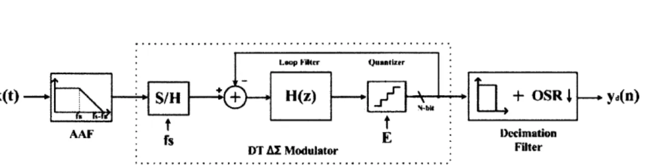
x(t) S/H H(z) + OSR --. yd(n)
AAF s E Dcmation
DT AX Modulator Filter
Figure 2-6: Block diagram of a DT AE ADC
Figure 2-6 shows the overall block diagram of a DT AE ADC. The overall struc-ture of the DT AE ADC consists of an AAF, a DT AE modulator, and a decimation filter. The main characteristic of DT AE ADCs is that the CT signal is sampled at the input of a AE modulator, and the DT signal is processed in the AE modulator. To avoid aliasing when the signal is sampled, an AAF is required before the input of the AE modulator. To implement the desired NTF, a proper loop filter, consisting of switched-capacitor (SC) circuits, is needed. Since the output of a AE modulator is generated at the high sampling frequency, the output data frequency of the AE modulator should be reduced to the Nyquist rate for use in subsequent signal pro-cessing blocks. Therefore, a decimation filter is required at the output of the DT AE modulator, in order to realize a complete DT AE ADC.
2.3
CT
AE
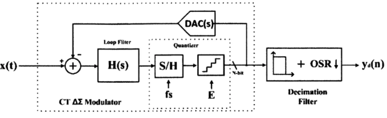
ADC
Figure 2-7 shows the overall block diagram of a CT AE ADC. The main characteristic of CT AZ ADCs is that the input of the CT AE modulator remains a CT signal, until it is sampled at the quantizer. Therefore, the loop filter in a CT AE modulator utilizes
DAC(s
x(t) + + H(s) S/H .+ OSR 4 y(n)
t t
fs E Decimation
CT AX Modulator Filter
Figure 2-7: Block diagram of a CT AE ADC
input signal of a CT AE ADC can be directly fed into the CT AE modulator without an AAF. This is because the sampling process at a quantizer in a loop filter provides an inherent AAF [10]. However, following the CT AE modulator, a decimation filter is still needed. Therefore, CT AE ADCs consist of a CT AE modulator and a decimation filter only. Since an equivalent decimation filter is needed for both DT and CT AE ADCs, only the modulators in AE ADCs will be investigated.
2.3.1
Difference between DT and CT AE Modulators
As mentioned before, the modulators in AE ADCs can be implemented in either a DT or CT structure. The DT AE modulator, based on SC circuits, generally offers higher accuracy compared to that of the CT AE modulator, because this accuracy depends on precise capacitor matching, which is easily achievable by using calibration circuits or dynamic element matching. Moreover, the DT AE modulator is robust under process variation. However, since the DT AE modulator requires op-amp settling within each half-clock period, the gain-bandwidth requirement for the op-amp is rather high, such that the DT AE modulator consumes more power than an equivalent CT AE modulator. Another crucial disadvantage of DT AE modulators is the need for an AAF at its input.
CT AE modulators, however, do not use SCs, so the op-amps require much lower
sampling is performed within the filters, the restriction of maximum sampling fre-quency is dependent only on the regeneration time of the quantizer and the update rate of the DAC [11]. Thus, it is possible for CT AE modulators to function at a higher sampling frequency and achieve wide bandwidth compared to DT AE modu-lators.
Recent wireless applications demand high bandwidth, which decreases the OSR for a fixed sampling frequency, thereby reducing resolution. Thus, to achieve wide bandwidth and maintain high resolution, it is necessary for the AE modulator to work at high sampling frequencies over 1-GHz. To achieve op-amp settling, the unity gain bandwidth (UGBW) of the op-amp in a DT AE modulator must be greater than or equal to about five times the sampling frequency [12]. Therefore, it is extremely difficult for DT AE ADCs to operate at sampling frequencies over 1-GHz. On the other hand, the UGBW of active-RC integrators that CT AE modulators use is the same as the sampling frequencies, or even below, depending on the chosen scaling coefficient [13]. Thus, CT AE modulators are suitable to use for high sampling frequencies to achieve wide signal bandwidth. Moreover, CT AE modulators consume less power while working at high sampling frequencies [14] [15] [16]. In addition, CT
AE modulators can save additional power and circuit complexity due to their inherent
anti-aliasing property. In this regard, CT AE modulators are more suitable to meet the demands of new wireless applications.
2.3.2
CT AE Modulator Implementation
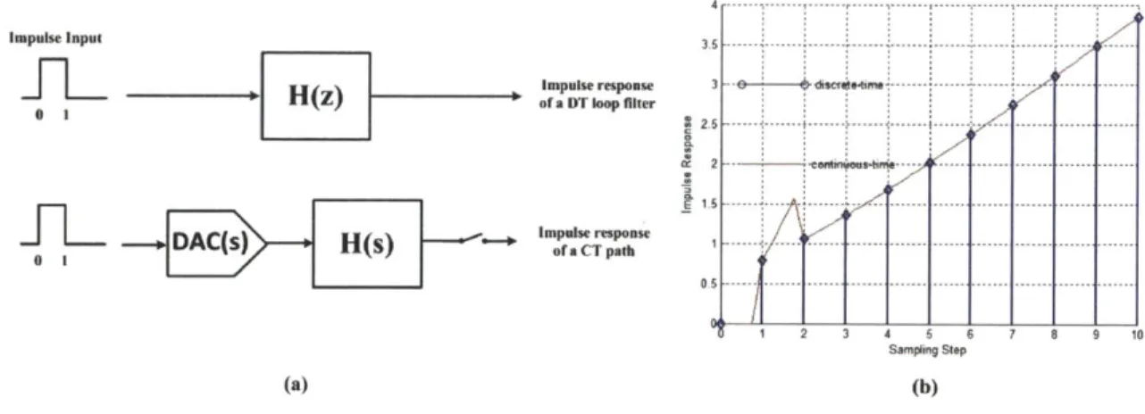
The design methodology of DT AE modulator has been well studied. Additionally, implementation of a DT loop filter is quite straightforward, similar to implementing an active filter by using SC circuits in the z-domain. There are many convenient and useful design tools such as the AE toolbox based on MATLAB [17]. On the other hand, implementing a CT loop filter for a CT AE modulator is more complicated. This is mainly because the CT loop filter can only deal with CT signal input and output, while the target NTF in the design tool is represented by a z-transform in which only a DT signal can be represented. Therefore, the transform conversion
of a loop filter is needed in order for a CT AE modulator to have a same noise shaping characteristic as that of a DT AE modulator. Furthermore, since the output of feedback DACs is a CT signal, DACs are also represented by Laplace-transform, similar to a loop filter, as shown in Figure 2-7.
The fundamental idea in implementing a CT loop filter is to make the CT path, consisting of DACs and a CT loop filter, provide the same result as the output of a DT loop filter at the input of the quantizer at every sampling step. This process can be represented as follows:
H(z) = Z{L--[DAC(s)H(s)][1 6(t - nT,)] (2.12)
n=O
Therefore, with the same digital input, if there is no difference between the output of the DT loop filter and the sampled output of the CT path, which consists of a CT loop filter and DACs. This equivalent CT path can then replace the DT loop filter.
Loop flter pulse/imnplse responses (negated)
Impulse Input 3 4Sap S- 7 .
Figure ____2.-8:' Impulse response sn3a DT loop tefitmeradC pth(b
matchedImpulse response
froH a) lo pathfilter
0 1
75
( 2 3I S67 10 Sampling Step
(a) (b)
Figure 2-8: Impulse response comparison: (a) DT loop filter and CT path, (b) matched impulse response
A practical way to implement a CT loop filter is shown in Figure 2-8(a). By tuning
the CT loop filter, with the given transfer function of DACs, the impulse response from a DT loop filter and a CT path can be matched. If impulse responses are well matched as shown in Figure 2-8(b) at every sampling step, this CT path shapes the
quantization noise in exactly the same manner as the DT loop filter.
2.3.3
CT AE Modulator Issues
In spite of the several advantages of CT AE modulators, such as fast speed and low power consumption, there are four main issues, especially when high sampling frequencies are exploited: (1) quantizer metastability, (2) excess loop delay (ELD),
(3) multi-bit DAC non-linearity, and (4) clock jitter. The quantizer metastability
issue is due to the variation in comparison time with the input signal [18]. Since the quantizer cannot generate the output instantly, to guarantee the correct outputs form the quantizer, additional delay blocks are needed at the output of quantizer. These delay blocks are simply implemented by latches, which sample the quantizer output delayed by half a clock cycle to allow the quantizer adequate settling time. The second problem is ELD, which is due to the finite transient response of the quantizer and the DAC circuits in the modulator loop filter response [19]. Moreover, the delay that occurs from each integrator due to the finite DC gain and UGBW is also considered as ELD, especially when using high sampling frequencies. ELD introduces additional parasitic poles that increase the order of both the STF and NTF, which make the modulator less stable. To compensate for ELD, several methods have been studied [20]. Among these methods, the best-known technique is to add an additional feedback path from the output of a quantizer to the input of quantizer directly in order to reduce the effect of the parasitic poles [21]. The third issue is DAC non-linearity. In general, a multi-bit DAC consists of several unit-element DACs, based on the number of bits. Ideally, each unit-element DAC is exactly the same, so the output from each unit-element DAC is also precisely matched. The real output value is the sum of all output values from all the unit-element DACs. If there is nonlinearity due to mismatch of unit-element DACs, the output of a multi-bit DAC has a nonlinear error. However, unlike a quantization error, this error cannot be suppressed by the NTF and will be directly reflected at the output of the modulator. Therefore, non-linearity of the unit-element DACs is an important issue. Many techniques have been presented to make accurate multi-bit DACs such as analog calibration [21], digital correction
[22], and dynamic element matching (DEM) [15] [23]. Among them, DEM is one of the most popular techniques. The main idea of DEM is that the thermometer output code from the quantizer is assigned to a different unit-element every time by the DEM circuitry. As a result, the fixed error from the unmatched unit-element DACs can be changed to time-varying error. By switching the assigned unit-element DACs based on the thermometer output code, this error can be modulated out of band. This is a common problem of all AE modulators, but it is much more serious in CT AE modulators, since the matching issue of current-steering DACs is worse than that of
SC DT DACs. Lastly, clock jitter caused by uncertainties in the clock-signal edge
can degrade the resolution of CT AE modulators [16]. In DT AE modulators, DACs move stored charge on the capacitors into the main loop within a sampling period, and this amount of charge is barely affected by the sampling period. Therefore, uncertainties in the clock-signal edge are not significant problems in the DT case. In CT AE modulators, however, since the output of the DACs is current, which is directly synchronized to the sampling period, if the sampling period varies, due to the uncertainties in the clock-signal edge, the amount of charge transferred also varies. Since this error occurs at the output of the DACs, it will be directly observed at the output of the CT AE modulator without suppression by the loop filter. Clock jitter error occurs at the quantizer as well, but is reduced by the loop filter. The clock jitter problem can be attenuated by using a multi-bit quantizer and DAC, since the
Chapter 3
Multi-Stage Noise-Shaping
AE
Modulator
The order of a loop filter is one of the critical factors used to improve the resolution of
AE modulators. However, there is less freedom to increase the order of a loop filter,
because stability compromises signal-to-noise ratio (SNR). Therefore, a large number of architectures have been explored to improve the effective order of the NTF, instead of simply increasing the order of the loop filter. One of best-known architecture is multi-stage noise-shaping (MASH), which can help circumvent this stability issue, while achieving high-order noise shaping [24] [25].
3.1
Block Diagram
Figure 3-1 conceptually shows a MASH AE modulator. A MASH AE modulator consists of several stages. Each stage consists of a stable, relatively low-order AE modulator. The input signal is fed into the 1"-stage, and the quantization noise of the 1st-stage, E1, is extracted. This extracted quantization noise is injected into
the 2nd-stage. The input of each following stage is the quantization noise of the previous stage. Finally, outputs from N stages are digitally filtered, and the real output is generated. This digital filter manipulates outputs from N stages so that all the quantization noise, except for the quantization noise of the last stage, can
X
Filter y
AZ Modulator 3 E2
A Modulator n
Figure 3-1: n-stage MASH AE modulator
be canceled. The quantization noise of the last stage is therefore suppressed by the
order of all the stages in the cascade. Since the AE modulator within each stage has its own feedback and consists of a low-order loop filter, the requirement for the stability of the entire MASH AE modulator is significantly relaxed, even though the final quantization noise is shaped by the high-order NTF.
X
YFigure 3-2: 2-stage DT MASH AE modulator
To examine the MASH AE modulator in more depth, a 2-stage DT MASH ar-chitecture is depicted in Figure 3-2. The input is fed into the 1t-stage, and the quantization noise from the 1"s-stage, E1, is injected into the 2nd-stage. Digital filters
at the quantizer outputs act to cancel Ei and suppress the quantization noise from the 2nd-stage, E2, by the high-order NTF. The overall output is described by:
Y = (STF1 -X + NTF1 -E1) -H1 - (STF2 - E1 + NTF2 -E2)-H2 (3.1)
where STF1 = Hg' , NTF1 - 1 STF2 = H 2zd(Z) and NTF2 = 1+H 1(z)'
In this modulator, if the digital filters are designed as H1 =STF2 and H2=NTF1, E1
is canceled and E2 is shaped by NTF.NTF2. Finally, the output of the example
MASH architecture is represented by:
Y=STF1 -STF2 -X-NTF1 -NTF2 -E2 (3.2)
For an nth-order 1st-stage loop filter and mth-order 2nd-stage loop filter, the quan-tization noise, E2, is effectively suppressed by the n+- -order NTF. However, since
the stability of each stage is determined by the order of its loop filter, the stability of the MASH AE modulator is limited by its highest order loop filter. Since the highest order of the loop filter is still lower than the overall order of the NTF, the MASH AE modulator thus circumvents the stability issue. Therefore, compared to the original
AE modulator with a n + mth-order loop filter, the MASH AE modulator can be
much more stable. Increased stability with high-order noise shaping is the primary advantage of a MASH AE modulator.
In addition to the noise shaping advantage, E2 can be further suppressed by
using the gain blocks shown in Figure 3-2. Since the input of the 2"d-stage is the quantization noise, whose magnitude is much smaller than the FS of the normal input, this quantization noise can be scaled up using gain blocks, which have a gain-of-alpha factor. These blocks are located at the input of the 2nd-stage. With the fixed
FS of the quantizer in the 2nd-stage, the scaled E1 is quantized and then becomes
restored to its original magnitude by using another gain block. Through this process, the effective quantization noise from the 2nd-stage is reduced.
3.2
NTF of a MASH
AY
Modulator
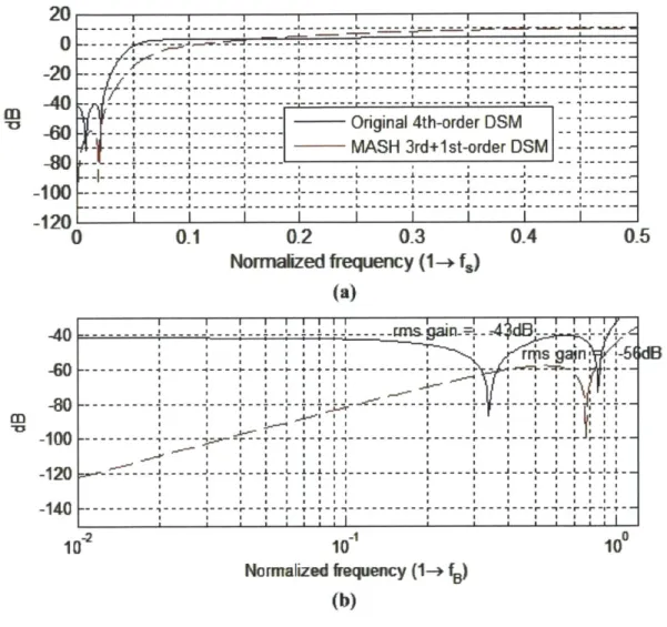
The stability advantage is directly reflected by the overall NTF of a MASH AE modulator. 20 0 -20 40 -60 -80 -100 -120 C -40 -60 -80 -100 -120 -140 0.1 0.2 0.3 Nomenzed frequency (1--+ f) 0.4 I~ ~ ~ ~~ i iI ~ I ~ I. ~~ I I, L1 -- ---- 4 -- --- -- a- 1*.- --- --- - ~ a, a- - a -a ~ a a -,... a a a a a - -\ -a a ' -. T f a a a a a " -- a - I a a a ~~~ a a -aa -~ a a a a a a-a---4--- a a a a t - -a --- a 10~ Normalized kequency (1-+ fs) (b) 0.5 dB 100
Figure 3-3: NTF graphs of an original 4th-order AE modulator and a MASH 3
rd+ls-order AE modulator: (a) overall NTF, (b) NTF within the in-band frequency
Figure 3-3(a) shows the overall NTF magnitude of the original AE modulator and the MASH AE modulator. The blue graph represents the original 4th-order AE modulator, and the red graph represents the MASH AE modulator consisting of a 3rd-order 1"t-stage and a 1st-order 2nd-stage.
As shown in Figure 3-3(b), the NTF of the MASH AE modulator can be much -m I I I I I I I I I i T --- --- -- Odgna 4-4 S -- ---4 - -- --- - - -4th-orderI--- --- 1--- ---
I--- --- I--- I---
---M
lower within the in-band frequency range. The in-band rms gain is calculated, and the NTF of the MASH AE modulator suppresses in-band noise by additional 13-dB. This is because the primary stability of the MASH AE modulator is related to the
1st-stage with a 3rd-order loop filter, which is more stable than a 4th-order loop filter. On the other hand, the stability of the original AE modulator is related to the higher-order 4th-higher-order loop filter. As a result, it is possible for a MASH AE modulator to use a more aggressive NTF.
-80 --- - -- - - - --- --- --- -80 --- --- --- -- ---- -- - - -
-20O gina 4th-or r DSM -- 0 -- -- - -- - - - n- o
-M A-140 -- DSM -st-order MASH 3rd+lst-order DSM
0 0.1 0.2 0-3 0.4 0.5 0 01 0-2 03 04 0.5
Normalized frequency (1-+. fl) Normalized frequency (1-> f,)
(a) (b)
Figure 3-4: NTF graphs of an original 4th-order AE modulator and a MASH 3
'd+1-order AE modulator: (a) NTF with a 4-bit quantizer, (b) NTF with a 4-bit quantizer and gain blocks
The NTF of the MASH AE modulator can be further improved if gain blocks are used, as shown in Figure 3-4. First, the overall NTFs are redrawn by considering a 4-bit quantizer. Since E1 is canceled and E2 is reduced with gain blocks, the overall
magnitude is further reduced. When a gain-of-4 factor is used, the overall NTF of a
MASH AE modulator is lower than the NTF of an original AE modulator, not only
within the in-band frequency range, but also at the out-of-band frequency range. In summary, a MASH AE modulator has three main advantages compared to the original AE modulator with the same effective NTF order. First, the NTF of a MASH AE modulator can suppress in-band noise more aggressively. Second, the quantization noise itself can be reduced by gain blocks. Finally, the stability issue of the 2nd-stage is truly dependent on a low-order AE modulator, which has better
stability. However, these advantages can be obtained, only if digital filters are well matched to analog filters. This matching requirement causes several practical issues that degrade the performance significantly. This problem is presented in the following section.
3.3
CT MASH
AE
Modulator
So far, only the DT MASH AE modulator has been discussed. However, as mentioned in the previous chapter, to achieve high resolution at high sampling frequencies, the
MASH architecture can be implemented in CT. However, it is not straightforward to
convert DT loop filters to CT loop filters as mentioned in the previous chapter.
Y
(a)
Output
-Quantier Output (
--Delay Block Output
(
T
(b)
Figure 3-5: Block diagram of a CT 2-stage MASH AE modulator: (a) block diagram,
(b) output of a quantizer and a delay block
modula-tor, which is comparable to the previous DT 2-stage MASH AE modulator shown in Figure 3-2. This block diagram not only highlights the difference from a DT MASH
AE modulator, but also the main issues of a CT MASH AE modulator.
First, the loop filters are replaced by CT elements, based on the impulse response matching technique, mentioned in the previous chapter. Additionally, delay blocks are required at the output of the quantizers. Since the quantizer cannot generate its output instantly as shown in Figure 3-5(b), a delay block such as a latch provides enough time for the quantization output to settle. The delay time is usually less than one sampling clock period and in this block diagram, half a clock period is used. Use of the delay block brings about two issues. First, this intentional delay, which can be considered ELD, should be compensated to make the AE modulator stable. Therefore, another feedback path, represented by a dashed line toward each loop filter, is added. The second issue is that since the manipulable output of a quantizer is obtained with a delay, the extractable quantization noise should be delayed as well. To generate a correct delayed quantization noise, the input of quantizer needs to be also delayed. For this reason, another delay block is added at the input of the quantizer. However, since the input of the quantizer is a CT signal, in order to delay this signal, a SH circuit or an analog delay line is required. The sampled signal from a SH circuit can then be delayed by a half or a full clock period. The issue here is that it is difficult to implement an accurate SH circuit for sampling frequencies over 1-GHz. Also, since the SH circuit is added directly to the output of the loop filter, the loading effects from the SH circuit could cause negative effects on the original loop filter. Analog delay line with a precise delay is also difficult to implement.
The most serious problem of CT MASH AE modulators occurs at the digital filters. In Figure 3-5(a), digital filters are designed as STF2 and NTFi, respectively.
In order to cancel Ei, digital filters should be well matched with the analog filters. If the digital filters are not well matched, the output of the CT MASH AE modulator is given by:
Y STF1,A -STF2,D .X + (NTF1,A -STF2,D - STF2,A - NTF1,D) -E1
-NTF1,D -NTF2,A - E2 (3.3)
Subscript A and D represent the analog and digital filters, respectively. As shown in Equation 3.3, to completely cancel E1, NTF1,D and STF2,D must be the same
as NTF1,A and STF2,A, respectively. Therefore, if analog and digital filters are not
well matched, the second term in this equation, cannot be fully suppressed. The uncanceled portion of Ei then leaks to the output, degrading the SNR of the CT
MASH A E modulator, since it is not suppressed by the high-order NTF, NTF1 -NTF2.
Although both analog and digital filters target matched STF and NTF to fully cancel
Ei, the analog filter transfer characteristic is modified by fabrication mismatches
and other non-idealities. These non-idealities include significant RC variation and additional errors due to finite op-amp DC gain and UGBW. Therefore, NTF1,A and
STF2,A resulting from the analog loop filters cannot be naturally matched to digital
filters without additional calibration. Also, since the CT loop filter is used in the 2nd"stage, it is difficult to implement STF2,A in the z-domain perfectly with a digital
filter. Therefore, only an approximate STF2,D can be used as the digital filter, causing
further mismatches between analog and digital filters.
3.4
Previous Work
Due to several issue with CT MASH AE modulators, there are only a few published papers with results from experimentally tested circuits [26][27][28][29]. These pre-vious works focus mainly on matching analog and digital filters, in order to fully cancel quantization noise. Several methodologies have been explored, but since loop filters and digital filters were implemented based on the specific cascaded architec-tures [25] [30], there was the limitation to choose NTF. Moreover, the effect of the delay block at the output of a quantizer was ignored. Table 3.1 summarizes the
Table 3.1: Performance table of prior CT AE modulators [26] [27] [28] [29] [31] [32] [33] Target Fs(GHz) 0.36 0.208 0.16 0.34 0.64 4 3.6 2 BW(MHz) 18 10/15 10 20 20 125 36 50 DR(dB) 68 70/61 67 77 80 70 83 84 Peak SNDR(dB) 62.5 61/55 56 69 74 65 70.9 80 Power(mW) 183 10.5 68 56 20 256 15 100
Technology 0.18umn 65nm 0.18um 90nm 130nm 45nm 90nm 28nm
FOM(pJ/step)1 4.66 0.57/0.76 6.59 0.61 0.12 0.70 0.073 0.122
FOM(pJ/step)2 2.47 0.14/0.38 1.86 0.24 0.06 0.40 0.018 0.077
FOM(dB)3 147.9 159.8/152.5 148.7 162.5 170 156.9 176.8 171
performance of four previous papers and recent state-of-the-art publications [31] [32]
[33] with target specifications of the proposed AE modulator. The proposed target
specifications are relevant for future wireless communication applications. There are
three different types of FOMs: FOM' =NDR-1.76 , FOM DR-1.76,
2.BW-2 6.2_ 2.BW.2 _6.02_
and FOM3 = DRdB + 10 log(Bw), when SNDR represents the signal-to-noise and
distortion ratio. As shown in this table, due to several limitations of the previous publications, adequate DR and FOM for the target specification were not achieved.
Therefore, to meet all design requirements, a new CT AE modulator architecture needs to be developed. In the following chapter, a new CT AE modulator is presented
Chapter 4
A New CT MASH
AE
Modulator
The ideal MASH AE modulator provides several significant advantages. Specifically, it allows for a high-order noise shaping characteristic with improved stability. In spite of its advantages, the MASH AE modulator has seen limited use, since physical
MASH AE modulator implementations often encounter many practical problems. In
particular, CT MASH AE modulators have several problems mentioned in the pre-vious chapter, such as delaying CT signal and matching filter requirements. In this chapter, a new CT MASH AE modulator, which circumvents the critical problems of conventional CT MASH AE modulators is proposed. The goal of the proposed AE modulator is to suppress quantization noise such that it does not limit the target res-olution and bandwidth, 84-dB and 50-MHz respectively, for the intended application. At the same time, this AZ modulator eases the requirements of its component match-ing. To demonstrate the concept, a CT 2-stage MASH architecture with a 4th-order overall NTF is designed for the proposed CT MASH AE modulator. In the 1"-stage, a 3rd-order loop filter is used, and a 1"s-order loop filter is used in the 2nd-stage.
4.1
DT Sturdy-MASH
AE
Modulator
The most serious problem of MASH AE modulators is the matching issue between analog and digital filters. If these two filters are not well matched, the quantization noise from the 1s"-stage cannot be completely eliminated. Since the actual analog filter
transfer function is sensitive to fabrication tolerances, special methods are needed for
MASH AE modulators to achieve matched analog and digital filters. Under such
methods, either the analog or digital filters must be calibrated. To do this, additional circuitry is needed to implement calibration algorithms, causing design complexity. To avoid this problem, a new MASH architecture, referred to as sturdy-MASH [34], was propsed. The block diagram of a sturdy-MASH AE modulator is shown in Figure 4-1.
X
Figure 4-1: Block diagram of a sturdy-MASH AE modulator
Based on Figure 4-1, the output transfer function is represented by:
Y
Y STF1-X+NTF1 -[E1 -(STF 2-E1l+NTF2 -E2)]
STF1-X + NTF1 - (1 - STF2) -E1 - NTF1 -NTF2-E2
(4.1) (4.2)
In this equation, the quantization noise from the 1"s-stage, E1 is not eliminated,
unlike Ei of a conventional MASH AE modulator. However, if the 2nd-stage is de-signed such that (1-STF2) is equal to NTF2, the output transfer function is given
Y - STF1 -X + NTF1 - NTF2 -E1 - NTF1 - NTF2 -E2 (4.3)
Thus, E1 and E2 can be simultaneously shaped by NTF1-NTF2, which is of the
same order NTF as a conventional MASH AE modulator. For example, NTF, NTF2, and STF2 in [34] are given by:
NTF 1- (I1 z-1)2 , NTF2 = (1 - z- 1)2, and STF2 = (1
-z-1 )2 (4.4)
1 - z-1 + 0.5z-2
Therefore, the overall NTF, which suppresses Ei and E2, is given by:
NTFoverau = -I 1 O-1z 2 (4.5)
1 - z- + 0.5z-2
[34] uses a 2-stage structure with a 2nd-order loop filter used in each stage. As a result, the overall NTF becomes 4th -order. Quantization errors, Ei and E2, are
suppressed by the 4th-order NTF, but stability of the entire modulator is dictated by the 2nd-order loop filter, which is inherently more stable.
Equation 4.3 shows that a sturdy-MASH AE modulator can provide the same ad-vantage that an original MASH AE modulator. Theoretically, the only disadad-vantage is that since E1 cannot be perfectly eliminated, there is a 3-dB degradation in SQNR, assuming Ei and E2 are uncorrelated. By paying this cost, quantization noises, E1 and E2, are suppressed by the high-order NTF, NTF1 -NTF2 without requiring
digi-tal filters matched to analog transfer functions. Although the AE modulator shown is implemented in DT, the advantages of a sturdy-MASH architecture can also be exploited in CT. A CT MASH AE modulator based on the DT sturdy-MASH AE modulator is thus developed further in the next section.
4.2
Main Challenges and Solutions of a CT MASH
AE Modulator
Although a DT sturdy-MASH AE modulator can suppress quantization noise with a relatively high-order NTF, because it is implemented in DT, the use of high sampling frequencies to achieve increased signal bandwidth is significantly restricted. Since the achievable signal bandwidth of a DT sturdy-MASH AE modulator is below the requirements of modern wireless applications, a CT implementation is explored. The development of a CT implementation leads to several key issues, which must be resolved.
Latch
+ CT Sign z * +Y
X -4 + &irS i 14 : ...'1111i +...
Figure 4-2: Block diagram of an early version of the new CT-MASH AE modulator
Figure 4-2 shows a block diagram of an early version of the new CT MASH AE modulator. This block diagram illustrates the main challenges in the implementation of the CT MASH AE modulator. The output transfer function of this AE modulator is given by:
Y = STF1 -X + NTF1 -(1 - STF2) - E1 - NTF1 -NTF2- E2 (4.6)