Delta-Sigma Digital-RF Modulation for High Data
Rate Transmitters
by
Albert Jerng
B.S. Electrical Engineering
Stanford University, 1994
M.S. Electrical Engineering
Stanford University, 1996
Submitted to the Department of Electrical Engineering and Computer
Science
in partial fulfillment of the requirements for the degree of
Doctor of Philosophy in Electrical Engineering and Computer Science
at the
MASSACHUSETTS INSTITUTE OF TECHNOLOGY
Sept Z006
Sept ý006
@
Massachusetts Institute of Technology 2006. All rights reserved.
Author
partment of lectrical Engineering and Computer Science
Department of Q letrical Engineering and Comput'er" S' ience
September 21, 2006
C ertified by
.... ... .
...
Charles G. Sodini
-IProfessor
Th
2iess Supervisor
MASSACHUSErr
OF TECHNAPR
3 0
Accepted by...
.-...
. ...
Arthur C. Smith
LIBRARIES
Uhairman, Department Committee on Graduate Students
ARCHIVES
S
INSTITUTEOLOGY
Delta-Sigma Digital-RF Modulation for High Data Rate
Transmitters
by
Albert Jerng
Submitted to the Department of Electrical Engineering and Computer Science on September 21, 2006, in partial fulfillment of the
requirements for the degree of
Doctor of Philosophy in Electrical Engineering and Computer Science
Abstract
A low power, wideband wireless transmitter utilizing AE direct digital modulation of an RF carrier is presented. The transmitter architecture replaces high dynamic range analog circuits with high speed digital circuits and a passive LC bandpass filter, saving power and area compared to conventional IQ modulators for wideband systems. A prototype transmitter IC built in 0.13 pm CMOS demonstrates a data rate of 1.2 Gb/s using OFDM modulation in a bandwidth of 200 MHz centered at 5.25 GHz. The modulator consumes 187 mW and occupies a die area of 0.72 mm2. A quadrature digital-IF approach eliminates modulator LO feedthrough and image spurs from the output spectrum without requiring analog circuitry or system calibration, simplifying the design of the transmitter. The largest modulator spur is measured to be -47 dBc.
Measured SNDR over a 200 MHz bandwidth is 43 dB.
Successful implementation of the AE RF modulator requires the design of a high-Q, tunable RF bandpass filter, and a low power, high speed digital AE modulator. A 4th order passive LC bandpass filter with center frequency of 5.25 GHz is designed and implemented using differential coupled resonators. Variation of the filter response over process and temperature is removed through the design of an automatic self-tuning loop that calibrates the filter center frequency to the system LO. A 2.625 GS/s, 2nd order, 3-bit digital AE modulator is realized through the use of a pass-gate adder circuit optimized for low power and high speed.
The digital modulator is software programmable to support multiple bandwidths, frequency channels, and modulation schemes. It can be used adaptively to transmit in selected channels with variable bit-rates, depending on channel conditions. It is envisioned that the AE digital-RF modulator can be used as a universal transmitter for wideband systems and applications that require high data rates and low power consumption.
Thesis Supervisor: Charles G. Sodini Title: Professor
Acknowledgments
The completion of my PhD program has been a very rewarding process and
experi-ence. In particular, I have been enriched by the interactions with faculty, and fellow
students both inside and outside the classroom and lab. I'd like to thank my advisor
Prof. Charles Sodini
-
his guidance and judgement throughout my thesis project has
been greatly appreciated. Thanks for pushing me with thought-provoking questions,
which helped me realize the full potential of this project. I'd like to thank my
com-mittee member Prof. Anantha Chandrakasan for providing me with knowledge on
digital design issues and giving me a kickstart on the high speed adder design. I'd like
to thank my committee member Prof. Mike Perrott for providing helpful suggestions
on the phase detector design in my tuning loop, providing advice throughout my
pro-gram, and sharing lab equipment with our group. I'd also like to thank Prof. Vladimir
Stoyanovic for helpful discussions regarding high speed digital interfaces. During my
summer at ADI, I got some great feedback regarding my project. In particular, I'd
like to thank Bill Schofield and Richard Schreier for their helpful discussions and
comnments.
I have enjoyed the comaraderie and help of many labmates over the years. Andy
Wang was a great source of knowledge on system issues. Todd Sepke has helped me
a lot through technical discussions, and by proofreading papers for me. Anh Pham
provided great advice on RF board design and was a magician soldering ICs for me.
Lunal Khuon provided lots of helpful lab parts and was a great conference roommate
and fellow senior citizen/dad. Andrew Chen was a great die photographer and helped
me out on digital testability issues. Ken Tan, Nir Matalon, Farinaz Edalat, and Khoa
Nguyen helped me understand the WiGLAN system and use the boards to test EVM
on my transmitter. Mark Spaeth provided lots of help with PCB design questions and
lab troubles. It has been fun socializing with the all the above and other members of
the lab John Fiorenza, Matt Guyton, Albert Chow, Johnna Powell, and Kevin Ryu.
I'd also like to thank Rhonda Maynard for all her help with taking care of purchase
orders, and quotes, and reimbursements, and just making life easier for me.
I'd like to thank my family and friends for always being there for me. To my parents, thank you for all your support over the years, and for providing the framework that makes this all possible. To my wife, Veronica, thank you for embracing the change of lifestyle and weather so whole-heartedly, and for being such a good mother and partner. And to my little one, Elliot, thank you for brightening each day with your smile.
Contents
1 Introduction
1.1 WiGLAN Transmitter
...
1.2 Conventional IQ Transmitter .
...
1.2.1
IQ Modulator Impairments .
...
1.3
AZ Digital-RF Modulation
...
1.3.1
Process Scaling .
...
1.3.2
Circuit Integration .
...
2 Digital-RF Conversion
2.1 Previous Research ...
2.2 RF Bandpass Reconstruction Filter .
...
2.3 Filtering Requirements .
...
3 LC Bandpass Filter Design
3.1 Challenges . ...
3.2 Differential Coupled Resonator Topology
3.2.1
Area Considerations ...
3.2.2
Impedance Considerations .
3.2.3
Inductor Design ...
3.2.4
Varactor Design ...
3.2.5
5.25 GHz Filter Design ...
3.3 Automatic Tuning Loop ...
3.3.1
Non-Idealities ...
7
3.4 3.5 3.6 4 AE 4.1 4.2 4.3 4.4 4.5
3.3.2 Digital Tuning Loop... Q-enhancement . ... Test Filter Measurements ... Summary ...
System Architecture
Choosing Clock Frequency ... Co-Design of AE NTF and RF BPF Comparison to Oversampling with No UWB System Example ...
Summary ...
Noise-Shaping
5 Quadrature Digital-IF AE Modulator
5.1 Digital-IF ...
5.2 Quadrature Digital-IF ... 5.2.1 Bandpass AE ... 5.3 Frequency Planning ... 5.4 Summary ...
6 Digital Circuit Design
6.1 Low Power Design Challenges ... 6.1.1 General Techniques ... 6.2 AE Modulator Topology . ...
6.3 Low Power, High Speed Adder Design .
6.3.1 Conventional Static Mirror Adder 6.3.2 Passgate Adder . ...
6.4 Top Level Implementation and Results . 6.4.1 Interpolation Filter . ... 6.4.2 Digital-IF Up-Converter ... 6.4.3 Simulation . ... 6.5 Summary . .... ... 93 93 94 96 99 99 102 107 108 110 110 112
7 DRFC Circuit Design
113
7.1
Unit Cell Mismatches ...
114
7.1.1
DAC Mismatches ...
...
115
7.1.2
AE DRFC Mismatches ...
...
118
7.2 Behavioral Simulations ...
120
7.2.1
LO Phase Mismatch ...
...
...
124
7.3 Circuit Implications ...
...
124
7.4 DRFC Unit Cell Implementation ...
.
126
7.5 Simulation Results ...
...
130
7.6 Summary
...
...
134
8 Measurement Results
135
8.1 Fabricated Test Chips ...
...
...
135
8.2 Test Setup
...
.
...
138
8.3 Test Chip Results ...
...
139
8.4 Power/Area Comparison ...
...
150
9 Conclusion
153
9.1
Future Directions ...
.
..
...
154
List of Figures
1-1
Conventional IQ Modulator ...
....
22
1-2 IQ Modulator Output Spectrum ...
..
25
1-3 Digital QPSK Modulator ...
...
26
1-4 Digital AE RF Modulator ...
...
27
2-1 RF DAC Unit Cell ...
..
...
30
2-2 DRFC Unit Cell ...
.
...
31
2-3 Up-Converted Clock Images ...
....
32
2-4 Up-Converted Quantization Noise ...
.
32
2-5 Quadrature Digital-RF Converter Core . ...
33
3-1
Filter Topology ...
...
.
...
38
3-2 Differential Resonator with Non-linear C(V) . ...
.
43
3-3 LC BPF Schematic ...
...
.
45
3-4 Differential Inductor Lumped Element Model . ...
45
3-5 Differential Tank Capacitance C(V) . ...
46
3-6 Coupled Resonator Model ...
...
48
3-7 Tuning Loop Block Diagram ...
....
49
3-8 Tuning Loop Model ...
...
...
50
3-9 Filter Block and Phase Detector Transfer Functions ...
.
51
3-10 Phase Detector Schematic ...
...
.
....
. .
52
3-11 Filter Block Transfer Function vs. Temperature . ...
53
3-12 Phase Detector Transfer Function . ...
.
54
3-14 Filter Response ... .. ... 56
3-15 Q-enhanced Resonator Model ... ... 57
3-16 Simplified Test Filter Schematic ... .. 61
3-17 Test Filter Die Photo ... ... 62
3-18 Filter Response vs. Vtune ... ... 63
3-19 Automatic vs. Manual Tuning ... ... 63
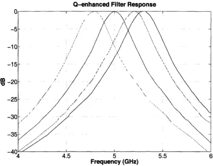
3-20 Q-enhanced Filter Response Tuning Curves . ... 64
3-21 Automatic vs. Manual Tuning, Q-enhanced version . ... 65
3-22 Measured Filter with and without Q-enhancement . ... 65
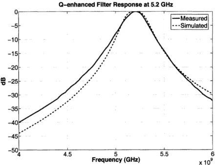
3-23 Q-enhanced Filter : Measured vs. Simulated . ... 66
4-1 AE Digital-RF Modulator ... ... 67
4-2 AE Modulator Output Spectrum ... . 68
4-3 Aliasing Problem in Up-Conversion . ... 69
4-4 No Aliasing with fLo = 2
flk
... ... 704-5 Normalized Magnitude of Zero-Order Hold Frequency Response . . . 71
4-6 Image Rejection vs. OSR ... ... 71
4-7 SNR (dB) vs. Loop Filter Order for various OSR . ... 73
4-8 RF Output Spectrum using 3rd order, 1-bit AE Modulator ... 74
4-9 RF Output Spectrum using 2nd order, 3-bit AE Modulator ... 75
4-10 UWB Output Spectrum using System Parameters from Table 4.3 . . 78
5-1 Digital-IF AE RF Modulator . ... .. 82
5-2 Aliasing when fIF = LK ... . . . . . . . ... 84
5-3 Quadrature Digital-IF AE RF Modulator . ... . 84
5-4 SNR vs. LO Phase Error for Quadrature Digital-IF . ... 85
5-5 Digital-IF Bandpass AE Modulator . ... 86
5-6 Single PLL LO Generation for Digital-IF Architecture ... . 88
5-7 Zero Order Hold Impulse Response . ... 89
5-8 Frequency Response of Zero Order Hold . ... 90
6-1 Pipeline of (4) 3-bit Ripple Carry Adders ...
6-2 Pipeline of (2) 6-bit Ripple Carry Adders ...
6-3 Error Feedback Topology . ...
6-4 2nd Order MASH Error Feedback Topology . . . .
6-5 MATLAB Simulation of 2nd Order, 3-bit AE Modulator
6-6 Mirror Adder Even Cell .
...
6-7 Mirror Adder Odd Cell ...
6-8 NMOS Passgate Adder Simplified Schematic ...
6-9 PMOS Sense Amplifier ...
6-10 RC Network to Model Carry Chain Delay . . . ..
6-11 Passgate Adder Transistor-Level Schematic ...
6-12 Pass-Gate Adder Carry Chain Waveforms . . . ..
6-13 Digital Block Diagram ...
6-14 4x Interpolator Implementation . ...
6-15 Digital-IF I,Q Bitstreams. ...
6-16 Digital-IF Up-Converter Implementation ...
6-17 Verification of Digital Block ...
7-1
7-2
7-3
7-4
7-5
7-6
7-7
7-8
7-9
7-10
7-11
Quadrature Digital-RF Converter Core .
DRFC Unit Cell Mismatches . . . .
LO Amplitude Mismatch . . . ..
LO Phase Mismatch ...
Data Timing Error ...
Behavioral Mismatch Simulation . . . . .
SNDR (Mean) vs. Percent Mismatch . .
SNDR (Std Dev) vs. Percent Mismatch.
LO Timing Spread vs. Gain Mismatch
SNDR vs. LO Delay/Segment . . . .
Unit Cell Transistor Mismatches . . . . .
. . . .
.
94
. . . .
.
95
. . . .
.
96
. . . .
.
97
. . . .
.
98
. . . . .
100
. . . . .
100
. . . . .
102
. . . .
.
103
. . . .
.
104
. . . .
.
105
. . . .
.
106
. . . .
.
107
. . . .
.
108
. . . .
.
109
. . . .
.
109
... 111. . . . .
. . . .
.
114
.
. . . . .
.
116
.
. . . . .
.
117
.
. . . .
.
118
.
. . . .
.
119
.
.
. . . .
.
121
. . . .
. . . . .
.
122
. . . . .
. . . . .
.
122
. . . .
. . . . .
.
123
.
.
. . . . .
.
123
. . .
. . . . .
.
125
7-12 LO Differential Pair Output Current Matching .
1267-13
7-14
7-15
7-16
7-17
7-18
7-19
7-20
7-21
7-22
Test Chip 1 Block Diagram
Test Chip 2 Block Diagram .
Testing Setup ...
8-4 Test Chip 1 :
Test Chip 1 :
Test Chip 1 :
Test Chip 1 :
Test Chip 2 :
Test Chip 2 :
Test Chip 2 :
Test Chip 2 :
Test Chip 2 :
Test Chip 2 :
Test Chip 2 :
Test Chip 2 :
12 MHz Input ...
102 MHz Input ...
Wideband Plot ...
OFDM Signal ...
..
Direct Up-Conversion of 12 MHz Input . .
Two-Tone Simulation
. . . .
Digital-IF, 12 MHz ...
Digital-IF, 12 MHz, Shift Clock Frequency
Digital-IF, Wideband Plot ...
200 MHz OFDM Signal ...
20 MHz OFDM Channel for 802.11a. ....
Pair of 20 MHz OFDM Channels . . . . .
8-16 SNR Measurement using WiGLAN Receiver
.
. . .
8-17 Test Chip 1 Die Photo . ...
8-18 Test Chip 2 Die Photo ...
. . . . .
.
136
. . . . .
.
137
. . . .
.
138
. . . . .
.
139
. . . . .
.
140
. . . . .
.
141
. . . . .
.
141
. . . .
.
142
. . . . .
.
143
. . . . .
.
144
. . . .
144
. . . . .
.
145
. . . . .
.
146
. . . .
.
146
. . . .
147
. . . .
147
. . . .
.
149
. . . . .
.
149
DRFC Unit Cell and Data Driver .
. . . .
. . . .
.
Differential Output Current of Unit Cell . . . .
. . . ..
Combined Sum of Unit Cell Currents .
. . . . .
. . . .
...
Quadrature DRFC Filtered Output .
. . . .
. . . ..
FFT of QDRFC Output .
...
. . . .
.
. . . ..
FFT of Digital-IF QDRFC Output .
. . . .
. . . .
.
Simulation of Extracted Layout .
. . . .
. . . ..
Simulation of Revised Extracted Layout . . . . .
. . . .
...
Simulation of Quadrature Digital-IF DRFC using Extracted Layout
Simulation of Quadrature Digital-IF DRFC using Revised Extracted
Layout
...
...
127
128
129
129
130
131
132
133
133
134
8-1
8-2
8-3
8-5
8-6
8-7
8-8
8-9
8-10
8-11
8-12
8-13
8-14
8-15
9-1 Element Rotation Hardware Implementation . . . .. . . . . ... .. . 155 9-2 Behavioral Model Simulation using Element Rotation .... ... . 155
List of Tables
1.1
Target SNR for WiGLAN Transmitter...
3.1 2nd Order Bessel k and q values
.
. . . . .
. . . .
3.2 Simulated Inductor
Q
at 2 GHz ...
. . . . .
. . . .
.
3.3 Filter Performance with Resonator Mismatch . . . ..
3.4 Current vs. Q-enhancement for DR=60 dB over 200 MHz BW
.
. . .
4.1 Simulated AE SNR with OSR=13 ...
4.2 Clock Image Attenuation vs. Clock Frequency for 200 MHz RF BW .
4.3 UWB System Example (Band 1, Channel 2 at 3.96 GHz) ...
39
41
55
60
5.1 LO, Clock, and IF frequencies for DIVIDE
=
8 or 16 ...
.
91
6.1 Pipelined 2-bit Mirror Adder Simulation Results ...
. . .
101
6.2 6-bit Pass-Gate Adder Simulation Results . ...
106
6.3 Digital Block Simulation Summary . ...
112
8.1
AE Modulator Power Consumption/Die Area . ...
148
8.2 FOM Comparison ...
...
150
8.3 Conventional IQ Modulator Implementation . ...
151
Chapter 1
Introduction
This research introduces a new transmitter architecture that targets high data rate wideband systems. AE digital-RF modulation efficiently modulates an RF carrier with very wide bandwidths. A wideband digital-RF modulator can be software-defined to transmit multiple frequency channels, with variable bandwidths and mod-ulation schemes, within the band. Thus, the modulator can be programmed to utilize a band of spectrum on an adaptive basis, depending on wireless channel conditions and interferers, or upon the specifications of a given standard.
Next generation wireless systems such as 802.11n and UWB aim to provide higher data rates approaching 1 Gb/s in order to support demand for high data rate wireless communications. These systems use OFDM modulation in order to utilize spectrum efficiently, leading to high peak to average power ratios and high dynamic range requirements. As data rates and signal bandwidths increase, the DAC, analog recon-struction filter, and analog mixer found in conventional IQ transmitters become more difficult to design given constraints on power, noise, and linearity. The scaling of CMOS transistors and supply voltages creates further challenges from the standpoint of dynamic range. A transmitter architecture based on AE direct digital modulation of the RF carrier replaces high dynamic range analog circuits with high speed digital circuits, and enables power and area savings in the implementation of a wideband transmitter as CMOS transistors continue scaling. This thesis makes the following contributions.
1. Design of a wideband direct digital-RF modulator architecture that efficiently provides Gb/s data rates.
2. Integration of a digital-RF converter with an RF bandpass reconstruction filter, eliminating spurious signals and noise associated with digital-RF conversion. 3. Demonstration of a quadrature digital-IF AE RF Modulator with < -60 dBc
LO and image spurious signals.
Successful implementation of the AE Digital-RF modulator was enabled through the design of two novel circuit blocks.
1. A high-Q passive LC bandpass filter with automatic center frequency tuning loop.
2. A low power 2.6 GS/s Digital AE modulator utilizing an adder design based on NMOS passgate chains and sense-amplifier flip-flops.
The outline of the thesis will be as follows. A Wireless Gigabit Local Area Network (WiGLAN) project that aims to provide Gb/s data rates for next generation networks will be introduced. Conventional IQ transmitter design will be discussed and the new
AE Digital-RF modulator will be introduced. Design details of the high-Q tunable
LC bandpass filter and AE system architecture will be presented, and the importance of co-designing the digital AE modulator and RF BPF will be explained. The method and benefits of quadrature digital-IF up-conversion will be described. The design of the high speed digital modulator and current-switching digital-RF converter will be presented. Finally, measurement results from two test-chips will be provided and the thesis will conclude with a power and area comparison between the new architecture and the conventional IQ modulator.
1.1
WiGLAN Transmitter
The WiGLAN transmitter aims to achieve Gb/s data rates by increasing the RF bandwidth to 200 MHz, employing an adaptive M-ary QAM modulation format up to
Table 1.1: Target SNR for WiGLAN Transmitter
256-QAM SNR 30 dB
Peak-Average Symbol Power 4 dB
Peak-Average Power Ratio due to multiple sub-carriers 15 dB
TOTAL 49 dB
256-QAM, and utilizing spatial diversity gain from a multiple-input multiple-output (MIMO) antenna system and MIMO signal processing. WiGLAN uses an OFDM frequency multiplexing scheme with a 1 MHz sub-carrier spacing to increase spectral efficiency and mitigate the effects of multipath. It intends to operate in the 5.15-5.35 GHz UN-II band with a center frequency of 5.25 GHz. If 256-QAM is used on all 200 sub-carriers, a raw throughput of 1.6 Gb/s can be achieved.
While the large number of constellation points in 256-QAM increases the data. rate for a given symbol rate, it also raises the required SNR of the transmit signal. Because the constellation points are closer together for a fixed transmit power, it takes smaller amounts of random noise to cause symbol decision errors. Also, because information is encoded in the amplitude of the symbol as well as its phase, a transmitter with high linearity is required to avoid compression of the signal. Further exacerbating the situation is the fact that in OFDM systems, the peak-to-average power ratio (PAPR) is high because the transmit signal is the aggregate sum of a large number of sub-carriers. Coherent addition of the sub-carriers in phase results in large signal peaks. As a result of these system choices, the transmit signal dynamic range requirements increase significantly.
Assuming an SNR requirement of 30 dB [1] due to additive white gaussian noise (AWGN) for 256-QAM, the proposed WiGLAN system would require - 50 dB of dynamic range according to Table 1.1. In addition to AWGN, other impairments that can affect the BER performance include phase noise, narrowband interference, and group delay variation. It has been shown that while phase noise and group delay variation specifications require approximately 6 dB higher performance in 256-QAM
10
Modulator
- - - - -- -- - - - - - - - ---. .
a
Figure 1-1: Conventional IQ Modulator
compared to 64-QAM, signal to interferer (S/I) ratios must increase by approxi-mately 12 dB when going from 64-QAM to 256-QAM [1]. LO feedthrough and image rejection performance determine the level of narrowband interferers generated in IQ transmitters. A S/I ratio of roughly 37 dB is required for 256-QAM [1].
The challenge for the WiGLAN transmitter is achieving high dynamic range over a wide RF bandwidth with excellent LO and image spurious performance. Currently, the widest RF bandwidth supported by 802.11 systems is 20 MHz [2].
1.2
Conventional IQ Transmitter
Fig. 1-1 shows a block diagram of a conventional IQ transmitter used to up-convert digital baseband signals to an intermediate or final RF frequency. The output of the IQ modulator can be mathematically written as
I cos(w t) +
Q
sin(w t) = A cos(w t + ¢) (1.1) where A= I2 + Q2 (1.2) and I S= arctan( ) (1.3)Q
This architecture is popular because it can produce arbitrary phase and/or
ampli-tude modulation. Furthermore, it is attractive in integrated implementations because
when the I and Q paths are well-matched, accurate modulation is achieved regardless
of temperature, supply, or process variations.
In order for the IQ modulator to correctly reproduce equation (1.1), the I and
Q
signal paths from the DAC to the output of the mixer must be linear and
well-matched. The analog circuits in this path must maintain noise and distortion to
levels satisfying the required dynamic range of the system. As the baseband signal
bandwidth increases, the DAC and analog filter blocks become more difficult to design.
Current-steering DAC architectures have achieved the best performance at high
sampling rates [3],[4],[5]. At high frequencies, their spurious-free dynamic range is
limited by dynamic errors rather than static DC errors. Imperfect synchronization
between the control signals of current switches causes code-dependent timing errors
[3]. The code dependency results in distortion at high frequencies. A voltage glitch
can appear at the source node of the current steering switches [4]. Any non-linear
capacitance on this source node will produce distortion [5].
Transient waveforms
that do not, settle within a clock period can alter the value of the next data sample.
This inter-symbol interference causes disturbances to circuit nodes that are
data-dependent, again introducing distortion [4].
Recent DACs with SFDR
>
60 dB
have been reported in the literature with sampling speeds greater than 1 GS/s and
output frequencies greater than several hundred MHz [4],[3]. However, reported power
consumption for these DACs are in the range of 110 mW
-
400 mW.
Power consumption in the analog reconstruction filter increases proportional to
signal bandwidth for a constant dynamic range [6]. This can be shown by writing the
following expressions for a-
filter.
NSD
v
n24kT
SD = oc -- (1.4)
Af
gm
Bandwidth oc 9 (1.5)
4kT
NoisePower
=
(NSD)(Bandwidth) c C4
(1.6)
Linearity oc (Vg, - Vt) = (1.7)
gm
Eqn. (1.7) is derived from the classical long-channel approximation for a MOS device, assuming square law behavior.
If the bandwidth of the filter is increased by a factor s while keeping noise power fixed, it follows from eqns. (1.5) and (1.6) that gm must also increase by a factor
s. If gm increases by a factor s, then to maintain the same linearity, Id must also
increase by the same factor s using eqn. (1.7). Eqn. (1.6) also indicates that analog filter design involves a fundamental tradeoff between noise and capacitor area.
1.2.1
IQ Modulator Impairments
The output spectrum of an ideal IQ modulator contains a single tone at frequency
WLO + WBB (assuming a sine-wave baseband input). In practice, spurious signals due to LO leakage, baseband harmonic distortion, and finite image rejection accompany the desired signal as shown in Fig. 1-2.
LO leakage is typically caused by random device mismatches in the baseband transconductor of the mixer. This creates a dc offset that up-converts to the LO frequency at the output of the mixer. The magnitude of the LO leakage relative to the desired output signal is proportional to the ratio between the DC offset and the baseband input signal. One can minimize LO leakage by increasing the ampli-tude of the baseband signal. The tradeoff is that the baseband harmonic distortion increases when the signal amplitude is increased. The transconductor is typically designed to keep harmonic distortion < -50 dBc at the expense of LO leakage and noise performance.
Image rejection is limited by the amplitude and phase matching of the quadra-ture LO signals and the I and Q baseband paths. Without additional calibration
10 Modulator Typical
Output Spectrum
Desired
Figure 1-2: IQ Modulator Output Spectrum
algorithms and correction circuitry, the LO and image signals are typically -30 to -40 dBc.
1.3
AE Digital-RF Modulation
This research proposes direct digital modulation of the RF carrier as the basis for a transmitter architecture that can eliminate high performance DACs and analog filters. Before discussing this architecture, we will briefly review other transmitter approaches found in the literature.
Closed loop PLL modulation directly modulates the VCO without requiring a DAC or analog filter [7]. However, the data bandwidth is limited by the relatively narrow PLL loop bandwidth required to suppress synthesizer phase noise. It is un-suitable for wideband applications with bandwidths on the order of 100 MHz.
A simple realization of wideband direct digital modulation is shown in Fig. 1-3 [8], which implements a QPSK modulator capable of generating one of four quadrature phases of the RF input. This brute-force approach is limited in its applicability. An OFDM system with multiple sub-carriers each being modulated by 256-QAM
(0LO
Digital Inputs
Figure 1-3: Digital QPSK Modulatorwould require the generation of much more than four phase angles. In addition, this approach introduces abrupt phase transitions in the RF signal. By sending the data with ideal rectangular pulses, the frequency spectrum of the output signal takes on a Sin profile, producing a wide transmitted spectrum. In order to accomodate many users and avoid interference problems, Nyquist filtering is applied to digital data in wireless transmitters to narrow the transmit spectrum without introducing inter-symbol interference (ISI). In the time domain, the data transitions are smoothed while the data points at ideal sampling instants remain unaffected.
The desire for a band-limited transmit spectrum requires the phase shifter design to have continuously adjustable phase rather than discrete phase levels. An analog phase shifter is more complicated to design and requires a DAC and analog filter to interface to digital data. In addition, accurate modulation is difficult to achieve due to changes in an analog phase shifter's characteristics over process, temperature, and voltage.
Over-sampling AE concepts [9] can be applied to create a digitally controlled vector modulator that provides a continuous range of output phase and amplitude values. In Fig. 1-4, filtered I,Q digital data are over-sampled and converted into 1-bit
0 or 180
I*cos( co t)+
Q*sin(o
t)
0
Figure 1-4: Digital AE RF Modulator
output streams by digital AE modulators. The phase shifter needs to either pass the LO signal or invert it, and can be realized trivially by a differential current steering switch in CMOS. While the quadrature LO signals being modulated toggle between only two phases, their sum represents a continuous range of phase/amplitude modu-lation based on the duty cycle of the over-sampled AE bit-stream. The modumodu-lation of the RF carrier is correctly encoded but obscured by a large amount of high frequency quantization noise. An RF bandpass filter removes the out-band quantization noise and reconstructs the modulated RF signal. The concept can be extended to multi-bit
AE modulators using binary weighted or unary weighted LO current steering cells.
This architecture replaces the DAC, analog reconstruction filter, and analog mixer with a high speed AE modulator, a digital-RF converter (DRFC) based on current steering switches, and a passive RF BPF. The primary advantage is that the analog baseband signal path has been eliminated, removing noise and linearity considerations from the design and enabling power and area savings for wide bandwidths. Both baseband and RF inputs to the DRFC are fully switching digital signals and no distortion results from signal clipping. In addition, a passive RF BPF consumes no power and has little noise and distortion, in contrast to active analog filtering.
1.3.1
Process Scaling
The analog circuit design in conventional IQ transmitters becomes even more chal-lenging as transistor sizes and supply voltages continue scaling downward. However,
the AE digital-RF modulator benefits from the faster digital circuits available from
scaled CMOS processes. Scaling directly reduces the power and area of the high
speed digital AE modulator. In digital process scaling, there has also been a trend of
increasing levels of metallization and lower resistance routing. As a result, on-chip
in-ductors with higher Q can be built using lower loss metals that are farther away from
the substrate. Higher inductor Q allows the design of sharper, more selective passive
bandpass filters, improving the quantization noise suppression of a AE digital-RF
modulator.
1.3.2
Circuit Integration
In conventional IQ transmitters, the DAC, analog reconstruction filter, and analog
mixer are designed as distinct blocks that must interface to each other. The DAC is
often on a separate digital chip. Each block contributes its own noise and distortion
to the transmit signal. In order to meet the dynamic range specifications of the
transmitter, each individual block must be designed such that its dynamic range
exceeds the overall specifications. The AE digital-RF modulator can be integrated in
a digital CMOS process. In addition, the DRFC and bandpass filter can be combined
into a single circuit structure, as will be shown in the next chapter. Noise and linearity
constraints do not apply to the digital circuits, and only mismatches between DRFC
current-steering switch cells can cause distortion, as will be discussed later.
Chapter 2
Digital-RF Conversion
In a conventional transmitter, the digital baseband signal is first converted to an analog signal using a DAC, and then up-converted to RF frequency using a mixer. A digital-RF converter (DRFC) combines these two steps into one circuit. The DRFC inputs are the digital baseband bits and the DRFC output contains the analog base-band signal modulated around an RF carrier.
2.1
Previous Research
A radio frequency digital-analog converter (RF DAC) was introduced in [10]. In general, the output of a DAC contains the desired analog signal as well as its images around each multiple of the DAC clock frequency. The RF DAC uses one of these high frequency clock images as an RF output. A simple schematic representation of an RF DAC unit cell is shown in Fig. 2-1. A sine-wave at the desired clock image frequency modulates the DC bias voltage of the DAC current source. This increases the clock image power by mixing the DAC impulse response to the clock image frequency. One drawback is that the RF DAC outputs substantial energy at other frequencies, including its primary output near DC.
The digital-RF converter (DRFC) in [11] features a balanced version of the RF DAC unit cell, as shown in Fig. 2-2. The balanced unit cell is a more efficient RF modulator because the low frequency response around DC is rejected and the RF
RF
DAC Unit Cell
Digit
Data
Vbias
Figure 2-1: RF DAC Unit Cell
output is now the primary output. This balanced unit cell is identical in structure to a Gilbert-cell mixer. The difference is that in a DRFC, the digital baseband inputs directly drive the top pair of current-steering switches, multiplying an RF carrier signal by
+1
based on the digital data. In contrast, the Gilbert-cell mixer's bottom differential pair is driven by an analog baseband signal and must be linearized.The DRFC performs a mixing operation between the digital baseband signal and the local oscillator signal to produce a modulated RF output. It merges the func-tions of the DAC and mixer, while eliminating the analog filtering between the two. However, the frequency spectrum of the digital signal repeats itself at all multiples of the sampling rate or clock frequency. These clock images are up-converted by the DRFC without any filtering besides the sinc response associated with the zero-order hold in the digital-RF interface. When using a digital AE modulator, high frequency shaped quantization noise is up-converted without any filtering. In either case, an RF bandpass filter is required at the output of the DRFC, as illustrated in Fig. 2-3 and Fig. 2-4. In the previous work [10], [11], substantial off-chip filtering is required to eliminate high frequency clock images and quantization noise and produce a clean
Digital-RF Converter Unit Cell
Digital
Data
+
Figure 2-2: DRFC Unit Cell
transmit spectrum. The fundamental difficulty with direct digital-RF conversion is the transmission of spurious emissions outside the signal band that are difficult to filter at RF frequencies.
One approach to the filtering problem involves embedding a semi-digital FIR reconstruction filter in the digital-RF interface. In [12], the 1-bit output of a AE modulator goes through a 6-tap digital delay line. Each output of the delay line is
applied to the switch input of an RF DAC cell whose current source is weighted with the appropriate FIR filter coefficient. The drawback to this approach is that a large number of taps is needed to implement an FIR filter with reasonable attenuation. For example, in [13], a 128-tap delay line realizes the equivalent transfer function of a 2nd order analog filter with -20 dB/decade slope in the stopband. For high RF output frequencies and wide baseband bandwidths with high sampling rates, a large number of delay taps and weighted current sources in the digital-RF interface will consume a large amount of power. In [12] with a 6 tap FIR filter, the RF output spectrum at 1
Up-Converted Clock Images
fLQ/fCLK fLO fLO +
Figure 2-3: Up-Converted Clock Images
Up-Converted Quantization Noise
I+
Q it
I sint wt
Figure 2-5: Quadrature Digital-RF Converter Core
GHz contains a significant amount of out-of-band quantization noise. The magnitude of this noise is approximately -35 dBc at a frequency offset of 15 MHz from a 1 GHz single-tone output.
2.2
RF Bandpass Reconstruction Filter
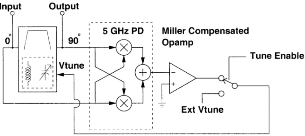
Our design integrates a high-Q passive LC bandpass filter into the load of the digital-RF conversion circuit. Fig. 2-5 shows a circuit schematic of our quadrature Ddigital-RFC with load filter.
This realization integrates both the DRFC and RF BPF under a single supply. In the unit cells, quadrature phases of an RF carrier are applied to differential pairs biased by tail current sources. The output currents of the differential pairs are routed through differential current steering switches controlled by the I and Q digital AE modulator output bits. The resulting output currents from each unit cell are summed and then filtered by a passive LC network that also performs I-V conversion. The filter does not consume any additional voltage headroom due to the inductor, and
acts as a tuned load to provide high gain for the DRFC.
Passive LC filtering at RF is attractive because it provides high dynamic range with no power consumption. At multi-GHz RF frequencies, LC filters are relatively small in terms of die area. However, the steepness of a passive LC filter's roll-off is limited by the finite
Q
of on-chip passives. The feasibility of this approach depends on the RF filtering requirements.2.3
Filtering Requirements
The required
Q
of the bandpass filter can be approximated using the relationQ
=fo
(2.1)BW
where fo is the filter center frequency and BW is the signal bandwidth. A typical narrowband wireless system such as GSM has a signal bandwidth of 200 kHz and a center frequency of 1-2 GHz, requiring a Q of 5,000-10,000. Fortunately, the required Q decreases as the signal bandwidth increases. For wideband systems with signal bandwidths on the order of 100 MHz, conventional analog filtering becomes more difficult while RF bandpass filtering becomes practical. The WiGLAN transmitter, with a bandwidth of 200 MHz and a center frequency of 5.25 GHz, requires a Q of -25, which is still difficult but possible.
The selectivity requirements of the BPF also depend on the location and mag-nitude of the spurious signals. Oversampling of the digital input signal places clock images farther out in frequency and reduces RF filtering requirements. A high speed current-steering DRFC requires accurate distribution and matching of the LO path signal [11]. For multi-GHz LO and clock frequencies and a typical segmented archi-tecture with a large number of unit cells, the power consumption of the LO and data buffers becomes substantial. Oversampling AE modulation pushes the clock images farther away and also reduces the number of unit cells required by the converter. This reduces the power consumption and area of the DRFC, and minimizes routing parasitics in a high frequency converter. The spurious signals are dominated by the
shaped out-of-band quantization noise, whose magnitude can be engineered through design of the AE noise transfer function (NTF).
In the following sections, the design of a fully integrated high-Q LC BPF and the architecture of the AE digital-RF modulator will be described. The design of the
AE modulator will be dictated by the required in-band SNR, as well as the required
Chapter 3
LC Bandpass Filter Design
3.1
Challenges
The design of a passive LC bandpass filter involves several challenges. In order to attain a sharp roll-off, the on-chip passives used in the filter must have high Q.
The finite Q of on-chip inductors typically limits the overall Q to the range of 10-20, depending on the parameters of the process. With high Q and a narrow passband, any varia.tions in capacitance or inductance over process and temperature will cause a, shift in the filter center frequency and a large amplitude loss in the fixed RF bandwidth of the system. Meanwhile, noise and spurious signals at out-of-band frequencies may fall in the shifted passband of the filter. A practical realization must include an automatic control loop to stabilize the filter center frequency over process and temperature variations. In order to attain higher resonator Q, active Q-enhancement can be added but will be accompanied by a penalty in power consumption and dynamic range.
3.2
Differential Coupled Resonator Topology
A conventional bandpass design method is to take a lowpass prototype ladder filter and perform a lowpass to bandpass transformation by placing a capacitor in series with all inductors and an inductor in parallel with all capacitors. The resulting ladder contains too many inductors, occupying large die area. A narrowband approximation
Bandpass
LC Ladder
Filter
Coupled
Resonator
Filter
Differential
Coupled
Resonators
Figure 3-1: Filter Topology
to the bandpass ladder filter can be realized with shunt LC resonator sections that are capacitively coupled [14]. This topology minimizes the number of inductors required in the filter. Further area reduction is achieved by converting the topology into its differential form, as shown in Fig. 3-1. Symmetric differentially-wound inductors take up less area than two equivalent single-ended inductors. In addition, wasteful spacing between inductors is eliminated, allowing a more compact layout. The capacitor area is reduced by a factor of 4 in the differential resonator implementation.
The coupled resonator design methodology follows in a manner analogous to con-ventional ladder design using filter look-up tables [14]. Based on the normalized resonator quality factor defined as,
11
Table 3.1: 2nd Order Bessel k and q values qo Insertion Loss (dB) q1 qn k12 00 0 0.5755 2.1478 0.8995 9.078 1.335 0.61 1.7737 0.8329 4.539 2.734 0.6523 1.4920 0.7685 3.026 4.187 0.7093 1.2606 0.7068 2.269 5.680 0.8138 1.0263 0.6486 1.816 7.270 0.9078 0.9078 0.6360 1.513 9.208 0.9078 0.9078 0.6360 1.297 11.707 0.9078 0.9078 0.6360
Af
q0 =fm
Qo (3.1)normalized coefficients of coupling k, and normalized source and load q values are tabulated for coupled ladder lowpass prototypes. In eqn. (3.1), Af is the filter bandwidth, f, is the filter center frequency, and Q0 is the unloaded resonator Q. For
example, in Table 3.1 [14], the normalized k and q values are listed for a 2nd order Bessel lowpass filter prototype.
The un-normalized bandpass parameters are given by [14]
Af
Ki,k
= k,kA
(3.2)
f
mQi = q, (3.3)
Af
Choosing an inductance value L, the filter component values can be calculated using [14]
1
= fm (3.4)
where CN are the nodal capacitances with all other nodes shorted to ground. CCi,k are the coupling capacitances between nodes i and k and are equal to Ki,k'CN. The i'th
resonator will consist of an inductance L and a capacitance C = CN - CCi_1 - CCi+1.
The source and load resistances can be found from the un-normalized Qi using [14]
R, = wLQi (3.5)
The loss represented by the finite Q of the resonator can be approximated with a resistor Rp in parallel with the inductor. If we make the approximation that R, is constant over the narrow bandwidth of the filter, then the physical source and load resistors required by the design can be calculated using
Ri R,
RS,L =
R
(3.6)Rp - Ri
For a particular filter order, there is a minimum resonator quality factor
Qo
re-quired to realize the filter's transfer function. The minimum resonator Q rere-quired for a 4th order Bessel BPF at 5.25 GHz with bandwidth 260 MHz isf
5.25e9
Q
= m () = 5.25e9 (1.297) = 26.2 (3.7)Af 260e6
In a given filter type, i.e. Chebyshev, or Bessel, higher order filters provide sharper selectivity, but require pole locations with higher Q's.
3.2.1
Area Considerations
A straightforward way to reduce filter area is to minimize the required order of the filter and thus the number of resonators. A Chebyshev filter has the sharpest at-tenuation characteristics and can be used to minimize the required order. However, the Chebyshev response will also require a higher resonator Q to realize the desired pole locations. In a given process, there is generally a design space for inductors that trades off area for Q [15]. The area of the inductor increases to maximize Q. Table 3.2 lists simulated Q vs. area for several foundry modelled inductor designs at 2 GHz in IBM's 7WL 0.18 /im BiCMOS process. Because of the tradeoff between area and Q, a 4th order Chebyshev BPF with 2 resonators is not necessarily smaller in area than a 6th order Bessel BPF, whose 3 resonators each require lower Q.
Table 3.2: Simulated Inductor
Q
at 2 GHzInductor Type Outer Dimension Metal Width Turns Area Inductance Q
Parallel M7/M6 280 pm 6 pm 4.5 .078 mm2 7 nH 25.9
Series M7-M6 230 ptm 10 pm 5 .053 mm2 7 nH 18.7
Series M7-M6 200 A/m 10 A/m 6 .04 mm2 7 nH 17.2
3.2.2
Impedance Considerations
According to eqn. (3.5), the equivalent resistance of the i'th resonator is proportional to both L and Qi. Higher equivalent resistance at resonance is advantageous because for a given desired output voltage swing, less current is required in the DRFC driving the filter. Higher Q filter designs such as Chebyshev, and larger value inductances in the resonator can save power in the DRFC.
3.2.3
Inductor Design
In general, the inductance should be chosen to optimize the Q and resonator impedance at resonance. This will allow one to achieve the maximum selectivity available from the process. If the filter design does not require a high Q, then inductor Q can be traded off to minimize area.
A high-Q passive LC filter must be tunable. This is most readily accomplished by incorporating a varactor as the resonator's capacitance. A large ratio between the tunable capacitance and fixed capacitance in the resonator maximizes tuning range. The fixed capacitance is made up of parasitic routing capacitances and loading capac-itances on the filter nodes. A larger inductor value reduces the overall capacitance required at resonance, and causes the fixed parasitic capacitances to be a greater percentage of the total capacitance. The inductance must be chosen small enough to insure that the tuning range is greater than the expected center frequency variation.
3.2.4
Varactor Design
Varactor design is influenced by Q and linearity. Q is typically limited by the on-chip inductor, although at higher frequencies the varactor Q can become significant since
1
Qvar
=
(3.8)
wCR,
The overall resonator
Q
can be expressed asQres =
(
+
)
(3.9)
Qind Qvar
The varactor can also cause signal distortion through its nonlinear C-V character-istic. The voltage across the varactor varies as a function of the input signal driving the filter. This creates a signal-dependent capacitance in the filter that will result in distortion.
The magnitude of the distortion products can be calculated by first writing an equation for the tank capacitance, C, a.s a function of the input signal, V, using a power series expansion.
C(V) = Co + CiV + C2V2 + C3V3 + C4V4
+
...(3.10)
Fig. 3-2 depicts a typical differential resonator design consisting of two inductors, a varactor in series with a fixed capacitor, and a resistor representing the overall resonator loss. The input to the resonator is a current-mode sine wave at the resonance frequency, w,. The resulting output voltage will consist of a sine wave at o, as well as harmonics due to the nonlinear capacitance. The output voltage, V, can be expressed asV = I -Z
=
I(RlljwLI
(3.11)
jwc(V)
The solution to eqn. (3.11) is not staightforward because C is a function of V, which in turn is a function of C. The analysis can be greatly simplified by assuming that V only contains frequencies of the original input current signal. This assump-tion is valid because the distorassump-tion products will generally be much smaller than the
L VCC / C1 CV1 CV2 C2
Vtune
R 0+
V - 0VCC
-- -- sin(wot) -2 sin(wot)Figure 3-2: Differential Resonator with Non-linear C(V)
fundamental signals and will not influence C(V). Using this assumption, one can de-rive an expression for the resonator current as a function of the resonator voltage to determine the level of distortion products.
1(3.12)
I = V - Y = V - (
R
+ jwC(V) -wL
) (3.12)The relevant distortion products to consider are those that will fall into the pass-band of the filter. Harmonics of w, will be at much higher frequencies and be fil-tered. When two tones at closely spaced frequencies wl and w2 undergo 3rd order
non-linearity, distortion known as IM3 products will appear as tones at frequencies
2wl - w2 and 2w2 - wl. When the tone spacing is small compared to the bandwidth
of the filter, the IM3 products will appear in-band.
In the general case, one will substitute V = Asin(wt)
+
Asin(w2t) into eqn. (3.12) and find the ratio between the coefficients of the fundamental currents and the IM3 currents. Since both the fundamental and IM3 frequencies are in the passband of the filter, the actual output voltage can be calculated as the current times the impedance at resonance, R. The ratio between fundamental and IM3 voltages can be used to calculate the output IP3 voltage (OIP3) of the filter.will be an even function of the differential tank voltage. In other words, C(+A) =
C(-A) due to the symmetry of the circuit. Note that the differential capacitance
C(V) in Fig. 3-2 is the series combination of C1, C2, CV1, and CV2. Since C(V) is an even function, only the even powers of V in eqn. (3.10) are required. We can now substitute eqn. (3.10) and V = Asin(wit) + Asin(w2t) into eqn. (3.12). The following
equation for I can be written where we have only used the even powers of C(V) up to 2. It is also assumed that wl W2 W-.
I1=
[Asin(wJt)
+ jwC, +jwo
C
2(Asin(wit)
+ Asin(w2t))2]R wL
(3.13) Near resonance, - and jwoCo, will approximately cancel. The relevant terms from the multiplication in eqn. (3.13) for IM3 calculations are then
A
A
3
I = -sin(wit)+ -±sin(w
2t)+
jwC
2Aa[sin(2wl - w
2)t+ sin(2w
2w i)t]
-(3.14)
R
R
4
Given the voltage magnitude, A, of the two tones, the power ratio between the IM3 tones and the fundamental tones is calculated to be
3woC2 RA2
IM3(dBc) = 20 * loglO
C A
1(3.15)
4
The IM3 depends on the 2nd order coefficient, C2, of the power series expansion of C(V), and the effective resistance R of the tank at resonance. A higher tank Q will have higher R and result in worse IM3 performance. This indicates a tradeoff between filter selectivity and filter distortion in tunable filters. A higher C2 also causes worse distortion. In general, reducing the tuning range of the filter will lower C2. Thus, there is also a tradeoff between tuning range and distortion in tunable filters.
3.2.5
5.25 GHz Filter Design
A passive LC bandpass filter at 5.25 GHz was designed using Table 3.1 with qo =
L=2.2 nH 6.3 fF I L=2.2 nH VCC Vtune Vout Figure 3-3: LC BPF Schematic L = 1.1 nH Rs = 1.05 Rp = 2.7 K C = 25 fF
Figure 3-4: Differential Inductor Lumped Element Model
on-chip inductors. A schematic of the filter is shown in Fig. 3-3. A 3-turn differential inductor was designed and optimized for
Q
using the EM simulator Sonnet. Simulated differential inductance andQ
were 2.2 nH and 26 at 5.25 GHz. The metal width and spacing was 8 pm and 4 jm, respectively. A M1 shield was placed underneath the inductor to reduce substrate losses. The lumped element model of the inductor used for simulation is shown in Fig. 3-4.PN-junction varactors were used for the resonator load capacitances. The varactor capacitance varies from 0.2 pF to 0.46 pF when the tuning voltage across the varactor ranges from 2.2 V to 0.3 V. 1.2 pF MiM capacitors in series with the varactors serve two purposes. First, they linearize the C-V characteristics of the varactor and minimize distortion. Second, they allow the varactor to be configured with its cathode
I
J
Tank Capacitance C(V)
U-5
Figure 3-5: Differential Tank Capacitance C(V)
at the virtual ground point of the differential resonator. The parasitic diode from n-to substrate is then at a virtual ground, preventing it from degrading the resonan-tor
Q. The series MiM caps do, however, reduce the filter tuning range. The filter is designed to tune from 4.8 GHz to 5.6 GHz, corresponding to a tuning range of +/- 8
Parallel plate capacitors using the top two metal layers were utilized to implement the small 26.3 fF coupling capacitors. Minimizing resistance in the layout connections to the varactors and inductors was critical for maintaining a high quality factor in the resonator.
The differential tank capacitance C(V) for the 5.25 GHz filter in Fig. 3-3 was found through simulations that included extracted layout parasitics. The actual tuning range with parasitics was approximately 500 MHz. Using MATLAB, C(V) at Vtune = 2
V was fit to a polynomial expression with coefficients Co = 416.06 fF and C2 = 1.1739 fF. The simulated C(V) and polynomial approximation are plotted together in Fig. 3-5. Using eqn. (3.15) and assuming a maximum expected differential peak voltage of 0.6 V in the filter, the IM3 products are calculated to be -46.5 dBc with 0.3 V differential
output for each of the two fundamental tones. Circuit simulations in SpectreRF showed the IM3 products to be -51 dBc for the same conditions. Simulations show that for a larger tuning range of 1 GHz, the IM3 products increase to -25 dBc.
The tradeoff between tuning range and distortion can be alleviated by providing an additional coarse tuning capability using switchable fixed capacitances [16]. This allows a reduction in tuning sensitivity of the varactor which minimizes C2. Another potential technique to improve the distortion is to use a varactor configuration that can linearize the tank capacitance without reducing the tuning range. The work in [17] uses a back-to-back series varactor topology to achieve this goal.
3.3
Automatic Tuning Loop
Automatic frequency tuning can be implemented by configuring a replica resonator or the filter itself as a VCO and locking it to a separate reference frequency in a PLL [18]. These PLL tuning systems are costly in terms of die area and circuit complexity. This design adapts a tuning technique used in baseband filters [19] for use at RF frequencies.
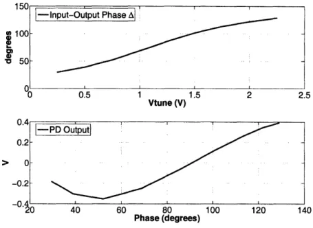
The tuning scheme takes advantage of the fact that the phase difference between filter input and filter output is 900 at the center frequency. According to eqn. (3.4),
there is a resonant condition between L and CN at the filter center frequency, where
CN = C, + Cc. This condition can be written using admittances as
1 1
w + joC = j + jwoCp + jwoCc = 0 (3.16)
jwoL
jwoL
The admittance of each resonator, consisting of L and C,, at the filter center frequency is then
Yesonator = +