HAL Id: hal-01900001
https://hal.archives-ouvertes.fr/hal-01900001
Submitted on 20 Oct 2018
HAL is a multi-disciplinary open access
archive for the deposit and dissemination of
sci-entific research documents, whether they are
pub-lished or not. The documents may come from
teaching and research institutions in France or
abroad, or from public or private research centers.
L’archive ouverte pluridisciplinaire HAL, est
destinée au dépôt et à la diffusion de documents
scientifiques de niveau recherche, publiés ou non,
émanant des établissements d’enseignement et de
recherche français ou étrangers, des laboratoires
publics ou privés.
Contrasted electronic properties of Sn-adatom-based ( 3
x 3 ) R 30 ° reconstructions on Si(111)
Anne Charrier, R. Pérez, F. Thibaudau, J.-M. Debever, J. Ortega, F. Flores,
Jean-Marc Themlin
To cite this version:
Anne Charrier, R. Pérez, F. Thibaudau, J.-M. Debever, J. Ortega, et al.. Contrasted electronic
properties of Sn-adatom-based ( 3 x 3 ) R 30 ° reconstructions on Si(111). Physical Review B:
Condensed Matter and Materials Physics (1998-2015), American Physical Society, 2001, 64 (11),
�10.1103/physrevb.64.115407�. �hal-01900001�
Contrasted electronic properties of Sn-adatom-based
„冑
3
Ã
冑
3
…R30° reconstructions on Si„111…
A. Charrier,1,*R. Pe´rez,2 F. Thibaudau,1J.-M. Debever,1J. Ortega,2F. Flores,2 and J.-M. Themlin1
1Groupe de Physique des Etats Condense´s, Faculte´ des Sciences de Luminy, Universite´ de la Me´diterrane´e,
Case 901, 13288 Marseille Cedex 9, France
2Departamento de Fı´sica Teo´rica de la Materia Condensada, Facultad de Ciencias, Universidad Auto´noma de Madrid,
Madrid 28049, Spain
共Received 17 January 2001; revised manuscript received 6 April 2001; published 23 August 2001兲 We have investigated the electronic structure of the two-dimensional solid solution SixSn1⫺x/Si(111)-(
冑
3⫻
冑
3)R30° at room temperature, with a particular emphasis on the empty states, using both global 关k//-resolved inverse photoemission spectroscopy共KRIPES兲兴 and local probes 共scanning tunneling microscopyand spectroscopy, STM and STS兲, as well as DFT-LDA calculations. This adatom overlayer with a (
冑
3 ⫻冑
3)R30° symmetry shows drastic evolution with increasing Sn-adatom concentration, including a semicon-ductor to metal transition. The Si0.5Sn0.5/Si(111)-冑
3 or mosaic phase has a single empty surface statelocal-ized at 0.56 eV above EFat⌫¯. With an overall bandwidth of ⬇0.15 eV, this spz-type state localized on Si adatoms does not cross EF: the mosaic phase is semiconducting, with a bandgap between 0.3 and 0.5 eV. This phase is characterized by a large corrugation of 0.75 Å with Sn adatoms higher than Si adatoms. In the Sn-rich limit SixSn1⫺x/Si(111)-
冑
3 with x⭐0.05, we follow an empty state U1⬘throughout most of the surfaceBril-louin zone except near the K¯ point where it clearly crosses the Fermi level. A second, empty surface state U2⬘
is detected 1.67 eV above EF. Once correlation effects suggested by the small bandwidth of U1⬘are adequately
taken into account, we explain our KRIPES results in the framework of a dynamical fluctuations model as originating from an underlying (3⫻3) structure. Finally, results pertaining to intermediate Sn-adatom concen-trations are interpreted in view of the two limiting cases.
DOI: 10.1103/PhysRevB.64.115407 PACS number共s兲: 73.20.At, 71.30.⫹h, 71.27.⫹a, 79.60.Jv
I. INTRODUCTION
Adsorption of submonolayer amounts of Sn on Si共111兲 induces a wealth of reconstructions.1Among these, the (
冑
3⫻
冑
3)R30° reconstruction共hereafter called冑
3 for brevity兲, an old and familiar object in surface science, consists of a low-density adatom overlayer on top of a bulk-truncated Si共111兲,2 which can be stabilized at room temperature for a broad Sn coverage continuously varying between 1/6 and 1/3 ML.3The widely accepted description of this overlayer in-volves 1/3 ML of adatoms located at T4 sites,4
forming an hexagonal array with the
冑
3 symmetry, with one adatom per冑
3 unit cell.5 These threefold-coordinated adatoms are lo-cated at T4sites directly above second layer substrate atomsand are bound to three atoms of the substrate first layer. However, each T4 site can accommodate either a Sn or a Si
adatom. Depending on the initial Sn coverage and annealing temperature, the overlayer can thus accommodate a wide range of compositions, and is best viewed as a purely 2D solid solution SixSn1⫺x/Si(111)-
冑
36, where a fraction (x⭐0.5) of the Sn adatoms may be substituted by isovalent Si
adatoms. Historically, the two limiting cases corresponding to x⫽0 共100% Sn兲 and x⫽0.5 have been called the␣⫺
冑
3 and ␥⫺冑
3 共or mosaic兲 phases.7 In what follows, and al-though it is understood that they are just the limiting cases of a single phase, we will be using the notation ␣⫺冑
3 and␥⫺
冑
3 and we will refer to these particular cases as if they were distinct phases. Furthermore, it should also be stressed that the ideal SixSn1⫺x/Si(111)-冑
3 (x⫽0) cannot bepre-pared at room temperature since a number of Si
substitu-tional defects is always present: x has therefore a lower prac-tical bound of the order of 0.03.
As far as the electronic structure is concerned, with a single tetravalent adatom per unit cell, it would be expected that the
冑
3 reconstruction keeps a metallic character for all Sn coverages, since three electrons are involved in the cova-lent bonding with the substrate and one electron remains in the Sn or Si adatom dangling bond. On the basis of simple electron counting rules, we expect a single metallic surface state crossing EF, derived from the s pz-like orbitalslocal-ized on each adatom.8However, this is far to be the case for the␥⫺
冑
3, obtained at a coverage of 1/6 ML of Sn共x⫽0.5兲.9 The ␥⫺冑
3, also called mosaic phase and its characteristic kinked lines were first discovered on the Sn/Si(111)-冑
3 interface10,11 and then observed on the Pb/Si共111兲 system.12 On Pb/Si(111)-冑
3, Karlsson et al.13 have evidenced a charge transfer from Si adatoms to Pb adatoms. Later, scan-ning tunneling microscopy共STM兲 measurements9,14revealed the same behavior for Sn/Si. Such a charge transfer induces the presence of two surface states, above and below the Fermi level, and the surface is semiconducting. However, the experimental and theoretical evidence reporting the exis-tence, position, overall bandwidth and dispersion of these states is still scarce, especially for the unoccupied states. Early angle-resolved photoemission15 and inverse photoemission16,17 on Sn/Si(111)-冑
3 which do show two distinct states and no obvious Fermi level crossing concluded however to a metallic character. Furthermore, the latter re-sults being anterior to the first report of the mosaic phase, it is not clear on which type of冑
3 the experiments applied, either the mosaic, the alpha phase or an intermediate. WePHYSICAL REVIEW B, VOLUME 64, 115407
have measured the unoccupied state of the mosaic phase and its detailed dispersion using k//-resolved inverse
photoemis-sion spectroscopy. As expected, this state does not cross the Fermi level, and scanning tunneling spectroscopy 共STS兲 measurements confirm that the surface is semiconducting, in good agreement with our theoretical calculations.
As additional Sn adatoms are added to the overlayer, SixSn1⫺x/Si(111)-
冑
3 (x⬍0.5) should undergo asemicon-ductor to metal transition, since the host (x⬇0) ␣⫺
冑
3 phase, which can be stabilized at room temperature, only contains Sn adatoms 共at a coverage of 1/3 ML兲. The avail-ability of a single site clearly prevents any charge transfer, and the reconstruction, at first sight, should be metallic. However, we are still missing a clear spectroscopic evidence of the Fermi level crossing for ␣⫺冑
3. We will show that most of this ‘‘metallic’’ s pz-adatom derived state is indeed unoccupied and can be followed in a large portion of the reconstructed surface Brillouin zone共SBZ兲. The Fermi level crossing is clearly visible in the immediate vicinity of the K¯ point, where the state disappears from the angle-resolved KRIPES spectra. The overall bandwidth of this state is small, of the order of 0.55 eV, so correlation effects are expected to play a role.There are, however, some additional puzzling results. While the above-described picture of the ␣⫺
冑
3 phase readily accounts for a single metallic surface state, we have observed a second empty surface state 1.67 eV above the Fermi level. This observation is not compatible with the ex-istence of a single T4site, but rather suggests that more thanone site is involved in the actual structure of the ␣⫺
冑
3 phase. This has already been suggested by previous photo-emission studies18 which have shown that the Sn 4d core level intriguingly contains two components. Similar results have been observed for the closely related Sn/Ge共111兲 system.19,20In this case, the room-temperature共RT兲 ␣⫺冑
3 phase undergoes a structural phase transition at low tempera-ture to a 3⫻3 phase.21 On the basis of first-principles mo-lecular dynamics simulations, this transition has been interpreted19 in terms of a dynamical fluctuations model in which fluctuating adatoms at room temperature, are stabi-lized in a 3⫻3 phase at low temperatures. Surface x-ray diffraction studies22,23and DFT-LDA calculations19,24 show that the low temperature phase is a 3⫻3 reconstruction with two different types of Sn adatoms, both on T4 sites, but one⬃0.3 Å higher than the other. This low-temperature phase
has also been proposed to correspond to the formation of a charge density wave.21Some recent results indicate that Sn/ Si共111兲 should also exhibit such atomic fluctuations,25 al-though no 3⫻3 phase is expected to appear at low temperature.26,27 Based on this fluctuations model, our KRIPES data receive a natural explanation provided that cor-relation effects are properly taken into account. Finally, re-sults pertaining to intermediate phases are interpreted in view of the two limiting cases.
II. EXPERIMENTAL PROCEDURES
KRIPES experiments were performed in an ultrahigh-vacuum chamber 共base pressure 3⫻10⫺10 mbar) equipped
with a low-energy electron diffractometer 共LEED兲 and an inverse photoemission setup.28The latter consists of an elec-tron gun and an elliptical mirror to focus photons emitted in a large solid angle towards the photon detector. The Geiger-Mu¨ller type detector filled with a helium-iodine mixture and sealed with a SrF2 window operates in an isochromat mode at a fixed photon energy of 9.5 eV. The overall energy reso-lution, determined by measuring the Fermi edge on a Ta foil, is 0.35 eV, including the electron gun and the detector. The dispersion within the surface Brillouin zone共SBZ兲 of interest is investigated by rotating the electron gun in a vertical plane perpendicular to the sample surface 共variable polar angle with respect to the surface normal兲 and oriented along a given azimuth.
STM and STS experiments were performed in an ultra-high vacuum chamber equipped with an OMICRON system
共base pressure 1⫻10⫺10 mbar) and a tungsten tip. The
typi-cal setpoint current used to obtain STM images and STS measurements were, respectively, 50 and 100 pA. STS re-sults represent an average over the surface obtained with 47 measurements, each of them being taken with an acquisition time of 50 ms.
We used phosphorus-doped 共resistivity ⬃2
⫻10⫺2 ⍀ cm) Si共111兲 wafer samples of size 20⫻5
⫻0.28 mm3. Before introducing into vacuum, the sample is
chemically prepared ex situ by a wet hydrogenation proce-dure. In the KRIPES setup, the sample is then annealed in UHV by electron bombardment on its reverse side using a BaO cathode. In the STM case, annealing is performed by direct Joule heating. The annealing temperature was moni-tored by an infrared pyrometer assuming an emissivity of 0.8.29 The starting point before evaporation of Sn was the 7⫻7 reconstruction obtained by annealing the Si sample around 1200°C.
冑
3 phases are obtained by the deposition of approximately 1.5 ML of Sn at RT. The surface is then an-nealed at 630 °C during 2 min for the ␣⫺冑
3 phase, 4 min-utes for the ␥⫺冑
3 phase, and between 2 and 4 minutes for the intermediate phases. The orientation and surface quality of every surface reconstruction was checked by LEED.III. STM RESULTS
One of the most difficult part of this work was the prepa-ration of the appropriate surface, since markedly different reconstructions with very similar
冑
3⫻冑
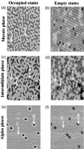
3 symmetry and the same diffraction pattern may be prepared for the Sn/Si共111兲 interface. Within the adatom layer, a continuum of Sn ada-tom concentrations can be obtained between two limits of 1/6 ML 共the ␥ or mosaic phase兲 and 1/3 ML of Sn 共the ␣ phase兲.In order to calibrate our preparation procedure and to un-derstand the differences between these phases, we have real-ized a scanning tunneling microscopy study for both␣ and␥ phases as well as for intermediate cases. Figures 1共a兲–1共f兲 shows STM images of three phases. Images共a兲 and 共b兲 were obtained on the mosaic phase at, respectively,⫺1 V
共occu-pied states兲 and 1 V 共empty states兲; 共c兲 and 共d兲 represent an intermediate phase at ⫺0.45 and 0.45 V and finally 共e兲 and
共f兲 are images obtained on the␣ phase at⫺0.45 and 0.45 V. The three sets of images obtained for each phase are very different. Three types of adatom sites can be observed on this image as indicated in Table I.
The mosaic phase关Figs. 1共a兲 and 1共b兲兴 is known to con-tain an equal amount of Sn and Si adatoms.9The possibility of a charge transfer between Sn and Si adatoms is neglected in a first approach; they are both tetravalent and share the same electronegativity. Since all the adatoms are bound to
three atoms of the outermost Si layer, their dangling bond should hold one electron. The density of occupied and empty states observed in the STM images is thus expected to be quite homogeneous over the surface. Although this is the case in the empty states,30two types of protrusions共A and B兲 are seen in the occupied states 关Fig. 1共a兲兴. An estimation of the amount of the protrusions for these two families indicates the presence of about 50% of each. Each family of protru-sions must correspond to either Sn or Si adatoms.
Can we explain this large intensity difference on the sole basis of structural arguments? The covalent radius of Sn
共1.40 Å兲 is larger than that of Si 共1.17 Å兲, but a cross section
of the occupied state indicates a corrugation of 1.6 Å, much larger than the covalent radii difference. This implies that we can expect an important topographic corrugation with the tin atoms in a position higher than that of Si.
We have analyzed the adatom geometry corresponding to the mosaic phase, using a first-principles DFT-LDA tight-binding molecular dynamics technique.31 In these calcula-tions we have assumed, for the sake of simplicity, a 2
冑
3⫻
冑
3 geometry with one Sn adatom and one Si adatom per surface unit cell. Four Si layers are included in the calcula-tion, and the lower one is saturated by H atoms. We find that, once the atomic positions are relaxed to their minimum en-ergy configuration, the Sn adatoms are higher than Si ada-toms by⬃0.75 Å . The total corrugation seen in STM, i.e., 1.6 Å, is larger than this physical corrugation plus the differ-ence of the covalent atomic radii (⬃0.23 Å ): this can be ascribed to the electron charge transfer from Si to Sn asso-ciated with the formation of a semiconductor gap at EF.Figure 2 shows the electronic band structure for this surface
关Si0.5Sn0.5/Si(111)-2
冑
3⫻冑
3兴. Our calculations show anen-ergy gap of 0.25 eV between Sn-like filled states and Si-like empty states.
As the amount of tin is slightly increased, intermediate phases can be observed, such as the one shown in Figs. 1共c兲 and 1共d兲. In addition to the A- and B-type protrusions of the mosaic phase, we observe a C-type adatom site and the total
FIG. 1. STM images obtained on three phases of SixSn1⫺x/Si(111)⫺
冑
3. 共a兲 and 共b兲 show images of the mosaic phase (x⯝0.5) respectively obtained at -1 V 共occupied states兲 and 1 V 共empty states兲. 共c兲 and 共d兲 represent the intermediate phase at -0.45 V and 0.45 V.共e兲 and 共f兲 are images of the␣ phase (x⯝0) at ⫺0.45 and 0.45 V. Images of the intermediate and alpha phases have been taken simultaneously at the same location.TABLE I. Different types of adatom sites observed on the mo-saic, intermediate, and␣ phases.
Mosaic Intermediate Alpha
Occupied Empty Occupied Empty Occupied Empty Type A Bright Dark Bright Dark
Type B Dark Dark Dark Dark Dark Dark
type C Bright Bright Bright Bright
FIG. 2. Surface band structure along the symmetry directions M⬘-⌫-K⬘-M⬘of the SBZ for Sn/Si(111)⫺(2
冑
3⫻冑
3) with one Sn adatom and one Si adatom, simulating the mosaic structure. The lower 共occupied兲 surface band is associated with the Sn dangling bond while the upper 共empty兲 surface band is related to the Si dangling bond. The energy of these bands is indicated with respect to the Fermi level. The surface is semiconducting.CONTRASTED ELECTRONIC PROPERTIES OF Sn- . . . PHYSICAL REVIEW B 64 115407
number of white protrusions is increased in both occupied and empty states with respect to the mosaic phase. In the occupied states, these white protrusions must thus corre-spond to Sn adatoms and the charge transfer occurs from Si adatom towards Sn adatom,7 in agreement with the LDA calculations mentioned above. This charge transfer perfectly explains the mosaic images; the large difference in density of states is accentuated at ⫺1 V and compensated at 1V 共in terms of intensity兲 by the difference in heights between Sn and Si adatoms.
In the intermediate phase, this charge transfer cannot in-volve all the Sn adatoms since there are more Sn than Si adatoms. That makes the difference between A and C types of Sn adatoms. The A-type adatoms still make the charge transfer and have a fully occupied DB while the C-type Sn adatoms remain with a half-filled DB. The latter appear white in both occupied and empty states共we will see below that these half-filled DB have to be understood as the aver-age of the DB occupancies associated with height-fluctuating adatoms兲. The dark protrusions in the empty states are attrib-uted to Si (B-type兲 and A-type Sn adatoms. The reason why the Si adatoms with empty DBs appear dark is related to their location (⬃0.5 Å below the Sn adatoms with half-occupied DBs兲 which reduces the Si adatom contribution to the STM image.
The␣ phase关Figs. 1共e兲 and 1共f兲兴 mainly contains C-type Sn adatoms (⭓97%) and a few defects (⭐3% of substitu-tional Si adatoms, B type兲. The brightest protrusions around the defects have recently been interpreted in terms of a localized 3⫻3 periodicity stabilized around the defects at RT.26
IV. THE␣-
冑
3 PHASEFigures 3共a兲 and 3共b兲 shows KRIPES results measured on the␣ phase. These spectra were obtained along the two high-symmetry directions⌫K
⬘
and⌫M⬘
of the reconstructed sur-face Brillouin zone, for various polar angles of the incident electron beam on one side of the surface normal for each azimuth. These spectra give the number of detected photons共normalized to the incident current on the sample兲 versus the
electron energy with respect to the Fermi level (EF). In order to find the positions of the different empty states, a back-ground line is removed from the raw data 共dots兲 and the spectra is then fitted with a set of Gaussians. The final fit is given by a continuous line. The maximum of each Gaussian, marked by a vertical bar, indicates the presence of an empty state. A set of five Gaussians was necessary to fit the spectra, indicating the presence of five different states. In both direc-tions ⌫K
⬘
and ⌫M⬘
, the intensity of the first two states is maximum at normal incidence 共the SBZ center is probed兲 and decreases as the angle of incidence of the electrons in-creases 共the SBZ edge is probed兲 while the intensity of the upper states remains almost unchanged for every angle. All these states can be followed along the ⌫M⬘
direction, and therefore do not cross EF along this azimuth. Along the⌫K⬘
direction, the four upper states are followed all over the SBZ whereas the lower one approaches EF as the polar angle
increases and finally disappers around 30° (k//⯝0.6 Å⫺1).
This Fermi level crossing gives a metallic character to the surface.
This metallic nature has been confirmed by scanning tun-neling spectroscopy 共STS兲 关Fig. 4共a兲兴; this spectrum gives the current intensity crossing the surface versus the voltage applied to the tip. The current-voltage characteristic is linear at these low voltages, a typical result for STS of metals. This STS curve has not been taken over a single adatom site but rather represents the average behavior of the surface.
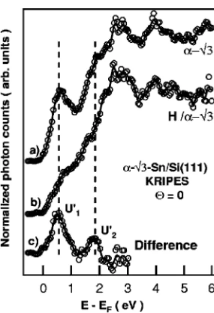
The determination of the origin of the observed states requires further experiments, since each state can be inter-preted as surface states, surface resonances or bulk states. A simple experiment consists in saturating the dangling bonds without modifying the surface reconstruction by exposure to atomic hydrogen, obtained through dissociation of the mol-ecule by a nearby hot filament. Figure 5 shows spectra of the
␣ phase under the same conditions 共a兲 before and 共b兲 after exposure at⌫¯. After exposure, the intensity decrease mainly
FIG. 3. KRIPES spectra of the␣⫺
冑
3 surface along the⌫K⬘共a兲 and⌫M⬘共b兲 directions of the SBZ for selected angles of the inci-dent electrons. Experimental curves are plotted as circles, the fit is represented by a continuous line, and each Gaussian maximum is marked by a vertical bar.FIG. 4. STS measurements of the␣ 共a兲 and mosaic 共b兲 phases. We used a typical setpoint of 100 pA and the spectra represent an average over the surface obtained from 47 measurements.
concerns U1
⬘
and U2⬘
. This decrease is emphasized inspec-trum 共c兲, the difference between the two previous spectra which reveals the adsorption-sensitive surface states共the re-versibility of this procedure by heating indicates the conser-vation of the surface reconstruction during hydrogenation兲. The higher three energy states which remain unaffected by the hydrogen are interpreted as bulk states. The surface states
U1
⬘
and U2⬘
are, respectively, found at 0.58 and 1.67 eVabove EF at⌫¯.
Figure 6 shows the band dispersion of the different states, i.e., the electron energy versus the wave-vector projected parallel to the surface. Results obtained with positive and negative angles, i.e., from both sides of surface normal for a given azimuth have been superimposed. The shape of the
band dispersions of U1
⬘
and U2⬘
, which shift towards EF when approaching the SBZ edges is characteristic of a pzadatom derived surface state.8,32 Moreover, Nicholls et al.33 have shown that for adatoms in T4 sites, substrate atom
or-bitals with wave vectors near the edges of the 1⫻1 SBZ couple favorably to the adatom states, giving rise to an oc-cupied state, while those with wave vector near the 1⫻1 SBZ center give rise to empty states. Thus, in the empty states, we expect a high intensity near⌫¯ which decreases as we approach the SBZ edges. Although our KRIPES spectra have been taken up to 40° only, the behavior of the intensity of the first peak is in good agreement with this theory 共the 1⫻1 SBZ edge corresponds to about 50°). We thus conclude that U1
⬘
and U2⬘
are adatom-derived surface states. Moreover, since the ␣-冑
3 phase contains more than 97% of Sn ada-toms, both of these states are characteristic of Sn. We also notice that their band dispersions are similar, although the bandwidth of U2⬘
(W2⫽0.4 eV) is smaller than that ofU1
⬘
(W1⭓0.58 eV).The ␣-
冑
3 reconstruction is usually described with a single Sn adatom per unit cell, with one electron per adatom dangling bond. This model is seriously questioned by the existence of two empty surface states U1⬘
and U2⬘
, a result that suggests the presence of more than one type of adatom in this surface. The existence of at least two types of adatom sites for this phase has also been suggested by Sn 4d core level measurements18,34,35 which reveal the presence of at least two components.Similar results have been observed on the Sn/Ge共111兲 interface19,20 across the reversible
冑
3⫻冑
3R30°↔3⫻3 phase transition using core level and valence-band photo-emission spectroscopies. They found, both below and above the transition, two components in the Sn 4d core level and two occupied surface states, one of them crossing the Fermi level. Theoretical calculations19,24 show that these two ef-fects are due to the existence of two structurally different types of Sn adatoms in the ground state of the system 共the 3⫻3 reconstruction兲, both on T4 sites but one ⬃0.3 Åhigher than the other. The ‘‘up’’ adatoms present fully occu-pied DBs共occupancy ⫽ 1兲 while the remaining electron 共per 3⫻3 unit cell兲 is shared by two ‘‘down’’ DBs 共occupancy ⫽ 1/4兲.24 It has been recently shown that the
冑
3⫻冑
3↔3⫻3 phase transition in Sn/Ge共111兲 is associated with a surface soft phonon27where the Sn adatoms display at RT correlated up/down vibrations with large amplitudes, keeping memory of the underlying 3⫻3 phase. These dynamical fluctuations19explain the two components in the Sn 4d core level and the two occupied surface states observed for the␣-
冑
3 phase.The Sn/Si共111兲 system does not display the ␣–
冑
3↔3⫻3 transition,26 since the
冑
3 is the stable structure at lowT.27Nevertheless, the atomic motion at RT is similar to the Sn/Ge case, since the vibration associated with the 3⫻3 structure is a minimum of the surface phonon dispersion and the atomic motion should be dominated by this mode.27 In other words, the soft phonon responsible for the ␣–
冑
3↔3⫻3 transition in Sn/Ge is partially softened in the Sn/Si case,
explaining the similarities of both cases at RT; in particular, the Sn/Si(111)-␣-
冑
3 electronic structure is also determinedFIG. 5. 共a兲 and 共b兲 KRIPES spectra of the␣ phase respectively obtained before and after exposure of the sample to 1L of atomic hydrogen.共c兲 Difference curve 共a兲,共b兲.
FIG. 6. Unoccupied band dispersions E(k//) of the ␣ phase.
Electron energy is plotted against the wave vector parallel to the surface.
CONTRASTED ELECTRONIC PROPERTIES OF Sn- . . . PHYSICAL REVIEW B 64 115407
by locally fluctuating ‘‘3⫻3’’ atomic geometries.
In order to understand the electronic properties of the Sn/Si(111)-␣-
冑
3 surface, and in particular its unoccupied surface bands, we have to analyze the electronic structure of the underlying 3⫻3 geometries. At RT the Sn adatoms vi-brate between ‘‘up’’ and ‘‘down’’ positions 共see Ref. 27兲 which differ by⌬z⬃0.3 Å ; thus, the electronic structure of a Sn/Si(111)-3⫻3 surface, with ⌬z⬃0.3 Å has been analyzed.36 The LDA result shows a fully occupied surface band ⬃0.15 eV below EF, and two overlapping surface bands at EF with a bandwidth of W⬃0.3 eV and anoccu-pancy of 1/4共i.e., one electron for two bands兲. The effective intrasite coulomb interaction Ueff for the Sn-dangling bonds
is estimated to be Ueff⫽1.15 eV,36 i.e., UeffⰇW and
elec-tron correlation effects have to be considered. Figure 7共a兲 schematically shows how the LDA band at EF is changed
when introducing electron correlations: the effect of Ueffis to create a new state at EF⫹Ueff, with 1/4th of the initial
weight, while the weight of the state that remains at EF is
reduced by 3/4 共i.e., three electrons per 3⫻3 unit cell兲. This theoretical analysis, including many-body effects, is in very good agreement with the experimental KRIPES re-sults: the band at EF is identified with U1
⬘
, while the band atEF⫹Ueffperfectly explains the U2
⬘
state. Moreover, thedif-ference in energy of the two empty surface states, 1.1 eV, is very close to the theoretical result Ueff⫽1.15 eV. This good
agreement between experimental and theoretical results for the unoccupied surface bands provides a strong support to the interpretation of the Sn/Si(111)-␣-
冑
3 surface as a dy-namically fluctuating phase in which, at RT, the atomic mo-tion is dominated by a 3⫻3 surface phonon.27In Sec. VI, an independent confirmation of the weight of U1⬘
will support the present interpretation further. We also mention that if the Sn adatoms are assumed to be at the same height on the surface, one would expect for the surface electronic structure a Mott-Hubbard transition as in the case of SiC-冑
3 共Ref. 32兲 and the surface should be semiconducting关see Fig. 7共b兲兴, in disagreement with the experimental evidence.It should be mentioned that this interpretation of the␣-
冑
3 phase is not incompatible with the relative flatness of the STM images on the ␣ phase 关Figs. 1共e兲,1共f兲兴, although the weak corrugation on these images suggests the presence of a single type of adatom site. In this model where the adatoms fluctuate, the STM acquisition time is far too slow to see these adatom fluctuations. What we observe is an average of these two adatom positions 关the Sn half-filled DB of Figs. 1共c兲,1共d兲 can also be associated with this fluctuations model兴. Conway et al. using x-ray diffraction experiments and Keating strain energy minimization have determined a single value of 1.58 Å for the Sn adatom height on Sn/Si(111)-冑
3⫻冑
3.37Apart from the fact that the detailed stoichiometry in the adatom layer is unknown in this early experiment, this value is not compatible with a mean value of more than 2 Å obtained from electron standing waves recently reported by Yamanaka and Ino, who have ques-tioned the effectiveness of the preceding method for deter-mining adatom heights above bulk atomic planes.38The best fit to these diffraction results has indeed been obtainedconsidering two kinds of Sn adatoms with a height difference of 0.3 Å.
V. THE␥ PHASE
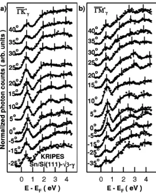
Figures 8共a兲,8共b兲 shows KRIPES spectra obtained on the
␥ phase 共mosaic phase兲 for positive and negative polar angles along the directions⌫K
⬘
and⌫M⬘
of the SBZ. A setFIG. 7. Electron correlation effects in the Sn/Si(111)-␣-
冑
3 sur-face:共a兲 3⫻3 case; 共b兲 flat冑
3⫻冑
3 case共see text兲. In 共a兲 electron correlation effects change the LDA band at EF, creating a new stateat EF⫹Ueff with 1/4th of the initial weight. The system remains
metallic. If all the Sn adatoms were equivalent 共b兲 the surface should be insulating.
of four Gaussians was required to fit these spectra in the range 0 to 5 eV above the Fermi level. The first state (U1) is
localized at 0.56 eV above EFat⌫¯ and the three others are at 1.71, 2.61, and 3.75 eV. These states disperse all over the surface Brillouin zone. In both directions⌫K
⬘
and⌫M⬘
, the intensity of U1 is maximum at normal incidence共SBZcen-ter兲 and decreases as the angle of incidence of the elec-trons increases towards the SBZ edges; conversely, the inten-sity of the upper states remains almost unchanged for all angles.
The band dispersion of these states are given in Fig. 9. The dispersion of U1 tends to get closer to EF near the SBZ
edges; it reaches 0.38 eV at K¯
⬘
, and its bandwidth is about 0.15 eV. Hence U1 does not cross EF and the surface issemiconducting. Previous ARUPS studies16,39 have shown the presence of an occupied surface state at 0.1 eV below
EF. Therefore we can estimate the band gap to be around 0.5
eV. This semiconducting character has been confirmed by STS measurements, shown in Fig. 4共b兲. This curve repre-sents an average of 47 measurements taken over the surface. On this spectrum, we observe the lack of current through the surface for applied voltage between 0 and 0.3 V indicating the presence of a gap around 0.3 eV.
The band dispersion of U1 is in good agreement with the
calculations presented above 共see Fig. 2兲 for the Si0.5Sn0.5/Si(111)-2
冑
3⫻冑
3 surface, which represents themosaic phase in a simplified way. Our DFT-LDA calcula-tions show an energy gap of 0.25 eV between Sn-like filled states and Si-like empty states, in good agreement with the STM data, and a very narrow bandwidth of 0.1 eV for the
empty states. DFT-LDA calculations, which fail to describe the excited systems, are known to underestimate band gaps in insulators. Our KRIPES and LDA data are thus systemati-cally shifted by⬇0.3 eV, suggesting that the energy gap is probably between 0.3 and 0.5 eV.
For the␥ phase, we exposed the sample to 1 L of atomic hydrogen. Figure 10 shows the spectra obtained before 共a兲 and after共b兲 exposition at ⌫¯ in the same conditions; 共c兲 is the difference between the two previous spectra. Whereas the first state intensity has nearly decreased to zero, the higher energy states are not visible in the difference signal. Hence we can conclude that U1 is a surface state and that the three
upper states correspond to bulk states. Moreover, the shape of the dispersion of U1 and its shift towards EF as we get
closer to the SBZ edges is characteristic, as for the␣ phase, of a surface state mainly derived from pz-type orbital
local-ized on the adatoms. This, in agreement with the STM and
FIG. 8. KRIPES spectra of the ␥-
冑
3 共mosaic兲 reconstruction along the directions⌫K⬘共a兲 and ⌫M⬘共b兲 of the SBZ for selected positive and negative angles of the incident electrons. The vertical bars represent the position of the maximum of each Gaussian.FIG. 9. Experimental band dispersion of the␥-
冑
3 reconstruc-tion. Electron energy is plotted against the wave vector parallel to the surface.FIG. 10. 共a兲 and 共b兲 KRIPES spectra of the ␥ phase, respec-tively obtained before and after exposure of the sample at 1L of atomic hydrogen.共c兲 Subtraction 共a兲⫺共b兲.
CONTRASTED ELECTRONIC PROPERTIES OF Sn- . . . PHYSICAL REVIEW B 64 115407
LDA results, shows that U1 is located primarily on Si adatoms.
VI. FROM THE MOSAIC TO THE␣ PHASE
Starting from the mosaic phase, we still have to explain how the surface evolves with increasing Sn coverage. Figure 11 shows four KRIPES spectra obtained at⌫¯ on the follow-ing phases: 共a兲 the mosaic phase, 共b兲 a first intermediate phase interm1 close to the mosaic;共c兲 a second intermediate
phase interm2closer to the␣phase, and共d兲 the␣phase. The
mosaic phase关Fig. 11共a兲兴 presents a single surface state U1
at 0.56 eV. According to the STM and LDA results, this state must be attributed to Si adatoms, as previously explained. The interm1phase关Fig. 11共b兲兴 evidences three surface states
U1
⬘
, S2 and U2⬘
. These three states are also present oninterm2 关Fig. 11共c兲兴. However, the S2 peak decreases when
the Sn concentration increases while U1
⬘
and U2⬘
become more intense. In conclusion, the intensity of S2follows the Siadatom concentration; S2 is thus associated with Si adatoms.
Therefore, S2and U1correspond to the same state. A similar
argumentation confirms the attribution of U1
⬘
and U2⬘
to Sn adatoms. This interpretation is confirmed by the behavior of the ␣ phase关Fig. 11共d兲兴 where these three peaks follow the same evolution. If the ␣ phase was perfect, the S2 peakwould completely disappear. The weak residual intensity seen on Fig. 11共d兲 must be attributed to the few substitutional Si adatoms considered here as defects.
In order to identify theoretically the isolated Si-defect level 关S2 peak in Fig. 11共d兲兴 we have also calculated a Si impurity in a Sn/Si⫺3⫻3 reconstruction. Without going into details, we only mention here that the Si-induced level is located around 0.2 eV above EF, higher than U1
⬘
, in goodagreement with the experimental data 共taking into account the systematic shift between experimental and theoretical data mentioned above兲.
The first structures near EF in Fig. 11关U1
⬘
and S2in Figs. 11共b兲–11共d兲, or peak U1in Fig. 11共a兲兴 have a global decreas-ing area when the amount of tin increases. This change in intensity is explained by the density of electrons in the bands. Although the adatom electronic density has not changed, their nature is different. In the case of the mosaic phase关Fig. 11共a兲兴, two types of adatoms are present, Sn and Si, giving rise to two bands. As discussed above, the Sn-DB band is completely filled, while the Si-DB band is com-pletely empty; therefore, the density of unoccupied states in the Si-band (U1) is 1 electron per冑
3 unit cell. In the case of a perfect ␣ phase 关Fig. 11共d兲兴, the state U1⬘
presents a totaldensity of states of 3/4⫻ 4 ⫽ 3 electrons per 3⫻3 unit cell
共see Sec. IV兲; this state is occupied by 1 electron 共per 3⫻3
unit cell兲, leaving a density of unoccupied states of 2/3 of electron per
冑
3 unit cell关see also Fig. 7共a兲兴.36The height of the U1
⬘
peak on the␣ phase is accordingly lower than the one of U1 on the ␥ phase. The density ofelectron attributed to each band is thus directly correlated to the peak areas, itself correlated to the stoichiometry of the surface. The area of the first two peaks for the two interme-diate phases关Figs. 11共b兲,11共c兲兴 is in between the␣ and mo-saic ones. This stoichiometry can be determined by two dif-ferent methods based on the individual component areas. In order to account for the finite surface state dispersion, an effective area has been calculated based on the peak intensity times the Gaussian FWHM for normal incidence artificially augmented by the overall bandwidth of the state. The first method consists in normalizing the area of the Si derived Gaussian (S2) with a reference of known Si concentration
similar to the spectrum obtained on the mosaic phase 关we consider a perfect mosaic phase Fig. 11共a兲, where A1, the U1 Gaussian area corresponds to 50% of Si adatoms兴. This method gives x, the concentration of Si adatoms, from which we deduce the Sn concentration (1⫺x). In the second method, the Sn (U1
⬘
) and Si (S2) Gaussian areas of a unique spectrum, respectively called ASn and ASi, are normalized by their sum (ASn⫹ASi). Before doing this calculation, eachGaussian area is normalized by the electron weight, i.e., 2/3 for Sn (U1
⬘
) and 1 for Si (S2). Figure 12 compares therela-tive concentration of Si adatoms found for the three phases,
␣, interm2, and interm1 of Figs. 11共d兲, 11共c兲, 11共b兲, obtained by the two methods. The results obtained are very close to the ideal correspondance line. These calculations thus con-firm our interpretation which attributes a weight of 2/3 of electrons on the U1
⬘
component. On the basis of the relative weights of the components which have been attributed to Si and Sn adatoms, it is thus possible to deduce the relative concentrations of both species in the adatom layer from a single inverse photoemission spectrum.We finally notice a shift towards the higher energies of the bulk states as the amount of tin is increased. This is attrib-uted to a band bending effect.
VII. SUMMARY AND CONCLUSIONS
In this work, we have presented a detailed study of the electronic structure of Sn/Si共111兲-(
冑
3⫻冑
3)R30° system atFIG. 11. KRIPES spectra obtained at normal incidence for 共a兲 the ␥ phase, 共b兲 the intermediate phase close to the mosaic phase 共interm1兲, 共c兲 an intermediate phase close to the␣ phase, and 共d兲 the␣ phase.
submonolayer coverages of Sn, with a particular emphasis on the unoccupied states. The electronic structure of the 2D solid solution SixSn1⫺x/Si(111)⫺(
冑
3⫻冑
3)R30° at roomtemperature has been studied by global共KRIPES兲 and local
共STM, STS兲 probes, as well as by DFT-LDA calculations.
Depending on the Sn coverage between 1/6 and 1/3 ML, the adatom overlayer with a (
冑
3⫻冑
3)R30° symmetry shows contrasting electronic properties, including a semiconductor to metal transition. The Si0.5Sn0.5/Si(111)-冑
3 or mosaicphase has a single empty surface state localized at 0.56 eV above EFat⌫¯. With an overall bandwidth of ⬇0.15 eV, this s pz-type state localized on Si adatoms does not cross EF:
the mosaic phase is semiconducting, with a bandgap between 0.3 and 0.5 eV. This phase is characterized by a large corru-gation of 0.75 Å with Sn adatoms higher than Si adatoms. In the Sn-rich limit SixSn1⫺x/Si(111)-
冑
3 with x⭐0.05, wefol-low an empty state U1
⬘
throughout most of the surface Bril-louin zone 共SBZ兲 except near the K¯ point where it clearly crosses the Fermi level. A second, empty surface state U2⬘
is detected 1.67 eV above EF. Once electron correlation effects are adequately taken into account, we explain our KRIPES results for the ␣ phase as originating from an underlying (3⫻3) atomic geometry which is dynamically fluctuating at RT. These fluctuations are attributed to an incomplete soft-ening of a surface phonon.27ACKNOWLEDGMENTS
This work has been partially funded by the spanish CICYT under Project No. PB97-0028.
*Corresponding author: [email protected]
1T. Ichikawa, Surf. Sci. 140, 37共1984兲.
2D.T. Wang, N. Esser, M. Cardona, and J. Zegenhagen, Surf. Sci.
343, 31共1995兲.
31ML is defined as one metal atom for one Si atom of the first
Si共111兲 layer which corresponds to a density of 7.84 1014 atoms/cm2.
4J.M. Nicholls, B. Reihl, and J.E. Northrup, Phys. Rev. B 35, 4137
共1987兲.
5C.A. Sebenne, Surface Physics and Related Topics, edited by
Fu-Jia Yang et al.共World Scientific, Singapore, 1991兲, p. 259.
6J.M. Carpinelli, H.H. Weitering, and E. W. Plummer, Surf. Sci.
401, L457共1998兲.
7G. Le Lay, J. Phys. IV 7, 115共1997兲.
8J.E. Northrup and J. Neugebauer, Phys. Rev. B 52, R17001
共1995兲.
9C. To¨rnevik, M. Go¨thelid, M. Hammar, U.O. Karlsson, N.G.
Nils-son, S.A. Flodstro¨m, C. Wigren, and M. O¨ stling, Surf. Sci. 314, 179共1994兲.
10J. Nogami, Sang-il Park, and C.F. Quate, J. Vac. Sci. Technol. A 7,
1919共1989兲.
11J.A. Kubby, Y.R. Wang, and W.J. Greene, Phys. Rev. Lett. 65,
2165共1990兲.
12E. Ganz, F. Xiiong, I.-S. Hwang, and J. Golovchenko, Phys. Rev.
B 43, 7316共1991兲.
13C.J. Karlsson, E. Landemark, Y.-C. Chao, and R.I.G. Uhrberg,
Phys. Rev. B 45, 6321共1992兲.
14X.F. Lin I. Chizhov, H.A. Mai, and R.F. Willis, Surf. Sci. 366, 51
共1996兲.
15T. Kinoshita, S. Kono, and T. Sagawa, Phys. Rev. B 34, 3011
共1986兲.
16T. Kinoshita, H. Ohta, Y. Enta, Y. Yaegashi, S. Suzuki, and S.
Kono, J. Phys. Soc. Jpn. 56, 4015共1987兲.
17H. Ohta, T Kinoshita, Y. Yaegashi, S. Suzuki, and S. Kono, J.
Phys. Soc. Jpn. 57, 4432共1988兲.
18M. Go¨thelid, M. Bjo¨rkqvist, T.M. Grechk, G. Le Lay, and U.O.
Karlsson, Phys. Rev. B 52, R14352共1995兲.
19J. Avila, A. Mascaraque, E.G. Michel, M.-C. Asensio, G. Le Lay,
J. Ortega, R. Pe´rez, and F. Flore´s, Phys. Rev. Lett. 82, 442 共1999兲.
20R.I.G. Uhrberg and T. Balasubramanian, Phys. Rev. Lett. 81,
2108共1998兲.
21J.M. Carpinelli, H.H. Weitering, M. Bartkowiak, R. Stumpf, and
E.W. Plummer, Phys. Rev. Lett. 79, 2859共1997兲.
22O. Bunk et al., Phys. Rev. Lett. 83, 2226共1999兲.
23J. Zhang, Ismail, P.J. Rous, A.P. Baddorf, and E.W. Plummer,
Phys. Rev. B 60, 2860共1999兲.
24
J. Ortega, R. Pe´rez, and F. Flores, J. Phys.: Condens. Matter 12, L21共2000兲.
25Sleza´k, P. Mutambo, and V. Cha´b, Phys. Rev. B 60, 13328共1999兲. 26L. Ottaviano, M. Crivellari, L. Lozzi, and S. Santucci, Surf. Sci.
445, L41共2000兲.
27R. Pe´rez, J. Ortega, and F. Flores, Phys. Rev. Lett. 86, 4891
共2001兲.
28S. Bouzidi, F. Coletti, J.-M. Debever, P.A. Thiry, P. Dumas, and Y.
Chabal, Phys. Rev. B 45, 1187共1992兲.
29P.J. Timans, J. Appl. Phys. 74, 6353共1993兲.
30Remaining differences may be ascribed to the markedly different
sizes of Sn and Si adatoms.
31A.A. Demkov, J. Ortega, O.F. Sankey, and M.P. Grumbach, Phys.
Rev. B 52, 1618共1995兲; O.F. Sankey and D.J. Niklewski, ibid. 40, 3979共1989兲.
FIG. 12. Si concentration calculated from Figs. 11共b兲–11共d兲 spectra with two different methods: x1, first method and x2, second
method. See text for a description 共Sec. IV兲 of the methods. The concentration x2has been obtained with a relative weight of 2/3 for
the electronic densities of U1⬘ 共Sn derived兲 with respect to S2 共Si
derived兲.
CONTRASTED ELECTRONIC PROPERTIES OF Sn- . . . PHYSICAL REVIEW B 64 115407
32J.-M. Themlin, I. Forbeaux, V. Langlais, H. Belkhir, and J.-M.
Debever, Europhys. Lett. 39, 61共1997兲.
33J.M. Nicholls, P. Ma˚rtensson, G.V. Hansson, and J.E. Northrup,
Phys. Rev. B 32, 1333共1985兲.
34G. Le Lay, J. Janski, P.O. Nilsson, and U.O. Karlsson, Appl. Surf.
Sci. 56Õ58, 178 共1992兲.
35H.T. Anyele, C.L. Griffiths, A.A. Caffola, C.C. Matthai, and R.H.
Williams, Appl. Surf. Sci. 123Õ124, 480 共1998兲.
36A. Charrier, R. Pe´rez, F. Thibaudau, J.-M. Debever, J. Ortega, F.
Flores, and J.-M. Themlin, J. Phys. Condens. Matter 13, L521 共2001兲.
37K.M. Conway et al., Surf. Sci. 215, 555共1989兲.
38T. Yamanaka and S. Ino, Phys. Rev. B 61, R5074共2000兲. 39C. Karlsson, Y.-C. Chao, E. Landemark, and R.I.G. Uhrberg