HAL Id: hal-01921215
https://hal.archives-ouvertes.fr/hal-01921215
Submitted on 27 May 2019HAL is a multi-disciplinary open access archive for the deposit and dissemination of sci-entific research documents, whether they are pub-lished or not. The documents may come from teaching and research institutions in France or
L’archive ouverte pluridisciplinaire HAL, est destinée au dépôt et à la diffusion de documents scientifiques de niveau recherche, publiés ou non, émanant des établissements d’enseignement et de recherche français ou étrangers, des laboratoires
Ultrafast Generation of Unconventional 001 Loops in Si
Luis Marques, María Aboy, Iván Santos, Pedro López, Fuccio Cristiano,
Antonino La Magna, Karim Huet, Toshiyuki Tabata, Lourdes Pelaz
To cite this version:
Luis Marques, María Aboy, Iván Santos, Pedro López, Fuccio Cristiano, et al.. Ultrafast Generation of Unconventional 001 Loops in Si. Physical Review Letters, American Physical Society, 2017, 119 (20), pp.205503. �10.1103/physrevlett.119.205503�. �hal-01921215�
Ultrafast generation of unconventional {001} loops in Si
Luis A. Marqués,1 María Aboy,1 Iván Santos,1 Pedro López,1 Fuccio Cristiano,2
Antonino La Magna,3 Karim Huet,4 Toshiyuki Tabata,4 and Lourdes Pelaz1
1Departamento de Electricidad y Electrónica, Universidad de Valladolid, E.T.S.I. de
Telecomunicación, 47011 Valladolid, SPAIN
2LAAS-CNRS, Université de Toulouse, CNRS, 7 av. Du Col. Roche, 31031 Toulouse, FRANCE
3CNR-IMM, VIII Strada 5, 95121 Catania, ITALY
4 SCREEN Semiconductor Solutions, Co., Ltd., LASSE, 14-30 rue Alexandre, 92230
Gennevilliers, FRANCE
KEYWORDS: Si, Laser annealing, Molecular dynamics, Extended defects.
PACS numbers: 61.72.Cc, 61.72.Nn, 61.82.Fk
ABSTRACT: Ultrafast laser annealing of ion implanted Si has led to thermodynamically
unexpected large {001} self-interstitial loops, and the failure of Ostwald ripening models for
describing self-interstitial cluster growth. We have carried out molecular dynamics simulations in
combination with focused experiments in order to demonstrate that at temperatures close to the
melting point, self-interstitial rich Si is driven into dense liquidlike droplets that are highly mobile
within the solid crystalline Si matrix. These liquid droplets grow by a coalescence mechanism and
eventually transform into {001} loops through a liquid-to-solid phase transition in the nanosecond
Defects in semiconductors appear as a side effect of processing or operation, and their
presence has important technological implications (increased leakage currents, carrier mobility
degradation, enhanced dopant diffusivity …) [1]. Particularly in Si, there has been substantial
experimental [2-7] and theoretical [8-14] work aimed at unraveling both the structure and
properties of defects and their interaction with dopants. It is now well accepted that ion
implantation generates a large self-interstitial (I) supersaturation, and that Is tend to aggregate in defect clusters that follow an Ostwald ripening (OR) process driven by the reduction of defect
formation energies [8]. OR implies that clusters are immobile, and they evolve through atomic
exchange of small mobile particles, emitted from and captured by clusters with a net balance such
that less energetic defects (generally large ones) grow at the expense of the more energetic defects
(generally smaller ones) [15,16]. For small clusters there is not a clear monotonic reduction of
energy with cluster size, but rather there are evidences of the existence of “magic numbers”, i.e.,
very stable cluster configurations of specific sizes [4,12,17]. For large clusters, called extended
defects (EDs), energy monotonically decreases with size. They frequently consist of <011>
I-chains along {113} habit planes (known as {113} defects) or adopt the morphology of {111}
dislocations, depending on particular processing conditions [5,6,18,19].
For decades, models based on the OR mechanism have been able to describe and predict the
evolution and morphology of I-clusters during conventional thermal annealing steps [10]. However, in recent ultrafast laser annealing (LA) experiments, where the Si substrate region is
heated close to the melting temperature at the nanosecond timescale, new physical effects are
revealed since: (a) large I-clusters form in a time scale (few tens of nanoseconds) incompatible with the OR mechanism, and (b) planar {001} I-loops instead of conventional {111} dislocations are observed by transmission electron microscopy (TEM) [20]. {001} loops had not been found in
Si before and indeed were not expected from an energetic point of view. To justify their presence,
it was hypothesized that the generation of {001} loops in Si could be due to the reduction of the
defect formation energy relative to {111} defects as a consequence of the compressive biaxial
stress developed in non-melted regions of the substrate during LA [20]. Anyhow, this stability
argument cannot explain the kinetic mechanism underlying the ultrafast gathering of Is in such large aggregates.
In this letter, we combine simulations and experiments to investigate in detail the formation
of {001} loops in nanosecond laser-annealed Si. On one hand, we have used molecular dynamics
(MD) techniques to get fundamental understanding of the mechanisms that lead to the formation
of planar {001} I-loops, as the Si melting temperature is approached. On the other hand, we have designed focused LA experiments in different substrates in order to strongly reduce the thermal
biaxial strain below the theoretical level for the inversion of stability between the {111} and {001}
classes of defects.
In our MD simulations we have used a perfect Si lattice with the X-, Y- and Z-cell axes lying
along the [100], [011] and [011] directions, respectively. The simulation cell was composed of 29×42×42 orthorhombic unit cells, for a total of 204624 atoms, with periodic boundary conditions.
We introduced 0.5% of excess I atoms in tetrahedral positions chosen at random. We used the Tersoff 3 potential to calculate forces among the Si atoms [21], since it has been shown to give a
good description of Si structures different from perfect diamond, as it is the case of intrinsic defects
and the amorphous and liquid phases [22-24]. Nevertheless, Tersoff 3 potential overestimates the
Si melting point (2400 instead of 1685 K) [25]. In order to compare simulated Tersoff 3
T* by scaling with respect to melting temperatures: T* = TT3/2400 = Treal/1685. While this is a
relatively simple approach, it allows us to extract qualitative information from MD simulations to
be related to experimental data, although calculated quantitative values should be taken with
caution. Generated samples with excess Is were annealed at different reduced temperatures T* of 0.50, 0.67, 0.75, 0.79, 0.83, 0.88 and 0.92, by using the open-source MD software package
LAMMPS [26]. Defects in the simulations were identified as groups of displaced atoms (DAs)
and empty lattice sites (procedure described in detail in Ref. [27]). The difference between the
number of DAs and empty lattice sites equals the net number of excess Is in the defect (cluster size), while the amount of DAs gives an idea of its volumetric extension.
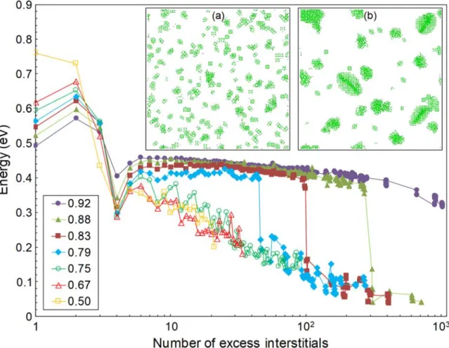
In Fig. 1 we plot the mean energy of DAs within I-clusters generated during the annealing simulations as a function of their size. For the three lowest temperatures, cluster energies decrease
with size showing local minima at some “magic” numbers corresponding to very stable
configurations, in agreement with results from other authors [4,12,17]. In our MD simulations,
many Is are aggregated in the form of the Arai tetra-I, in agreement with first-principle calculations that predict such configuration as the lowest formation energy I-cluster in Si [28,29]. There are also a few small agglomerates of tetra-Is with 8, 12, 16 Is and so on [11], which precisely coincide with the local minima observed in Fig. 1. Some <011> chains are also generated,
which are considered the precursors of {113} defects [18], as well as several {111} rod-like defects
(see Fig. 1(a) in Ref. [30]). Our results indicate that, for the lowest simulated temperatures, I aggregation is consistent with a conventional OR process with dominance of stable ordered
structures (Tersoff 3 potential is consequently able to correctly predict the OR driven I-cluster growth observed at conventional annealing conditions). However, for temperatures T* of 0.79 and
plateaus with a quasi-continuous energy distribution followed by sharp energy drops. In our MD
simulations the Arai tetra-I is the only ordered atomic structure present at such high temperatures, due to its high vibrational entropy, as it was calculated by Kapur and Sinno [17]. Energy plateaus
are indicative of the presence of disordered I-clusters, whose dominance at high temperatures is favored with respect to ordered structures due to their high configurational entropy [31]. The
existence of these high entropy amorphous configurations of Is at high temperatures is in line with the “morph” postulated by Cowern and coworkers to explain high-temperature diffusion
experiments in Si and Ge [32]. Even though disordered I-clusters in our simulations may involve tens of excess Is and even hundreds of DAs, we observe that they are highly mobile and rapidly grow by interacting with other mobile disordered aggregates or immobile tetra-Is. When they reach a certain size, they spontaneously transform into ordered planar EDs where I atoms are concentrated in a disk perpendicular to the <001> direction, and consequently they can be
described as {001} loops (see Fig. 1(b) in Ref. [30]). This structural transformation corresponds
to the sharp drops in the energy curves of Fig. 1. It is worth noting that higher temperatures produce
fewer but larger {001} loops, in agreement with experiments [20]. However, at the highest
simulated temperature T* = 0.92 no loops are observed, just one large disordered cluster that
encompasses all the Is formerly introduced in the lattice (see Fig. 2 in Ref. [30]).
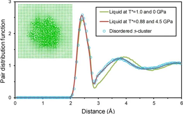
We have investigated the inner structure of these I-aggregates through the calculation of the pair distribution function (PDF). As an example, Fig. 2 illustrates the PDF of a large disordered I-cluster formed during annealing at T* = 0.88. The graph also shows the PDF of two liquids in
equilibrium (both simulated with periodic boundary conditions), one at the melting temperature
with zero external pressure, and the other one at T* = 0.88 under 4.5 GPa of compressive stress.
indicates that the high local stress generated to accommodate the excess I-atoms into the solid medium actually transforms them into high-density liquid droplets. Extra density with respect to a
zero pressure liquid is evidenced by a higher first neighbor peak and a closer second-neighbor
shell. Another evidence of the liquid nature of the I-aggregates is that the integral up to the first minimum of the corresponding PDF gives a value close to 6, typical of metallic liquid Si, unlike
the value of 4 of semiconducting amorphous Si. The liquid nature of these I-clusters explains the high mobility they show in our simulations (see Fig. 3 in Ref. [30]).
The liquid droplets adopt a quasi-spherical shape to minimize the surface-to-volume ratio
and consequently the defect interfacial energy. We have observed that when two liquid I-aggregates diffusing through the Si lattice interact, first a “neck” connecting both pockets is
generated, and then fast atomic redistribution leads to the recovery of the spherical shape in the
final droplet (see Fig. 4 in Ref. [30]). This kind of process, known as coalescence, is common for
defect coarsening in metals [33-35]. However, our work appears to be the first evidence of such a
mechanism for ED growth in solid semiconductors. It is interesting to note that, when coalescence
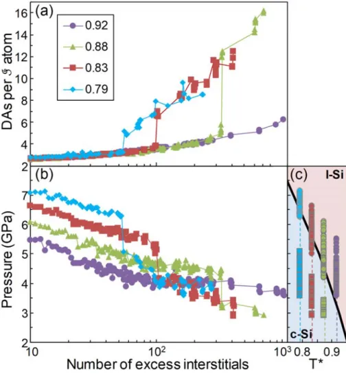
is completed and a new larger sphere is formed, the total number of excess Is equals the sum of Is in the merging clusters, but the final number of DAs in the resulting defect is larger than the sum of initial DAs. Figure 3(a) shows the ratio of DAs per I atom in every I-cluster generated during the annealing simulations at high temperatures. The rise in the number of DAs per I with cluster size contributes to release the misfit strain energy due to a better accommodation of excess
Is within the clusters, which compensates for the increase of volume and interfacial energies due to a larger number of DAs. As a consequence, with increasing number of excess Is, liquid I-aggregates tend to occupy a larger volume per I atom within the lattice, which leads to a hydrostatic pressure release within the I-rich droplets as shown in Fig. 3(b).
Liquid I-clusters grow until they spontaneously precipitate into immobile planar {001} loops. After the structural transformation, the ratio of DAs per I atom significantly increases with size, as it can be seen in Fig. 3(a), indicating that in {001} loops extra I atoms produce strong strain fields that distort the surrounding lattice much more than when they belong to liquid I-clusters. This allows a further release of hydrostatic pressure within the defect, as shown in Fig
3(b). The structural transformation occurs at cluster sizes that increase with annealing temperature,
which explains why higher temperatures produce fewer but larger {001} loops. In turn, the defect
pressures at which the structural transformation is triggered decrease with annealing temperature.
In Fig. 3(c) we have plotted these hydrostatic pressure values as a function of reduced temperatures
along with the solid-liquid equilibrium line in the Si phase diagram (from Ref. [36]). At the early
stages of the annealing simulations, generated I-clusters are small and the corresponding points in the diagram are above the solid-liquid equilibrium line. As these liquid I-clusters coalesce and grow, their associated hydrostatic pressure decreases until they cross the solid-liquid equilibrium
line. Then liquid I-droplets become undercooled, and after some incubation period they transform into regular {001} loops. The clear correlation between the temperature and pressure values for
the transformation of liquid I-droplets into {001} loops with the solid-liquid equilibrium line in the Si phase diagram indicates that such transformation is in fact a first order liquid-to-solid
transition. As stated earlier, no structural transformation is observed in our simulation at T* = 0.92.
From the phase diagram of Si, at this temperature the pressure within the liquid I-clusters should drop close to 3.3 GPa for the structural transformation to occur, and that would require a cluster
size larger than the total number of Is considered in this work.
Our simulations have revealed that the structural transformation into {001} loops starts with
in Ref. [30]). This high vibrational entropy defect can withstand temperatures close to the Si
melting point [17]. In addition, its atomic structure, where all atoms are perfectly four-fold
coordinated, favors their formation at the interface between the liquid aggregates and the crystal
lattice, naturally accommodating the excess I content (extra density) of the high-pressure liquid droplets. Once nucleated, Arai tetra-Is act as a template that promote the fast liquid droplet crystallization.
Our MD results suggest a purely kinetic explanation for the formation of {001} loops, where
the liquid-to-solid transition, as well as the final defect size, only depends on local temperature.
The defect formation mechanism should be, in principle, independent from the thermal stress
developed during the annealing process (unlike it was suggested in Ref. [20]). In order to further
support these findings we have performed dedicated LA experiments in which Si on insulator
(SOI) substrates were used in order to modify the thermal biaxial strain with respect to
conventional Si bulk substrates, and bring it below the theoretical level for the inversion of stability
between {111} and {001} loops.
A 320 nm-thick SOI wafer (BOX = 1 m) and a reference Czochralski (001) Si wafer were implanted with 80 keV Si+ to a nominal dose of 2×10¹⁴ ions/cm2. These conditions ensure the
formation of large I-rich regions, while keeping the damage below the amorphization threshold. Several square areas (10×10 mm2) of the implanted wafers were laser annealed using a
SCREEN-LASSE LT system based on pulsed UV irradiation (λ = 308 nm, pulse duration < 200 ns), with
laser energy densities ranging from 0.6 to 1.1 J/cm2 for the SOI wafer and 1.5 to 2.9 J/cm2 for the
reference Si sample. A single laser pulse was used in all cases. These conditions were chosen on
different substrates. TEM analysis, using weak-beam dark-field imaging conditions, was
performed to investigate the position and nature of defects formed during LA.
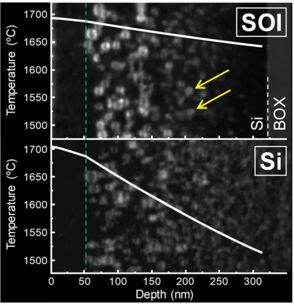
In Fig. 4 we show two cross-section TEM micrographs from the SOI substrate annealed at
0.9 J/cm2 and from the reference Si sample annealed at 2.3 J/cm2, as well as the corresponding
local maximum temperature profiles calculated by means of phase-field simulations. These
simulations foresee a ~ 55 nm melt depth for the two cases, which is confirmed by the thicknesses
of the surface regions denuded from defects as seen in the TEM analysis.
The thermo-elastic evaluation of the upper limit of the stress field in the two cases (see Fig.
6 in Ref. [30]) is strongly different: ~ -1 GPa for the bulk Si and ~ -0.2 GPa for the SOI case. This
is mainly due to the particular temperature distribution in the SOI system, where the maximum
temperature gradient is obtained in the oxide layer (the estimated maximum temperature drops
from ~ 1640 K to ~ 410 K in the 1 m-thick oxide layer). The low stress field estimated in the SOI case results in a very small increase of the formation energy of {111} loops (see Fig. 7 in Ref.
[30]), in such a way that the inversion of the stability from {111} to {001} defects, predicted in
the reference Si case, is not expected in SOI. However, in spite of the unfavorable energetic
argument, and similarly to the Si reference case, the dislocation loops observed in the LA
processed SOI sample (top of Fig. 4) are still of {001} type, as confirmed by the gb contrast method [38] performed on this sample (see Fig. 8 in Ref. [30]). Moreover, their size distribution
is less dependent with depth compared to the reference Si case. While {001} loops exhibiting a
diameter of ~ 5 nm are clearly visible in the SOI sample at a depth of ~ 200 nm (yellow arrows in
Fig. 4), they have a much smaller size in the Si sample at the same depth, in agreement with the
comparing the SOI sample annealed at 1.1 J/cm2 with the Si reference sample annealed at
2.6 J/cm2, for which the expected melt depth was ~ 110 nm (see Figs. 6 and 9 in Ref. [30]). Results
lead to the same conclusions in terms of defect nature, location and relation to the stress impact on
the defect formation energy, in good agreement with the MD simulation predictions presented in
this work.
In summary, we have shown using MD techniques that {001} loops form as the result of a
local liquid-solid transition in I-rich droplets embedded in the Si crystal which generate at temperatures close to the melting point. The high mobility of such liquid I-aggregates and their fast growth by coalescence explains how the transition to {001} loops occurs in ultrafast
(nanoseconds wide) time scales, with respect to the typical time scales (seconds) for the formation
of EDs in Si via the conventional OR mechanism. These results are in perfect agreement with the
experimental evidence of instantaneous formation of {001} loops in nanosecond laser annealed
Si, even in the absence of thermal-induced stress.
ACKNOWLEDGEMENTS
This work has been supported by the EU (FEDER) and the spanish Ministerio de Economía
y Competitividad under Project No. TEC2014-60694-P, and by the Junta de Castilla y León under
Project No. VA331U14. F.C. and A.L. acknowledge the cooperation project between CNR and
Figure 1. Dependence of the I-cluster mean energy per DA with size at several annealing
temperatures. Energies are measured with respect to the perfect crystal. At each temperature,
energy values have been obtained by averaging the energy per DA for all I-clusters with the same size, no matter their particular atomic configuration. The different I-cluster morphologies at low and high temperatures are illustrated in the snapshots, corresponding to ZY projections of DAs
within the simulation cell taken after 10 ns annealing at (a) T* = 0.50, showing tetra-Is, small <011> chains and {111} rod-like defects; and (b) T* = 0.79, showing tetra-Is, large disordered I-clusters and {001} loops.
Figure 2. Inset: ZY view of a disordered I-cluster formed during annealing at T* = 0.88. Main
Figure 3. Dependence with I-cluster size of (a) the ratio of DAs per I atom, and (b) the cluster
hydrostatic pressure. Values have been obtained by averaging for all I-clusters with the same size at each temperature. In (c) pressure values are represented as a function of T* along with the
solid-liquid equilibrium line of the Si phase diagram. Circles correspond to solid-liquid I-clusters and squares to {001} loops.
Figure 4. Cross-section TEM micrographs from the SOI substrate annealed at 0.9 J/cm2, and the
bulk Si substrate annealed at 2.3 J/cm2. Superimposed are the corresponding local maximum
temperature profiles calculated by phase-field simulations. Green dashed line indicates the melt
REFERENCES
[1] M. Ieong, B. Doris, J. Kedzierski, K. Rim, and M. Yang, Science 306, 2057 (2004).
[2] D. J. Eaglesham, P. A. Stolk, H. J. Gossmann, and J. M. Poate, Appl. Phys. Lett. 65, 2305
(1994).
[3] J. Li and K. S. Jones, Appl. Phys. Lett. 73, 3748 (1998).
[4] N. E. B. Cowern, G. Mannino, P. A. Stolk, F. Roozeboom, H. G. A. Huizing, J. G. M. van
Berkum, F. Cristiano, A. Claverie, and M. Jaraíz, Phys. Rev. Lett. 82, 4460 (1999).
[5] S. Coffa, S. Libertino, and C. Spinella, Appl. Phys. Lett. 76, 321 (2000).
[6] S. Libertino, S. Coffa, and J. L. Benton, Phys. Rev. B 63, 195206 (2001).
[7] A. Claverie, B. Colombeau, B. de Mauduit, C. Bonafos, X. Hebras, G. Ben Assayag, and F.
Cristiano, Appl. Phys. A 76, 1025 (2003).
[8] A. Claverie, B. Colombeau, F. Cristiano, A. Altibelli, and C. Bonafos, Nucl. Instrum.
Methods Phys. Res., Sect. B 186, 281 (2002).
[9] I. Avci, M. E. Law, E. Kuryliw, A. F. Saavedra, and K. S. Jones., J. Appl. Phys. 95, 2452
(2004).
[10] N. Zographos, C. Zechner, and I. Avci, Mater. Res. Soc. Symp. Proc. 994, 0994-F10-01
(2007).
[11] S. Lee and G. S. Hwang, Phys. Rev. B 77, 085210 (2008).
[12] S. Lee and G. S. Hwang, Phys. Rev. B 78, 045204 (2008).
[13] S. S. Kapur and T. Sinno, Phys. Rev. B 82, 045205 (2010).
[14] S. S. Kapur, A. M. Nieves, and T. Sinno, Phys. Rev. B 82, 045206 (2010).
[15] S. K. Estreicher, M. Gharaibeh, P. A. Fedders, and P. Ordejón, Phys. Rev. Lett. 86, 1247
[16] I. Martin-Bragado, M. Jaraiz, P. Castrillo, R. Pinacho, J. Barbolla, and M. M. De Souza, Phys.
Rev. B 68, 195204 (2003).
[17] S. S. Kapur and T. Sinno, Appl. Phys. Lett. 93, 221911 (2008).
[18] S. Takeda, Microsc. Res. Techniq. 40, 313 (1998).
[19] F. Cristiano, J. Grisolia, B. Colombeau, M. Omri, B. de Mauduit, A. Claverie, L. F. Giles,
and N. E. B. Cowern, J. Appl. Phys. 87, 8420 (2000).
[20] Y. Qiu, F. Cristiano, K. Huet, F. Mazzamuto, G. Fisicaro, A. La Magna, M. Quillec, N.
Cherkashin, H. Wang, S. Duguay, and D. C. Blavette, Nano Lett. 14, 1769 (2014).
[21] J. Tersoff, Phys. Rev. B 38, 9902 (1988).
[22] S. Munetoh, K. Moriguchi, K. Kamei, A. Shintani, and T. Motooka, Phys. Rev. Lett. 86, 4879
(2001).
[23] L. A. Marqués, L. Pelaz, M. Aboy, L. Enríquez, and J. Barbolla, Phys. Rev. Lett. 91, 135504
(2003).
[24] K. J. Dudeck, L. A. Marqués, A. P. Knights, R. M. Gwilliam, and G. A. Botton, Phys. Rev.
Lett. 110, 166102 (2013).
[25] L. A. Marqués, L. Pelaz, J. Hernández, J. Barbolla, and G. H. Gilmer, Phys. Rev. B 64, 045214
(2001).
[26] S. Plimpton, J. Comput. Phys. 117, 1 (1995).
[27] L. A. Marqués, L. Pelaz, P. Castrillo, and J. Barbolla, Phys. Rev. B 71, 085204 (2005).
[28] N. Arai, S. Takeda, and M. Kohyama, Phys. Rev. Lett. 78, 4265 (1997).
[29] B. J. Coomer, J. P. Goss, R. Jones, S. Öberg, and P. R. Briddon, J. Phys. Condens. Matter 13,
L1-L7 (2001).
[31] C. Y. Chuang, A. Sattler, and T. Sinno, J. Appl. Phys. 117, 135706 (2015).
[32] N. E. B. Cowern, S. Simdyankin, C. Ahn, N. S. Bennett, J. P. Goss, J.-M. Hartmann, A.
Pakfar, S. Hamm, J. Valentin, E. Napolitani, D. De Salvador, E. Bruno, and S. Mirabella,
Phys. Rev. Lett. 110, 155501 (2013).
[33] R. S. Barnes and D. J. Mazey, Proc. R. Soc. A 275, 47 (1963).
[34] A. Weck, D. S. Wilkinson, E. Maire, and H. Toda, Acta Mater. 56, 2919 (2008).
[35] T. D. Swinburne, K. Arakawa, H. Mori, H. Yasuda, M. Isshiki, K. Mimura, M. Uchikoshi,
and S. L. Dudarev, Sci. Rep. 6, 30596 (2016).
[36] C. C. Yang, J. C. Li, and Q. Jiang, Solid State Commun. 129, 437 (2004).
[37] K. Huet, G. Fisicaro, K. Venturini, H. Besaucele, and A. La Magna, Appl. Phys. Lett. 95,
231901 (2009).
[38] D. B. Williams and C. B. Carter, Transmission Electron Microscopy. A Textbook for