Carbon Nanotube-Based Nanorelays for
Low-Power Circuit Applications
by MASSACHUS OF TEC Courtney E. Schmitt
AUG
B. S., Electrical Engineering,The Pennsylvania State University, May 2007
LIBR
ETTS INSTfTUTE
CHNOLOGY
07 2009
ARIES
Submitted to the Department of Electrical Engineering and Computer Science in Partial Fulfillment of the Requirements for the Degree of
Master of Science in Electrical Engineering and Computer Science at the
Massachusetts Institute of Technology June 2009
© 2009 Massachusetts Institute of Technology All rights reserved
Signature of Author ... ...
Department of Electrical Engineering and
ARCHIVES
Computer Science June 5, 2009 Certified by ... ... ... ...
Anantha P. Chandrakasan Joseph F. and Nancy P. Keithley Professor of Electrical Engineering Thesis Supervisor Accepted by ... ...
'/ Professor Terry P. Orlando Chair, Department Committee on Graduate Students Department of Electrical Engineering and Computer Science
Carbon Nanotube-Based Nanorelays for
Low-Power Circuit Applications
by
Courtney E. Schmitt
Submitted to the Department of Electrical Engineering and Computer Science On May 8, 2009 in Partial Fulfillment of the
Requirements for the Degree of Master of Science in Electrical Engineering and Computer Science
Abstract
The objective of this research is to reduce static power dissipation by developing a vertically-oriented carbon nanotube-based nanoelectromechanical switch that has no off-state leakage current. This switch, called a nanorelay, is a mechanical switch that uses a carbon nanotube as the active component. The device consists of a line of carbon nanotubes grown on a highly-doped silicon substrate between two contacts that are electrically isolated from the substrate by an insulator.
The nanorelay is actuated when a control voltage is applied between the substrate and either one of the contacts. This voltage causes the nanotube to be pulled into and eventually make physical contact with one of the contacts, which allows current to flow through the carbon nanotube. During the off state, a physical gap separates the nanotube from the contact which acts as a near-ideal tunneling barrier to virtually eliminate leakage currents. Since the nanorelay has almost no static power dissipation, it has many potential applications in low-power circuit design.
This thesis makes three main contributions. First, a fabrication process to construct nanorelays is presented. Second, potential low-power circuit applications of the nanorelay are explored and implemented in a CMOS test chip. Finally, a test system is developed in order to characterize and quantify the static power savings benefits of using the nanorelay for low-power circuit applications.
Thesis Supervisor: Anantha P. Chandrakasan
Acknowledgements
This thesis would not have been possible without the help and guidance I received from many people during my first two years at MIT.
First, I would like to thank Professor Anantha Chandrakasan for providing me with direction, circuit advice, and most importantly the opportunity to do this research. I would also like to thank Professor Tayo Akinwande and Dr. Luis Velasquez-Garcia for their input on the fabrication process, and Professor Marc Baldo for his guidance and advice.
I am extremely grateful for the collaboration of Kaveh Milaninia, who is a genius process
engineer and material scientist. Kaveh spent many hours in the fab showing me how to create devices and teaching me everything I know about fabrication processes. Thanks also to all the members of Ananthagroup for answering my tapeout questions and helping me with circuit design issues.
Thank you to my family for their continued support through the many years of my education, and to the friends I have made at MIT for making my time here more enjoyable.
Finally, I would like to acknowledge FCRP IFC and DARPA for funding this project, National Semiconductor for the test chip fabrication, and the Microsystems Technology Laboratories (MTL) and NanoStructures Laboratory (NSL) at MIT for providing the tools for device fabrication.
Table of Contents
A b stract ... ... ... ... ... ... ... 3
A cknow ledgem ents ... ... ... 4
T able of C ontents ... ... 6
L ist of F igu res ... .. ... ... ... ... 8
1 Introduction ... 11
1.1 Background and Motivation ... 11
1.2 Carbon Nanotube-Based Nanorelays ... 11
1.3 Previous Work ... 13
1.4 Thesis C ontributions ... .... 18
2 Nanorelay Device Structure and Fabrication Process... 19
2.1 Device Design ... 20
2.1.1 Device Structure... ... 20
2.1.2 Device Dimensions ... ... 21
2.2 Carbon Nanotube Synthesis ... 24
2.2.1 Growth Temperature ... 24
2.2.2 G row th Tim e ... 26
2.2.3 Catalyst Material ... ... 27
2.2.4 Catalyst Thickness ... ... 29
2.3 Device Fabrication ... ... 31
2.3.1 Formation of a Line of Vertically Aligned CNTs... 33
2.3.2 Formation of the Gap and Contact Terminals... 36
2.3.3 Release of the CNTs ... ... 40
3 Nanorelay Device Characterization ... ... 49
3.1 Experimental Setup ... 49
3.2 Pull-in Voltage ... .. ... 49
3.3 On-Resistance ... 51
4 Low-Power Circuit Applications and CMOS Test Chip... 53
4.1 Circuit Applications ... 53
4 .1.1 P ow er G atin g ... 53
4.1.2 N onvolatile SR A M ... ... 60
4.1.3 Reconfigurable Interconnect ... ... 63
4.1.4 Digital Logic ... .. ... 64
4.2 CMOS Test Chip... .... . ... 65
5 Nanorelay-CMOS Test System Implementation and Results... 67
5.1 Test Setup... .. . ... 67
5.2 PCB Design... ... ... 69
5.3 N anorelay Packaging ... 70
5.4 Test System R esults ... ... 71
5.4.1 Power Gating ... ... 72
5.4.3 Reconfigurable Interconnect ... ... 75
6 Conclusions and Future Work ... 76
6.1 Thesis Summary and Main Contributions ... 76
6.2 Suggestions for Future W ork ... 76
6.2.1 Nanorelay Device Optimization ... 77
6.2.2 System Demonstration ... ... ... 77
6.2.3 Control Terminal Isolation... ... 78
List of Figures
Figure 1-1. Figure Figure Figure 1-2. 1-3. 1-4. Figure 1-5. Figure 1-6. Figure 1-7. Figure Figure Figure Figure Figure 1-8. 1-9. 2-1. 2-2. 2-3. Figure 2-4. Figure 2-5. Figure 2-6. Figure 2-7 Figure 2-8 Figure 2-9 Figure 2-1 Figure 2-1 Figure 2-1(a) Device schematic of a vertically oriented nanorelay. (b) Nanorelay upon actuation using an applied voltage between the substrate and a
contact ... . . ... 12
Basic operation of the nanorelay ... ... 13
CNT-based cantilever switch [8]. ... 14
I-VsG data for a CNT-based cantilever device. The first current jump indicates the voltage where the CNT pulls into the drain contact; the second jump indicates the voltage where the CNT pulls into the gate contact [8] ... ... 14
Schematics of the vertical, multi-CNT switch, (a) the three tube version, (b) the two tube version, (c) the three tube version under activation, and (d) the two tube version under activation [9]. ... .. ... 15
(a) Left: SEM micrograph of the fabricated three tube CNT switch. Right: SEM micrograph of the same device after the removal of an applied bias. The scale bar corresponds to 1 pm. (b) I-VsG data for the three tube CNT sw itch [9]... ... ... .. ... ... ... ... 16
a) Left: SEM micrograph of the fabricated two tube CNT switch. Right: SEM micrograph of the same device after removal of an applied bias. The scale bar corresponds to 1 pm. (b) I-VsG data for the two tube CNT switch [9] ... .. . . .. . . .. ... . ... 16
Schematic of vertical CNT-based switch [10]. ... 17
A fabricated vertical CNT-based switch with misaligned contacts [10]... 17
SEM of self-aligned carbon nanotube-based micro ionizer [16], [17] ... 19
3-dimensional model of the nanorelay device. ... 21
(a) Electrostatic, elastostatic, and van der Waals forces acting on the CNT during pull-in. (b) Nanorelay device dimensions. ... 23
CNT growth: 6750 C for 30 minutes with a 10 nm nickel catalyst ... 25
CNT growth: 8250 C for 30 minutes with a 10 nm nickel catalyst ... 25
CNT growth: 8250 C for 15 minutes with a 30 nm nickel catalyst ... 26
CNT growth: 8250 C for 30 minutes with a 30 nm nickel catalyst ... 27
CNT growth: 8250 C for 30 minutes with a 10 nm nickel catalyst ... 28
CNT growth: 8250 C for 30 minutes with a 10 nm iron catalyst. ... 28
0. CNT growth: 825" C for 30 minutes with a 10 nm cobalt catalyst ... 29
1. CNT growth: 8250 C for 30 minutes with a 10 nm nickel catalyst ... 30
Figure Figure Figure Figure Figure Figure Figure Figure Figure Figure Figure Figure Figure Figure Figure Figure Figure Figure Figure Figure Figure
2-13. Nanorelay fabrication process steps... 32
2-14. Electron beam lithographically patterned Ni catalyst dots, M=3.5K X... 34
2-15. Electron beam lithographically patterned Ni catalyst dots, M=84K X... 34
2-16. Line of carbon nanotubes, tilt=0 . ...... . . .... . . . . .. .. 35
2-17. Line of carbon nanotubes, tilt=30.... ... ... .. ... . . . . 36
2-18. Line of nanotubes covered with conformal SiO2 and a-Si, tilt=300 . ....... 38
2-19. a-Si bonding and probe pads leading to CNT line, tilt=30....... ... . . ... .. 38
2-20. Patterned photo resist, tilt=30 . ...... . . . . .. . . 39
2-21. Etch of exposed a-Si on tips of nanotubes, tilt=0. ... . . . ..... . . 39
2-22. a-Si contact after resist has been stripped, tilt=30 . ... 40
2-23. Forest of CNTs showing effects of stiction forces after wet etch, tilt=30°. 4 2 2-24. Effects of stiction forces on line of CNTs, tilt=0.... ... . ... . . 42
2-25. Completed device after BOE release, tilt=30. ... . . ...... 43
2-26. Completed device after BOE release, tilt=0 . ...... . . ... .43
2-27. Line of CNTs after vapor HF release, tilt=00.... ... ... ... . . . ...... . . . . 44
2-28. Line of CNTs after vapor HF release, tilt=0... . . . ...... . . . . 45
2-29. Completed device after vapor HF release, tilt=30 . .... ... ... . . . ...... 45
2-30. Forest of CNTs showing no stiction effects after critical point dry, tilt= 30 . . . . ..... ... ... . . . . 47
2-31. Line of CNTs after critical point dry release, tilt=300. ...... .. .... . ...... 47
2-32. Completed device after critical point dry release, tilt=300....... ... . ... . 48
3-1. Measured I-V data for a fabricated nanorelay device. Run 1 shows the pull-in voltage of 12.5 V, Run 2 shows that the CNT stayed on the contact after the control voltage was removed ... ... 51
3-2. Measured I-V data for fabricated nanorelay devices in the on-state showing an average contact resistance of 600 MQ. ... 52
4-1. Nanorelay used as a power footer during (a) active mode, and (b) idle m ode ... ... . . . 54
4-2. Simulation of power gating with idle time < break even time ... 56
4-3. Simulation of power gating with idle time > break even time ... 56
4-4. Schematic diagram of circuit used for break even time simulation ... 58
4-5. Break even time energy domain simulation results. ... 59
4-6. Break even time power domain simulation results ... 59
4-7. Simulated response of FIR to a single bit pulsed input... 60 Figure Figure Figure Figure Figure Figure Figure Figure
Figure 4-8. (a) Nonvolatile memory cell with a nanorelay storage device and CMOS pass gates. (b) Nonvolatile memory cell constructed entirely from
nanorelays ... .. ... 61
Figure 4-9. Basic operation of the nanorelay SRAM cell. (a) Write operation: write wordline is high, connecting bitlines to the control terminals, which sets the state of the nanorelay. (b) Read operation: read wordline is high, connecting the bitlines to the signal terminals. The terminal connected to the nanorelay is pulled low, which results in a voltage drop on the bitline... 61
Figure 4-10. Operation of nanorelay SRAM cell simulated using HSPICE... 62
Figure 4-11. Frequency-programmable ring oscillator using nanorelays for reconfigurable interconnect. ... 63
Figure 4-12. Oscillation of the long and short inverter paths in the ring oscillator as simulated in Nanosim. ... . ... 64
Figure 4-13. Digital logic gates constructed from nanorelays ... 65
Figure 4-14. Layout and die photo of the nanorelay test chip. ... 66
Figure 5-1. Schematic diagram of nanorelay-CMOS test system setup ... 68
Figure 5-2. Experimental nanorelay-CMOS test system setup ... 69
Figure 5-3. Printed circuit board (PCB) for nanorelay-CMOS test system ... 70
Figure 5-4. Packaged nanorelay device. ... 71
Figure 5-5. Measured response of FIR to a single bit pulsed input ... 72
Figure 5-6. M easured operation of SRAM cell. ... ... 74
Figure 5-7. Measured response of the frequency-programmable ring oscillator output as the inverter path is switched from long to short ... 75
Figure 6-1. Programming operation for three- and five-terminal nanorelays ... 78
Chapter 1
1 Introduction
1.1 Background and Motivation
Static power dissipation has recently become one of the most pressing concerns in CMOS circuit design. As CMOS transistors continue to scale to smaller dimensions, leakage current becomes a more significant portion of the overall circuit power consumption
[1]. Excessive power consumption leads to many other issues including decreased
battery life, decreased reliability, and increased cooling costs. A significant portion of static power dissipation occurs when the circuit is idle because of undesired leakage currents through the transistors. Consequently, there has been much interest in minimizing off-state leakage currents to reduce the energy used in CMOS circuits.
The first major source of leakage current in CMOS transistors is subthreshold leakage, where current flows through the channel in the off state. The subthreshold leakage is exponentially related to the supply voltage applied to the gate. For newer technologies, this supply voltage has been decreased to reduce the dynamic power consumption and improve reliability. As a result, the subthreshold current has also increased with transistor scaling. The second major leakage source is gate leakage, which occurs when electrons tunnel through the gate oxide. Since a thin oxide layer is desirable for performance, the thickness of the oxide separating the gate has been decreased with each new technology node. As the oxide becomes thinner, it is easier for electrons to tunnel
though, increasing the gate leakage current [1].
1.2 Carbon Nanotube-Based Nanorelays
In CMOS transistors, there is a tradeoff between performance and power consumption. In order to control static power dissipation without decreasing the CMOS performance, this thesis proposes a new device that eliminates leakage currents: the carbon nanotube-based nanorelay. A nanorelay is a vertical nanoelectromechanical
system (NEMS) switch that uses a multi-wall carbon nanotube [2], [3] as the actuating device. Unlike silicon CMOS, nanorelays use a physical gap to isolate the terminals during the off state. During the off state, the size of the physical gap increases and the CNT moves away from the contact. As a result, nanorelays have the potential to nearly eliminate static leakage power dissipation [4]. Carbon nanotubes are used as the actuators because they have excellent current-carrying capabilities, are flexible and durable, have high aspect ratios, and can withstand much higher temperatures than silicon devices [5]. Consequently, nanorelays have the potential to operate at higher clock
frequencies, and they open up the possibility for new high temperature applications.
The nanorelay is a NEMS switch that uses a vertically-grown carbon nanotube (CNT) as the active component. Figure 1-1 (a) shows the device schematic. The nanorelay consists of a line of CNTs grown directly on a highly doped silicon substrate between two contacts that are electrically isolated from the substrate by an insulator. The nanorelay is actuated when a voltage is applied between the substrate and one of the contacts. This voltage attracts the CNT, pulling it in towards the contact [6]. The CNT eventually connects with the contact, allowing current to flow through the CNT to the substrate, as shown in Figure 1-1 (b).
Carbon
Nanofiber
Contact
Insulator
(a) (b)
Figure 1-1. (a) Device schematic of a vertically oriented nanorelay. (b) Nanorelay upon actuation using an applied voltage between the substrate and a contact.
Once the nanorelay has been programmed, the nanorelay will hold its state even after the applied voltage is removed because of the adhesive van der Waals forces between the CNT and the contact [7]. In order to switch the nanorelay again, a voltage must be applied to the opposite terminal to overcome the van der Waals force and pull the CNT off of the original contact and in to the desired contact. This operation is illustrated in Figure 1-2, where the nanorelay is electrically modeled as a single-pole double-throw switch.
initial switch left hold switch right hold
Figure 1-2. Basic operation of the nanorelay.
1.3 Previous Work
The first CNT-based switch was developed by Lee et al at G6teborg University and Chalmers University of Technology in 2004 [8]. This paper describes the fabrication of a three terminal switch and proposes several potential applications for the field, including logic, memory, amplifiers, mechanical tweezers, sensors, and resonators. The device proposed in this paper uses a CNT as the cantilever in a conventional cantilever beam resonator, as shown in Figure 1-3. In this switch, a control voltage is applied to the gate
G, which causes the CNT to deflect and eventually make contact to the drain D. Once
7a ~ -- z
Figure 1-3. CNT-based cantilever switch [8].
There are several issues with this device. First, the switch relies solely upon the elastic force of the CNT to disconnect the source from the drain when the gate voltage is removed. This elastic force is often not strong enough to restore the CNT to its original position, causing the CNT to act as a permanent short circuit between the source and drain electrodes. A second problem with this device is that the CNT can unintentionally make contact with the gate electrode, leading to a short circuit between the source and gate. This is illustrated in the I-VsG curve in Figure 1-4; initially the CNT is disconnected, then at 5 V the CNT is pulled into the drain, and then finally at 6 V it is pulled into the gate.
100- 80-. 0 60-40 2 0-VSD=5 I I Mecluical Con
/
Votage CV) 00mtV tact -- --- I 0 1 2 3 4 5 6 VGate (V)Figure 1-4. I-VsG data for a CNT-based cantilever device. The first indicates the voltage where the CNT pulls into the drain contact; the indicates the voltage where the CNT pulls into the gate contact [8].
current jump second jump
A second CNT-based NEMS switch design was proposed by Jang et al at the University of Cambridge in 2005 [9]. This design used several vertically-oriented CNTs grown in predefined locations on top of the contact electrodes, as shown in Figure 1-5. The CNTs are individually charged to specific voltages so that the drain and source tubes are attracted to each other. This attraction causes the tubes to deflect towards each other, eventually making contact to allow current flow.
(a) (b)
-+ -+
-+ -+
(c) (d)
Figure 1-5. Schematics of the vertical, multi-CNT switch, (a) the three tube version, (b) the two tube version, (c) the three tube version under activation, and (d) the two tube version under activation [9].
This design is an improvement over the cantilever structure because the gate electrode can be used to pull the central drain CNT away from the source CNT to stop current flow. However, it is still possible for the drain CNT to undesirably short to the gate CNT, as in the cantilever structure. Another issue with this vertical CNT design is stiction between the drain and source CNTs. Since both CNTs deflect, there will be strong van der Waals stiction forces between the tubes, making it difficult to disconnect the drain from the
source. The pull-in voltage of this device is fairly high since the CNTs do not have a high aspect ratio, and the current carrying capability is low because of poor contacts between the CNTs and the electrodes, but pull-in was observed both optically and electrically, as shown in Figure 1-6, clearly demonstrating the proof-of-concept design.
0 107 4-0 - V21nd=0.O5V 10 0 0 21 22 23 Voltage-3rd CNT(V) (a) (b)
Figure 1-6. (a) Left: SEM micrograph of the fabricated three tube CNT switch. Right: SEM micrograph of the same device after the removal of an applied bias. The scale bar corresponds to 1 pm. (b) I-VsG data for the three tube CNT switch [9].
-* 2nd A 3rd 10a 2 V2nd=0.05V 10" 0 00 22 24 26 Voltage(V) (a) (b)
Figure 1-7. a) Left: SEM micrograph of the fabricated two tube CNT switch. Right: SEM micrograph of the same device after removal of an applied bias. The scale bar corresponds to 1 pm. (b) I-VsG data for the two tube CNT switch [9].
The next advance in CNT-based NEMS switches was made by Kaul et al at NASA JPL in 2006 [10]. This design also utilized a vertical-CNT approach, but moved the metal contact electrodes to be in-line with the top of the CNT, as shown in Figure 1-8. This has the advantage of placing the stable, stationary contact points in close proximity with the flexible end of the CNT. The disadvantage of this design is that the alignment of the
metal electrodes to the CNT is not very well controlled. A fabricated device with misaligned contacts is shown in Figure 1-9.
CNT..
Figure 1-8. Schematic of vertical CNT-based switch [10].
Figure 1-9. A fabricated vertical CNT-based switch with misaligned contacts [10]. The nanorelay proposed in this thesis improves upon this final design in two ways. First, a self-align process is used to pattern the metal contacts around the CNT, eliminating misalignment errors. Second, the distance between the CNT and the contacts is reduced to minimize the pull-in voltage of the switch.
Another relevant area of research is exploring potential applications for NEMS devices. NEMS switches find many applications in the area of low-power circuit design because they have no off-state leakage currents. Chen et al at MIT and the University of California at Berkeley have considered several NEMS switch circuit applications, including digital logic, I/O switches, digital-to-analog converters, and flash analog-to-digital converters [11]. The Verilog-A simulation results from this work showed that using NEMS switch circuits can be up to ten times more efficient than tradition CMOS circuits. The tradeoff for this power savings is a larger delay time introduced by the mechanical switching of the NEMS device.
Similarly, Chakraborty et al at Case Western University have investigated potential applications for carbon nanotube-based NEMS switches [12]. These applications include reducing leakage in digital logic and memory circuits. HSPICE simulation results show that these circuit applications take advantage of the low-leakage properties of NEMS switches and the excellent electrical properties of carbon nanotubes.
In addition to NEMS devices, there has been a large amount of interest in fabricating a carbon nanotube field-effect transistor (CNTFET) [13], [14], [15]. These devices are inherently different than a nanorelay switch in several ways. First, there is no mechanical actuation involved in CNTFETs, which is an advantage from speed and reliability standpoints. However, this means that there cannot be a physical gap between the contacts during the off-state, which will result in leakage currents and static power dissipation. This makes the nanorelay better suited for low-power, low-speed applications where energy dissipation is the most important design constraint. Furthermore, the vertical structure of the nanorelay makes it very area efficient, which is an advantage in high density structures, such as memory arrays.
1.4 Thesis Contributions
This thesis makes several contributions to the design and characterization of CNT-based switches. First, a unique fabrication process for creating three-terminal nanorelays is described. This device structure uses a line of nanotubes to enable a self-aligned contact process that prevents misalignment errors and minimizes the gap size to improve the switch performance. Second, this thesis proposes several potential CMOS circuit applications that take advantage of the nanorelay's low-power and nonvolatile operation. Finally, these CMOS applications are implemented in a foundry-fabricated test chip and interfaced with a test system to characterize the benefits of using the nanorelay in conjunction with CMOS circuits.
Chapter 2
2 Nanorelay Device Structure and Fabrication
Process
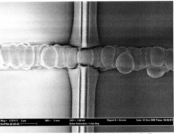
The fabrication process for the nanorelay is an adaptation of the self-aligned process proposed in [16], [17]. In this process, nickel dots are patterned on the substrate using electron beam lithography. Vertically aligned CNTs are grown from these catalyst dots using a dc plasma-enhanced chemical vapor deposition (PECVD) system. Oxide is deposited to separate the CNT from the electrical contact, which is created by depositing amorphous silicon (a-Si). Photo resist and reactive ion etching (RIE) is used to pattern the a-Si contact and release the central CNT. Figure 2-1 shows a micro ionizer that was constructed using this self-aligned process [16], [17].
Figure 2-1. SEM of self-aligned carbon nanotube-based micro ionizer [16], [17]. To modify this process to create a nanorelay, the outer circular contact must be split into two separate contacts. This is accomplished by patterning a line of carbon nanotubes, instead of a single nanotube.
The fabrication work presented in the rest of this chapter represents the combined results of a collaboration with Kaveh Milaninia. Kaveh devised the device structure and developed the initial fabrication process [28]. We were both involved the execution and debugging of the process flow, and each of us has performed all of the fabrication steps described in this chapter.
2.1 Device Design
2.1.1 Device Structure
The basic structure of the nanorelay device is shown in Figure 2-2. Two conducting contacts are patterned around a line of CNTs. The contacts are insulated from the substrate by a thin, conformal layer of silicon dioxide. When a control voltage is applied to one of the contacts, the CNTs are attracted to that contact and bend towards it. The contacts, CNTs, and substrate are all made out of a conductive material so that current can flow from either of the contacts, through the CNTs, and into the substrate. Carbon nanotubes can be very good mechanical actuators because of their flexibility and excellent current carrying capabilities [5].
Figure 2-2. 3-dimensional model of the nanorelay device.
2.1.2
Device Dimensions
Several NEMS device models have been developed in previous work [18], [19], [20], [21]. The goal of these models is to predict the dependence of the switch's I-V characteristics on the device geometry. The pull-in voltage, or the voltage when the actuator deflects and "pulls into" the contact is a primary metric for NEMS switches. The pull-in voltage is highly dependent on the switch dimensions, and so it is important to model this relationship.
Existing NEMS models were developed by adapting standard MEMS models to work at smaller dimensions [22]. In a MEMS switch, the forces acting on the actuating devices are electrostatic and elastostatic. Attractive electrostatic forces arise when a voltage is applied between the contact and the actuating device. Elastostatic forces are related to the material properties, in particular the spring factor, of the actuating device.
At the nano-scale, a third force must be considered. This force is the adhesive van der Waals force between the contact and the actuator. Van der Waals forces refer to the
attractive dipole forces between two molecules [7]. At the MEMS scale, the van der Waals forces are negligible and can be ignored. However, at the dimensions of NEMS devices, van der Waals forces have a significant effect on the system operation [23].
Using the adapted-MEMS NEMS model [18] for the nanorelay yields important information about the device operation. Figure 2-3 (a) shows all of three of the forces acting on the carbon nanotube when a voltage is applied between the substrate and one of the contacts. When the electrostatic and van der Waals forces overcome the elastostatic force, the CNT pulls-into the contact, allowing current to flow. The pull-in voltage VPI where this occurs can be related to the device dimensions by balancing the three forces at the equilibrium point:
F,1a + Felec + Fvd = 0. (2.1)
Substituting in appropriate force relationships gives
Vp,= k,g -k 2wL ( )
3 2g
, (2.2)
(g +
+
2 gWLEO
where ki and k2 are constants related to the material properties, g is the gap width, L is the
length of the CNT, d is the diameter of the CNT, and wL is the area of the side of the CNT adjusted for the circular geometry, as shown in Figure 2-3 (b) [18].
I
Hdr
(a) (b)
Figure 2-3. (a) Electrostatic, elastostatic, and van der Waals forces acting on the CNT during pull-in. (b) Nanorelay device dimensions.
Intuition about the dependence of the pull-in voltage on the device dimensions can be extracted from Equation (2.2). The pull-in voltage has a cubic dependence on the gap width g, and an inverse linear dependence on the CNT length L. Decreasing the CNT diameter d also improves the pull-in voltage by increasing the van der Waals forces. Therefore, in order to get the best pull-in performance, the nanorelay should have a high aspect ratio CNT with a minimal gap width. This pull-in voltage model gives a starting point for the device fabrication requirements and also shows that the performance of the nanorelay device improves as the dimensions scale down. In order to achieve a pull-in voltage of 5 V, the CNT should be approximately 5 pm long and the gap size should be on the order of 1 pm. For a pull in voltage of 1 V, the dimensions will have to scale to a 10 pm long CNT and a 200 nm gap size.
2.2
Carbon Nanotube Synthesis
The first step in fabricating a nanorelay is to grow a line of vertically-oriented carbon nanotubes. The PECVD system used for this process is designed to grow nanotubes vertically from a metal catalyst [24], [25], [26], [27]. This metal catalyst can be patterned using electron beam lithography in order to make the CNTs grow in specific locations. The lithography and liftoff process for patterning the catalyst and growing the CNTs is shown steps (1) - (6) of Figure 2-13.
The performance of the nanorelay is highly dependent on the dimensions and quality of the carbon nanotubes. The pull-in and pull-off voltages, switching speed, and switching reliability are all related to the CNT characteristics. In general, CNTs with a very high aspect ratio (length/diameter) provide the best performance. The dimensions of the CNTs depend on several fabrication parameters, including the growth temperature and time, and the metal catalyst material and thickness. The following subsections explore the effects of these parameters on the CNT dimensions based on experimental results.
2.2.1 Growth Temperature
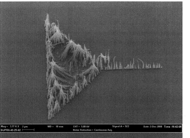
Changing the temperature of the CNT growth chamber has several effects on the CNT geometry. First, a higher growth temperature leads to longer tubes because the carbon deposition rate is increased at higher temperatures [24]. As explained in Section 2.1.2, longer CNTs are desirable because they reduce the pull-in voltage of the nanorelay. However, experimental results show that when longer CNTs are grown, the vertical uniformity suffers. After a certain length, the CNTs begin to grow in undesired directions instead of staying vertically straight.
Figure 2-4 and Figure 2-5 show the results of growth experiments at a temperature of 6750 C and 825' C, respectively. The CNTs in the 825' C experiment grew approximately four times as long as the CNTs in the 675' C experiment, but they are obviously less uniform. After approximately 2 pm of growth, the CNTs stop growing vertically and begin to branch out in unexpected directions.
Figure 2-4. CNT growth: 6750 C for 30 minutes with a 10 nm nickel catalyst.
2.2.2 Growth Time
The duration of the PECVD experiment also affects the length of the tubes, though to a lesser extent than the growth temperature. This is simply because the carbon deposition occurs for a longer time, and so the CNTs grow taller [24]. However, this trend does not continue infinitely because the total growth height is limited by the amount of metal catalyst. Once the catalyst is exhausted, the CNT growth will be unable to continue. The results of 15 minute and 30 minute growth durations are shown in Figure 2-6 and Figure 2-7, respectively. The CNTs from the 30 minute experiment are approximately
1.5 times longer than the CNTs in the 15 minute experiment.
Figure 2-7. CNT growth: 8250 C for 30 minutes with a 30 nm nickel catalyst.
2.2.3
Catalyst Material
The PECVD growth parameters are not the only factors affecting the CNT growth. The material and geometry of the metal catalyst also plays a large role in determining the geometry of the CNTs. As the PECVD system heats up, the metal catalyst dots melt and form nanospheres. The composition of the material used for the catalyst controls the formation of the nanospheres, which sets the growth rate and diameter of the CNTs [25].
Three different materials were considered for the metal catalyst. Figure 2-8, Figure 2-9, and Figure 2-10 show the forested growth results for nickel, iron, and cobalt catalysts, respectively. The nickel catalyst resulted in medium length tubes with a fairly high density. The iron catalyst yielded shorter and thinner tubes. The cobalt catalyst gave the longest tubes, at the expense of uniformity. The nickel catalyst was chosen for the nanorelay to give decently long uniform tube growth.
Figure 2-8. CNT growth: 8250 C for 30 minutes with a 10 nm nickel catalyst.
Figure 2-10. CNT growth: 8250 C for 30 minutes with a 10 nm cobalt catalyst.
2.2.4
Catalyst Thickness
The catalyst thickness affects both the diameter and length of the CNTs because the volume of the catalyst nanospheres is determined by the area and thickness of the patterned catalyst. This nanosphere volume limits the CNT dimensions [25]. Larger volumes lead to thicker, longer CNTs, while smaller volumes lead to thinner, shorter CNTs. If the volume is too large, several CNTs will grow from a single nanosphere, instead of a well-defined one-to-one CNT-to-nanosphere ratio.
Figure 2-11 and Figure 2-12 show the results of growth experiments using a 10 nm thick catalyst and a 30 nm thick catalyst, respectively. The CNTs in the 10 nm thickness experiment are evenly spaced, but short. The CNTs in the 30 nm thickness experiment are approximately 10 times longer, but multiple tubes sprout from each nanosphere, resulting in a non-uniform growth.
Figure 2-11. CNT growth: 8250 C for 30 minutes with a 10 nm nickel catalyst.
2.3 Device Fabrication
The process sequence for the nanorelay is shown in Figure 2-13. First, the metal catalyst is deposited and patterned using liftoff. Then, a line of CNTs are grown from these catalyst dots. Silicon dioxide and amorphous silicon are conformally deposited around the line of nanotubes. The amorphous silicon is patterned and etched to form contacts, and finally, the oxide is etched to release the nanotubes.
(7) Deposit oxide and amorphous Si
(8) Spin photoresist
(3) Expose PMMA using eBeam lithography
(4) Deposit thin layer of Ni
(5) Liftoff PMMA
(6) Grow CNTs
(9) Pattern contacts using lithography
(10) Etch amorphous Si using RIE
(11) Strip photoresist
(12) Etch oxide using BOE
Figure 2-13. Nanorelay fabrication process steps.
(2) Spin PMMA
This section discusses the three main fabrication challenges for constructing a nanorelay: growing a line of CNTs, forming the air gap and self-aligned contact terminals, and releasing the CNTs from the oxide. A more detailed process flow including all of the tool and material specifications is provided in Appendix A. Process Flow for Fabricating Nanorelays and [28].
2.3.1
Formation of a Line of Vertically Aligned CNTs
The line of CNTs is fabricated by patterning the location of metal dots that act as a catalyst for CNT growth. A 50 nm titanium nitride (TiN) layer is sputtered on the highly doped silicon substrate to act as a diffusion barrier for the metal catalyst. Then, catalyst dots are patterned using standard electron beam and liftoff processes. First, 4% polymethyl methacrylate (PMMA) photo resist is spun at 4000 RPM to cover the sample. This resist is exposed using electron beam lithography at 30 kV with a 20 pjm aperture and a 300 pC/cm2 dose. The resist is patterned into 5 pm long lines of 200 nm x 200 nm squares with a 400 nm pitch. The resist is developed using 2:1 isopropyl alcohol (IPA) : methyl isobutyl ketone (MIBK) for 115 seconds, and then rinsed with IPA for 1 minute.
A 30 nm thick layer of metal is deposited using electron beam evaporation at a rate of 1
A/sec and a pressure below 10-6 Torr. The PMMA is lifted off in 80°C N-methyl pyrrolidone (NMP) for 10-15 minutes. As the NMP removes the unexposed areas of PMMA, the metal that lies on top of these areas is also removed, leaving metal catalyst only in the exposed areas. This leaves a line of catalyst dots that match the electron beam lithography exposure pattern, as shown in Figure 2-14 and Figure 2-15.
Figure 2-14. Electron beam lithographically patterned Ni catalyst dots, M=3.5K X.
As mentioned in Section 2.2, multiwall carbon nanotubes are grown vertically from the metal catalyst dots using a dc PECVD system. The size and position of the CNTs are set by controlling the size and position of the metal catalyst dots, which is determined by the electron beam lithography pattern. Figure 2-16 and Figure 2-17 show a scanning electron micrograph of the line of CNTs after growth in the PECVD system.
10 pm EHT = 5.00 kV Signal A = InLens
Date :20 Nov 2008
t WD = 9.3 mm Photo No. = 5147 Time :15:37:20
Figure 2-17. Line of carbon nanotubes, tilt=30°.
2.3.2 Formation of the Gap and Contact Terminals
After the line of nanotubes has been grown, the contact structure must be formed. To prevent electrical shorts in the nanorelay, the contacts must be isolated from the silicon substrate and the CNTs. For the best performance, the gap between the contacts and the CNTs should be as small as possible. The contact structure is formed by controlling the geometries of two conformally deposited materials, the insulating silicon dioxide and the conducting amorphous silicon.
Both the silicon dioxide (SiO2) and the amorphous silicon (a-Si) are deposited using
plasma-enhanced chemical vapor deposition (PECVD) at 200'C (Figure 2-18). Approximately 1.2 pm (13 A/sec for 15 minutes) of oxide is deposited conformally over the sample. This oxide serves three purposes in the fabrication process. First, it protects the tubes from being damaged during subsequent processing steps. Second, it insulates the a-Si contacts from the conducting silicon substrate. Finally, the oxide acts as a sacrificial layer to form the space for the air gap between the contacts and the line of
CNTs. Since the oxide is conformally deposited, the gap width is equal to twice the deposited oxide thickness, or approximately 2.4 pm.
The thickness of the oxide is limited by the pitch of the line of CNTs. The oxide must be thick enough to bridge the gap between two adjacent nanotubes. Several experiments were performed to attempt to minimize this gap size in order to maximize the performance of the device.
Approximately 600 nm (4 A/sec for 25 minutes) of doped a-Si is conformally deposited for the contact material. Photolithography is used to pattern the a-Si to form the 5 pm wide lines leading to 200 pm x 200 pm square probe pads for each of the contacts (Figure 2-19). A double layer of photo resist is spun at 4000 RPM in order to planarize the photo resist. The resist is intentionally overexposed using a 6 second exposure and overdeveloped for 150 seconds so that the tops of the tubes are above the photo resist (Figure 2-20). The exposed a-Si is then etched using an electron cyclotron resonance (ECR), reactive ion etch (RIE) system (Figure 2-21). The photo resist is removed by ashing the sample, leaving a-Si contacts that go up to, but not over the top of the CNTs (Figure 2-22).
The PECVD conformal deposition allows the contact formation to be a self-aligned process, meaning that the position of the contact walls is determined by the position of the CNTs rather than using a mask alignment. This self-aligned process is imperative to the device fabrication for two reasons. First, mask alignment to the line of CNTs would be almost impossible since the width of the line is on the order of tens of nanometers. Second, having a self-aligned process allows the air gap to be as small as possible. The width of the air gap is determined by the oxide thickness, which is only limited by the spacing between the CNTs.
Figure 2-18. Line of nanotubes covered with conformal SiO2 and a-Si, tilt=30°.
Figure 2-20. Patterned photo resist, tilt=30'.
I I'MI
I
WD 71: J i :
Figure 2-22. a-Si contact after resist has been stripped, tilt=30°.
2.3.3
Release of the CNTs
As with most NEMS devices, the most delicate part of the nanorelay process is the final release of the mechanical CNT actuators. The oxide deposited over the CNTs must be removed in order to allow the CNTs to move back and forth freely between the two contacts. This final release must be carefully controlled because the CNTs are extremely fragile once the protective oxide has been removed. Furthermore, as the oxide is removed, the CNTs experience stiction forces that tend to cause them to stick together which prevents CNT actuation. Several processing techniques were investigated for the final oxide removal step, in order to obtain the best release results.
The first release technique uses a traditional buffered oxide etchant (BOE) to remove the oxide around the CNTs. The sample is submersed in a 49% hydrofluoric acid (HF) BOE solution for 60 seconds, rinsed with water, and finally blow-dried with a nitrogen gun. The advantage of this technique is that it is a well-known process for oxide
removal. However, there are three main disadvantages. First, since this technique is a wet etch, the etching is not very well controlled and can vary from sample to sample. Second, since wet etches undercut, if the sample is etched for too long, the insulating oxide between the substrate and the contacts could be inadvertently removed. Third, wet processing induces stiction in high aspect ratio structures, like CNTs. As the liquid dries, the CNTs are pulled in by the surface tension of the liquid droplets. This is especially evident in areas of forested growth, as shown in Figure 2-23, but can also affect the lines by pulling the CNTs into one of the contacts prematurely, as in Figure 2-24.
To avoid the liquid stiction forces, the nitrogen gun dry was replaced by a force hot plate dry. After the BOE and rinse steps, the sample was placed on a hot plate while it was still wet. The hotplate temperature was set well above the boiling point of water, so that the liquid would evaporate almost immediately. Unfortunately, this did not prevent the stiction forces and the CNTs were still pulled into bundles. Completed devices that used the BOE and hotplate release technique are shown in Figure 2-25 and Figure 2-26. The lines of CNTs in these devices do not appear to have been affected by stiction, but this is only because the CNTs were too short to bend. Stiction effects were seen in forested areas of the sample, and CNTs that are this short will not be able to switch in the actual device.
Figure 2-23. Forest of CNTs showing effects of stiction forces after wet etch, tilt=30°.
Figure 2-25. Completed device after BOE release, tilt=30°.
The second oxide removal technique that was attempted is a vapor HF etch. In this technique, the sample is place above a beaker of HF that is heated to 70'C. The HF vaporizes and travels up the column to the sample, where it etches the oxide. Since the HF is in vapor form, the stiction forces associated with wet etches should be eliminated. While the stiction forces were eliminated, the vapor HF process left re-deposited residue on the surface of the sample, as shown in Figure 2-27 and Figure 2-28. A completed device that used the vapor HF release technique is shown in Figure 2-29. Since the residues are located between the CNTs and the contacts, it could possibly short the device or obstruct the actuation, so the vapor HF technique was ruled out.
Figure 2-28. Line of CNTs after vapor HF release, tilt=0'.
Figure 2-29. Completed device after vapor HF release, tilt=30°.
IF-
--
jwwhA I9C3LIILL
The final release technique is a critical point dry of the sample. The critical point of a fluid is the temperature where the fluid's liquid and gas phases have the same density. Drying at the critical point allows the liquid to vaporize without creating any surface tension stiction forces that could damage the CNTs. A critical point drying system is used to implement this technique. The oxide is first etched using a BOE and rinse, as described above. Without drying, the sample is immersed in 50%, 75%, 90%, 100%, and 100% ethanol solutions for a few minutes each. This replaces the water from the BOE rinse with ethanol which has a lower critical point. The sample is then place in 100% ethanol within the critical point drying system, which heats the sample to the critical point. At this temperature, the liquid vaporizes without stiction, and the sample dries without the CNTs being pulled together.
A forested area and a line of CNTs after a critical point dry release are shown in Figure 2-30 and Figure 2-31, respectively. A completed device that used the critical point dry technique is shown in Figure 2-32. These devices showed no signs of stiction forces, but unfortunately the CNT growth and gap thickness were not uniform enough to make a functional nanorelay.
...... ... -- ...
MAq - 935 K X OiP Ii Iwo Si(joM A hil eos Date A I 1.1m XMI-I Tirne:1317:44'! :SUPRA40-25-92 Noi," Reditction Cowinuous Avil.
... ... .... ..... ...
Figure 2-30. Forest of CNTs showing no stiction effects after critical point dry, tilt=300.
Figure 2-32. Completed device after critical point dry release, tilt=30°.
Based on the results of these experiments, critical point drying is the best technique for releasing the CNTs from the oxide. Traditional wet etch processing does not work as a release technique because as the liquid evaporates, stiction forces cause the nanotubes to be pulled together. Implementing a hot plate dry after the wet etch does not alleviate this problem since the liquid still makes a transition to the gas phase. A vapor HF etch technique can be used to avoid stiction problems, but oxide can redeposit on the substrate, resulting in a nonfunctioning nanorelay. Critical point drying was shown to eliminate stiction forces without any negative consequences. This release technique takes advantage of the well-known wet etch process and preserves CNT separation by precluding the liquid to gas phase transition.
Chapter 3
3 Nanorelay Device Characterization
This chapter describes the characterization of the nanorelay device performance. At the time of publication, a perfectly fabricated nanorelay device was unavailable. These characterization measurements come from nanorelays with relatively short and non-uniform tubes. As such, these measurements should be considered as a proof-of-concept, and a starting point for the actual performance of a high-quality nanorelay.
Several test experiments were performed to evaluate the performance of the nanorelay. By controlling the applied voltage and measuring the resulting current, a characteristic I-V curve can be obtained. This I-V relationship can be used to observe device functionality, as well as quantify the pull-in voltage and contact resistance of the nanorelay. These experiments demonstrate single switching and show that the nanorelay is able to reliably conduct current after pull-in.
3.1 Experimental Setup
The characterization measurements were taken using a Keithley Instruments parametric test system. Test probes were used to connect the Keithley's terminals to the contact pads of the nanorelay device. All measurements were performed inside of a scanning electron microscope (SEM) so that the device would be under vacuum and so the CNT switching could be visibly observed. The Keithley was used to control the applied voltage between the contact and the substrate while measuring the current flow through the switch in order to obtain I-V characteristic curves for the nanorelay device.
3.2 Pull-in Voltage
Figure 3-1 shows measured I-V data for a single nanorelay switch. During the first run, as the voltage is ramped up no current is measured until a sudden jump around 12.5 V. This point indicates where the CNT pulled-into the contact and started conducting current.
Before pull-in, the current reading is dominated by measurement noise, showing that the off-state leakage current of the nanorelay is extremely small. After pull-in, the current through the nanorelay increases to 2 nA, and continues to increase as the voltage increases, indicating a simple on-resistance model.
During the second run, there is no apparent pull-in point, and the nanorelay conducts current at low voltages. This occurs because the nanorelay is deliberately not pulled-off of the contact between experiment runs, so it acts as a short circuit between the contact and the substrate. This demonstrates the non-volatile nature of the nanorelay; when the supply voltage is removed, the CNT is held in place by the adhesive van der Waals forces, which holds the state of the switch.
A pull-in voltage of 12.5 V is relatively low for a NEMS switch [8], [9], [20], [29], [30], and is considered a promising result considering the fact that this measurement was taken using a low-quality nanorelay. Furthermore, the pull-in voltage improves dramatically as the device scales to smaller dimensions, as explained in Section 2.1.2. The major barrier to decreasing the pull-in voltage to be compatible with scaled CMOS technologies is the gap size. To achieve pull-in at 1 V, the gap size must be decreased from 2 pm to 100 nm, which is a factor of 20. In order to decrease the gap size this drastically, it will be necessary to have better control over the growth density of the line of CNTs.
S--Run 1 -Run 2 -2 -3 -15 -13 -11 -9 -7 -5 -3 -1 Voltage (V)
Figure 3-1. Measured I-V data for a fabricated nanorelay device. Run 1 shows the pull-in voltage of 12.5 V, Run 2 shows that the CNT stayed on the contact after the control voltage was removed.
3.3 On-Resistance
The I-V characteristic curves can also be used to determine the on-resistance of the nanorelay. Figure 3-2 shows the measured I-V data for several nanorelay devices in the on-state. The on-resistance of the devices can be extracted from this data as
AV
Ro = (3.1)
S AI
These measurements yield an average on-resistance of approximately 600 MQ, which is on the same order of magnitude of other NEMS switches [8], [29], [31]. However, when compared to CMOS technologies, this on-resistance is extremely high. In order to use the nanorelay in conjunction with CMOS technologies, it will be necessary to reduce this on-resistance.
A short-term solution to this problem is to place many nanorelays in parallel to reduce the equivalent on-resistance of the overall switch. This will also increase the current carrying capabilities of the switch by providing more CNTs to share the current load. The area
overhead of this solution should not be a large problem since the vertical structure of the nanorelay is area-efficient. In order to further improve the on-resistance of a single nanorelay, it will be necessary to adjust the fabrication process. The on-resistance of the nanorelay is dominated by the contact resistance of the connection between the nanotube and the contact terminal. This resistance could possibly be improved by using different materials for the metal contacts to attempt to create a more ohmic contact [32].
2 0 -2 o--Dev 5 -6 -D-8ev -10 -25 -20 -15 -10 -5 0 Voltage (V)
Figure 3-2. Measured I-V data for fabricated nanorelay devices in the on-state showing an average contact resistance of 600 MO.
Chapter 4
4 Low-Power Circuit Applications and CMOS
Test Chip
The measured I-V characteristics show that a high-quality nanorelay has many potential applications in CMOS circuit design. The main advantage of the nanorelay is its very low leakage current, which makes it ideal for use in low-power designs. Another advantage is its nonvolatile operation, which is useful in nonvolatile memory applications. This chapter explores several circuit applications that take advantage of the nanorelay's unique properties. Three of these circuits, power gating, nonvolatile SRAM, and reconfigurable interconnect, are implemented in a foundry fabricated CMOS test chip to quantify the benefits of using nanorelays in conjunction with CMOS circuits. The simulation results presented in this chapter are based off of RC extracted layout from the CMOS test chip.
4.1 Circuit Applications
4.1.1 Power Gating
One of the main potential advantages of the nanorelay is that it should effectively eliminate leakage currents because it has a physical gap tunneling barrier. An application that takes advantage of this property is power gating for digital CMOS circuit blocks. Figure 4-1 shows an example of a nanorelay power gating a single CMOS inverter. The nanorelay is used as a power footer that separates the CMOS inverter from the low supply voltage (usually ground). During normal operation, the nanorelay acts as a short circuit between true ground and a virtual ground node, as shown in Figure 4-1 (a). During idle mode, the nanorelay disconnects the virtual ground node to eliminate leakage currents, as shown in Figure 4-1 (b).
VDD VDD
Leak = 0
Vss
Vss
(a) (b)
Figure 4-1. Nanorelay used as a power footer during (a) active mode, and (b) idle mode. Power gating is an ideal application for demonstrating how nanorelays can be used to improve existing CMOS circuit designs. The load circuit is unaltered, and is still implemented using CMOS technologies, which has many advantages including speed, reliability, and being a mature, well-understood technology. When nanorelays are added as power footers, they provide the additional advantage of low-leakage, which decreases the overall power consumption. One possible drawback of this power gating design is the on-resistance drop between the true and virtual ground nodes. As mentioned previously, the device on-resistance could possibly be improved through fabrication adjustments, but in the short-term this problem can be avoided by connecting many nanorelays in parallel to reduce the overall equivalent resistance.
For this type of power gating to be worthwhile, the leakage energy saved during the idle state must be greater than the energy required to recover from idle mode. The recovery energy is determined by the energy used to switch the nanorelay, Eswitch, and the energy needed to charge the virtual supply node back to VDD or GND, Echarge. The leakage energy, Eleak, is proportional to the amount of time the circuit remains in the idle state. The point in time where the leakage energy is equal to the recovery energy is called the
break even time, meaning that the circuit must be idle for at least this long for any energy to be saved [33].
The importance of the break even time is illustrated in Figure 4-2 and Figure 4-3, which show Ultrasim simulation results of power gating for different idle times. In these simulations, the nanorelay power header is controlled by a 50% duty cycle clock, as in Figure 4-4. The clock period is varied to change the amount of time that the load circuit is power gated. During the first half cycle, the nanorelay connects the power supply to the load circuit, so the load supply voltage and the consumed energy are the both the same with and without power gating. At time T/2, the nanorelay disconnects the power supply from the load, and the virtual supply voltage drops towards zero. During this time, the power gated load has no leakage, and so it does not consume any energy during the second half of the clock period. However, at the end of the period, the virtual supply node must be recharged to VDD, which requires a relatively large amount of energy. For the total energy to be less than in the case without power gating, this recharging energy
must be less than half a cycle of leakage energy, which occurs at the break even time.
Figure 4-2 shows what happens when the load circuit is power gated for less than the break even time with Ta/2 < tbe. Not enough leakage energy is saved during power gating
to overcome the energy overhead of recharging the virtual supply. Figure 4-3 shows the opposite case of power gating for longer than the break even time with T,/2 > tbe. Since the circuit is power gated for a much longer time, the total leakage energy saved is larger than the recovery energy, resulting in a lower total energy than the non-power gated case. These two simulations illustrate cases where the idle time is less than or greater than the break even time, or T,/2 < tbe < Tb/2. When the period matches the break even time, T/2
= tbe, the recovery and leakage energies will be matched, and the total energy consumed with and without power gating will be equal.
T /2 < Break Even Time a 1.5 [ 0.5 k Ta/2 Ta x 10-10 without PG with PG Ta/2 T Ta/2 TA Time
Figure 4-2. Simulation of power gating with idle time < break even time.
Tb/2 > Break Even Time 2 0 1.5, > 1 0 0.5 0 0 Tb/2 Tb x 10 -10 4 3 without PG with PG 1 S2-0 0 Tb/2 Tb Time
Figure 4-3. Simulation of power gating with idle time > break even time. 0.5
At the break even time, the relationship between the leakage and the recovery energies is given as
Eleak =recove
(4.1) Eleak = Eswitch +Echarge'
This energy relationship can be converted to the power domain by considering the amount of time the circuit is in each state. First, the nanorelay is set to switch using a clock with period T and a 50% duty cycle, as shown in Figure 4-4. The leakage energy saved by power gating occurs over half a period, when the nanorelay is disconnected from the circuit,
T
Eleak Peak - (4.2)
The energy required to switch the nanorelay must be considered over the entire period and can be expressed as
Eswitch = PswithT. (4.3)
The energy required to recharge the virtual supply node is related to the energy consumed by the load through Vload in Figure 4-4 as well as the leakage energy. The energy consumed by the load over the entire period is the energy required to recharge the node plus half a cycle of leakage while the load is not power gated,
Echarge Eload -Eleak
T (4.4)
charge -load - Pleak 2
Substituting these expressions into Equation (4.1) gives
T PT
-Peak - Pswitch + P leak xT
2 2 (4.5)
Vswitch Vload Vswitch
FL
_L
0F
L-
Load Circuit
16-bit Adder
Figure 4-4. Schematic diagram of circuit used for break even time simulation. To illustrate these relationships, simulations of the break even time were performed for power gating a 16-bit adder. The simulation results showed that the power required to switch the nanorelay, Pswitch, is very low when compared to the power required to
recharge the virtual supply node, Ph,,arge. As a result, the break even time is mostly determined by the characteristics of the load circuit; more leakage results in a smaller break even time. Figure 4-6 and Figure 4-5 summarize the break even time simulation results in the power and energy domains, respectively. For a 16-bit adder in a 0.18 pm process, the break even time was 48 ps, at scaled technology nodes where there is more


![Figure 2-1. SEM of self-aligned carbon nanotube-based micro ionizer [16], [17].](https://thumb-eu.123doks.com/thumbv2/123doknet/14200915.479939/19.918.212.724.556.966/figure-sem-aligned-carbon-nanotube-based-micro-ionizer.webp)