Degree Programme
Systems Engineering
Major Infotronics
Bachelor’s thesis
Diploma 2017
Joel Bodenmann
2
2
D
D
H
H
a
a
r
r
d
d
w
w
a
a
r
r
e
e
A
A
c
c
c
c
e
e
l
l
e
e
r
r
a
a
t
t
i
i
o
o
n
n
Professor F r a n ç o is C o r t h a y Expert Ya n n T h o m aSubmission date of the report
This document is the original report written by the student. It wasn’t corrected and may contain inaccuracies and errors.
Objectives
The objective of the project is to develop an IP-core that provides hardware acceleration for common 2D rendering operations in an embedded system.
Methods | Experien ces | Resu lts
The requirements for graphical user interfaces (GUI) on modern display and touchscreen based systems are increasing steadily. Rendering complex and attractive GUIs requires a lot of processing power. At the same time, energy consumption for most of these embedded systems should decrease. Being able to off-load processor intensive tasks such as rendering of 2D shapes to dedicated hardware vastly decreases rendering time and frees a lot of processor resources which leads to a faster GUI and a less power consuming system.
Existing solutions often work only under very strict conditions and with specific platforms and are not flexible enough for the demands of the µGFX library which has been designed to run on virtually any system.
The result of the project is a ready-to-use IP-core that provides hardware acceleration for rendering solid rectangles in a NIOS-II based system. The design can be adapted to be used in any system. New hardware renderers for additional shapes can be added easily without modifying the rest of the design.
2D rendering with hardware acceleration
Graduate
Joel Bodenmann
Bachelor’s Thesis
| 2 0 1 7 |
Degree programme Systems engineering Field of application Infotronics Supervising professor Dr François Corthay [email protected] Partner uGFX GmbH https://ugfx.ioThe “drawing infinitely many
rectangles” to confirm the stability of
the Silizium IP-core and to demonstrate the speed improvement.
A typical graphical user interface on an embedded system running NIOS-II and the µGFX library.
Picture
(optional)
300 dpi
6.5 x 5cm
Picture
(optional)
300 dpi
6.5 x 5cm
Objectif du projet
L'objectif du projet est de développer un coeur IP qui fournit une accélération matérielle pour les opérations de rendu graphique en 2D dans un système embarqué.
Méthodes | Expérie nces | R ésultats
Les exigences pour les interfaces utilisateur graphiques (graphical user interface / GUI) sur l'affichage moderne des systèmes à écran tactile augmentent régulièrement. Le rendu visuel des interfaces graphiques complexes et attrayantes nécessite beaucoup de puissance de traitement. En même temps, la consommation d'énergie de la plupart de ces systèmes embarqués est censée diminuer. Le fait de pouvoir décharger les tâches intensives du processeur telles que le rendu des formes 2D sur un circuit dédié diminue considérablement le temps de dessin et libère beaucoup de ressources du processeur. Ceci nous conduit à une interface graphique plus rapide et à un système moins consommateur d'énergie.
Les solutions existantes ne fonctionnent souvent que dans des conditions très strictes et sur des plates-formes spécifiques. Elles ne sont pas suffisamment souples pour répondre aux exigences de la bibliothèque μGFX qui a été conçue pour fonctionner sur pratiquement n'importe quel système.
Le résultat du projet est un coeur IP prêt à l'emploi qui fournit une accélération matérielle pour le dessin de rectangles solides dans un système basé sur NIOS-II. Le circuit peut être adapté pour être utilisé dans n'importe quel système. De nouveaux calculateurs matériels pour des formes supplémentaires peuvent être ajoutés facilement sans modifier le reste de la conception.
Rendu en 2D avec accélération matérielle
Dip lômant
Joel Bodenmann
Trava il de dip lôme
| é d i t i o n 2 0 1 7 |
Filière Systèmes industriels Domaine d’application Infotronique Professeur responsable Dr François Corthay [email protected] Partenaire uGFX Sarl https://ugfx.ioLe «dessin d'infiniment de rectangles» pour confirmer la stabilité du coeur IP Silizium et pour démontrer l'amélioration de la vitesse.
Une interface utilisateur graphique typique sur un système embarqué fonctionnant avec NIOS-II et la bibliothèque μGFX.
Page 1 of 39
Table of Contents
1 Preamble ... 3 2 Motivation ... 3 3 Project goal ... 3 4 Document structure ... 45 Terms & abbreviations ... 4
6 Technical advantages ... 5
6.1 Example 1: Image blitting ... 5
6.2 Example 2: Area filling ... 6
7 Used tools ... 7
8 QSys ... 7
8.1 Avalon ... 8
9 Simplifications ... 8
10 Hardware acceleration features ... 8
11 Architecture ... 10
12 Internal design ... 12
12.1 Command & Control bus interface ... 12
12.2 Registers ... 12 12.3 Command FIFO ... 12 12.4 Dispatcher ... 14 12.5 Framebuffer interface ... 14 12.5.1 Write ... 16 12.5.2 Read ... 17 12.5.3 Clipping ... 18
12.5.4 Read and write FIFO ... 19
12.5.5 FIFO data format ... 20
12.6 Renderers ... 23 12.6.1 Pixel ... 23 12.6.2 Filled rectangle ... 23 12.6.3 Clipping ... 24 13 Implementation ... 24 13.1 Silizium.vhd ... 25 13.2 Silizium_implementation.vhd ... 26 13.3 Silizium_dispatcher.vhd ... 27 13.4 Silizium_framebufferinterface.vhd ... 28
Page 2 of 39
14 Adding new renderers... 30
14.1 Generics ... 30
14.2 Ports ... 30
14.3 Infrastructure ... 31
15 Tests & Verification ... 32
16 Future steps ... 33
16.1 More hardware renderers ... 33
16.2 Test benches ... 33
16.3 FIFO abstractions ... 33
16.4 Bus abstractions ... 34
16.5 Clipping ... 34
16.6 Framebuffer interface burst transactions ... 34
17 Parallel Rendering ... 34
17.1 Framebuffer interface bottleneck... 34
17.2 Synchronization... 35 18 Problems ... 35 18.1 Framebuffer interface ... 35 18.2 Missing pixels ... 36 19 Conclusion ... 36 20 Signatures ... 37 21 Credits ... 37 22 Appendix ... 37 23 Bibliography ... 38 24 List of illustrations ... 39 25 List of tables ... 39
Page 3 of 39
1 Preamble
This is the official and final report for the bachelor thesis.
2 Motivation
This project has been proposed as a bachelor thesis by myself. As the author and maintainer of the µGFX1 library I know how many CPU resources rendering even simple shapes such as a solid rectangle
can take. On small microcontroller systems or FPGAs with soft-cores this is usually a big problem as these CPUs are not only comparably slow but also need to take care of a magnitude of other things such as processing user events or handling wireless communication which often involve hard-realtime requirements. These hard-realtime requirements often require the 2D rendering tasks to be split up into multiple different operations which makes rendering a user interface even slower and therefore quickly leads to a non-smooth user interface which does not hold up to the ever-growing performance demands of modern graphical user interfaces.
Being able to off-load even simple tasks such as rendering a filled rectangle to a dedicated part of the hardware (GPU) doesn’t only vastly increase rendering speed but also frees up a lot of CPU resources. Dedicated hardware to off-load rendering operations for smaller systems is nothing new. There are several display controllers such as the RA8875 from RAiO which provide hardware support for rendering basic 2D shapes. Furthermore, there are more complex systems such as the FT800 from FTDI which implement hardware rendering for complex shapes and widgets such as pushbuttons, sliders and even entire on-screen keyboards. More advanced microcontrollers that feature built-in display controllers also start to provide very basic hardware acceleration support for rectangle drawing and other basic operations such as the LTDC display controller that can be found in some of the higher-end STM32 microcontrollers. These existing solutions tend to be very inflexible and are always highly proprietary. They can almost always only be used with the matching closed-source software of the vendor or they come with other restrictions that vastly limit the field of use. The goal of this project is to develop a system that can be integrated easily into any existing and new system.
3 Project goal
The goal of this thesis is to develop an IP-core that provides 2D hardware acceleration to a system-on-chip2 (SoC) to speed up graphical user interfaces on embedded systems.
More specifically, the IP-core will be implemented in VHDL3 and will be optimized for the use with the
µGFX library and the NIOS-II4 processor.
While we will refer to this IP-core as “a GPU” (graphical processing unit) it is not to be compared to a traditional GPU of a desktop computer system. The goal of this project is to implement hardware 2D acceleration for small embedded systems that do not require fancy animations or 3D renderings. The
1 https://ugfx.io
2 https://en.wikipedia.org/wiki/System_on_a_chip 3 https://en.wikipedia.org/wiki/VHDL
Page 4 of 39 GPU will be optimized to be small & simple and also easy to use for the CPU as we want to save as much CPU time as possible on those smaller low-performance systems.
4 Document structure
The complete bachelor thesis report consists of three separate documents: • The actual report itself (this document)
• The datasheet of the developed IP-Core
• A document that describes the problem that was faced when implementing the Avalon-MM master bus interface
These three documents refer to each other were necessary. To a person unfamiliar with the project it is best to start with the datasheet and then moving on to reading the rest of this report.
The reason for having a separate document regarding the problem with the Avalon-MM master bus interface is that the problem has not been solved yet. A workaround that is suitable to finish this thesis has been found and applied but solving the problem has yet to be done.
5 Terms & abbreviations
The following table gives an overview of terms and abbreviations that are commonly used throughout this document:
Abbreviation Description
2D Two dimensional
Avalon A bus standard created by Altera for FPGA internal communication CPU Central processing unit
FBI Framebuffer interface
FIFO First-in First-out (a type of memory/buffer)
Framebuffer A section of memory that holds the pixel data that is shown on the display FSM Finite state machine
GPU Graphics processing unit HAL Hardware abstraction layer
IP-Core (Intellectual property) A pre-fabricated block of something ready to be used Qsys Tool of the Quartus toolchain used to create a SoC
Quartus The FPGA IDE & Toolchain by Intel
Silizium The name of this 2D hardware acceleration IP-Core SoC System-on-chip
Page 5 of 39
6 Technical advantages
This section of the document explains the technical advantages of having dedicated hardware for 2D rendering operations. This is basically the technical variant of section 2 (motivation). This section assumes that the reader is familiar with the basic concepts of a computer system (especially the CPU). A CPU is usually designed to be very good at executing a broad variety of different tasks (tasks in terms of logical operations and bit operations which together form calculations). Just as with most other things, when something is designed to be usable for many different things it is usually not very good at one particular thing. While a CPU offers everything required to render two dimensional shapes such as rectangles and polygons or to copy images around, it is not really optimized for that. This section of the document contains two examples that will illustrate why having dedicated hardware for 2D rendering operations can be a huge benefit in terms of the overall application speed.
6.1 Example 1: Image blitting
Blitting (historically also known as bit blit) stands for bit block transfer and describes a technique to assemble a bitmap (ultimately an image) from different parts of multiple different images. In layman’s terms, it’s taking a region of pixels and copying to a different location. A good example is rendering an image: When the developer of an (embedded) GUI wants to show an image on the display said image needs to be loaded from memory (eg. an SD-Card). Afterwards, the image needs to be decoded (usually by the CPU) and gets cached (“stored temporarily”) into memory. The cached version of this image is somewhere in memory but not inside the framebuffer. This means that the image is fully rendered but simply not on the display yet. Therefore, the next operation is to create a copy of the cached (decoded) image in memory. Copying memory is a very inefficient task for a CPU. To copy memory, a CPU must read a chunk of memory and store it in its internal registers and then write it back to a different memory location. As those registers are usually just big enough for a few bytes (eg. 32 to 48 bytes in a typical modern microcontroller CPU) a lot of those read-store-write transactions need to be executed to copy a rendered image which often takes 2 to 4 bytes of memory per pixel. Each of those read-store-write transactions comes with overhead and also keeps the CPU from doing anything else. Assuming a small icon of 64 x 64 pixels size with a color format that takes 4 bytes per pixel it would take a CPU with the ability to store 32 bytes in registers at once 512 of those transactions:
𝑛𝑢𝑚𝑏𝑒𝑟 𝑜𝑓 𝑡𝑟𝑎𝑛𝑠𝑎𝑐𝑡𝑖𝑜𝑛𝑠 = 64 ∗ 64 ∗ 4 𝑏𝑦𝑡𝑒𝑠
32 𝑏𝑦𝑡𝑒𝑠 = 512
Almost all embedded systems (such as microcontroller) which would be used to implement graphical user interface offer DMA5 (direct memory access) which is a part of dedicated hardware next to the
CPU that allows copying memory without using/occupying the CPU. However, those DMAs cannot be used efficiently in such an application as they only support linear memory spaces. Copying a two-dimensional object in a framebuffer requires to wrap at the end of the object and then move to a different starting address for the next row. Traditionally DMAs cannot do this as they only provide a start and end address configuration parameter and constantly increment between the two. Therefore, a CPU would have to setup the DMA to copy one row of the image, wait for it to finish and then configure it to copy the next row.
Page 6 of 39 A hardware blitting engine is basically a DMA that knows the concept of having two-dimensional information in a linear memory space (a framebuffer). Instead of a start and stop address it gets provided with the start address and the width and height of the object in pixels. There are two benefits of having dedicated hardware for this:
• This dedicated hardware will be a lot faster at copying that memory (as it has been built especially for this task)
• After configuring and starting the hardware blitting engine the CPU can occupy itself with other things such as reacting on user inputs or decoding the next resource (eg. image) that will be used
These two benefits combined speed up the final application a lot as the operation of copying the image is faster and the latency to react on user input and similar decreases at the same time.
While the latest and most high-end microcontrollers such as some of the STM32 F4 and F7 series microcontrollers are equipped with such a DMA2D it is still rarely the case and in all cases those two-dimensional DMAs are only able to be used together with the built-in display controller of those microcontroller which in turn imply a large set of new limitations.
6.2 Example 2: Area filling
In the first example, the main argument for having a dedicated piece of hardware was that a CPU is a lot slower at copying memory around than dedicated hardware that has been optimized for this. As the dedicated hardware is a lot faster performing the same operation the time required to perform the copying operation drops down. However, there are also cases where the CPU itself would be fast enough to perform the job but having dedicated hardware still saves overall time because the CPU can perform other tasks in the meantime. A good & easy to understand example for this is area filling (rendering a filled rectangle in the framebuffer). Ultimately, the value of each pixel in the framebuffer needs to be modified. A (modern) CPU is not a whole not slower at this compared to dedicated hardware but when the CPU can off-load this task to dedicated hardware the CPU has time to perform other tasks.
The two examples above illustrate why and how dedicated hardware for 2D rendering operations can vastly speed up graphical user interfaces.
Page 7 of 39
7 Used tools
The overall goal of this project is to develop an IP-core that can be used in any system afterwards. However, for the scope of this bachelor thesis project we will focus on implementing a design that runs on a MAX10 FPGA using the NIOS-II system. The following tools are used to achieve that goal: Software
• Quartus 17.0 (Quartus Prime Version 17.0.0 Build 595 04/25/2017 SJ Standard Edition) • Eclipse for NIOS-II Kepler Service Revision 2, Build 20140224-0627
• ModelSim Intel FPGA starter edition 10.5b (Revision 2016.10) • µGFX library v2.7
Hardware
• Terasic MAX10 Neek6
8 QSys
A NIOS-II based system is usually developed using a utility named QSys7 that is part of Intels FPGA
development suite named Quartus8. QSys provides a graphical interface for designing a SoC. As the
2D hardware acceleration IP-core would be part of the resulting SoC it is essential that the developed block can be added easily to a QSys project through the graphical user interface.
Figure 1: QSys screenshot
6 https://www.terasic.com.tw/cgi-bin/page/archive.pl?Language=English&No=956
7 https://www.altera.com/products/design-software/fpga-design/quartus-prime/features/qts-qsys.html 8 https://en.wikipedia.org/wiki/Altera_Quartus
Page 8 of 39
8.1 Avalon
The IP-core that provides the hardware accelerations needs an interface through which it can communicate with the CPU. The NIOS-II CPU relies heavily on the Avalon bus9, specifically the Avalon
memory mapped (Avalon-MM) bus. The Avalon-MM bus offers a master-slave topology with multi-master capabilities. Our IP-core will have an Avalon-MM bus slave through which the CPU can send commands to the GPU. Furthermore, the GPU will also feature an Avalon-MM bus master that allows accessing the framebuffer.
9 Simplifications
Due to time limitations, the following decisions have been made to keep the design simpler: • No parallel rendering
After identifying the resources & systems that will be used and after deciding which simplifications are being made for the scope of this bachelor thesis it is time to determine which functions bring the most benefits when implemented in hardware.
10 Hardware acceleration features
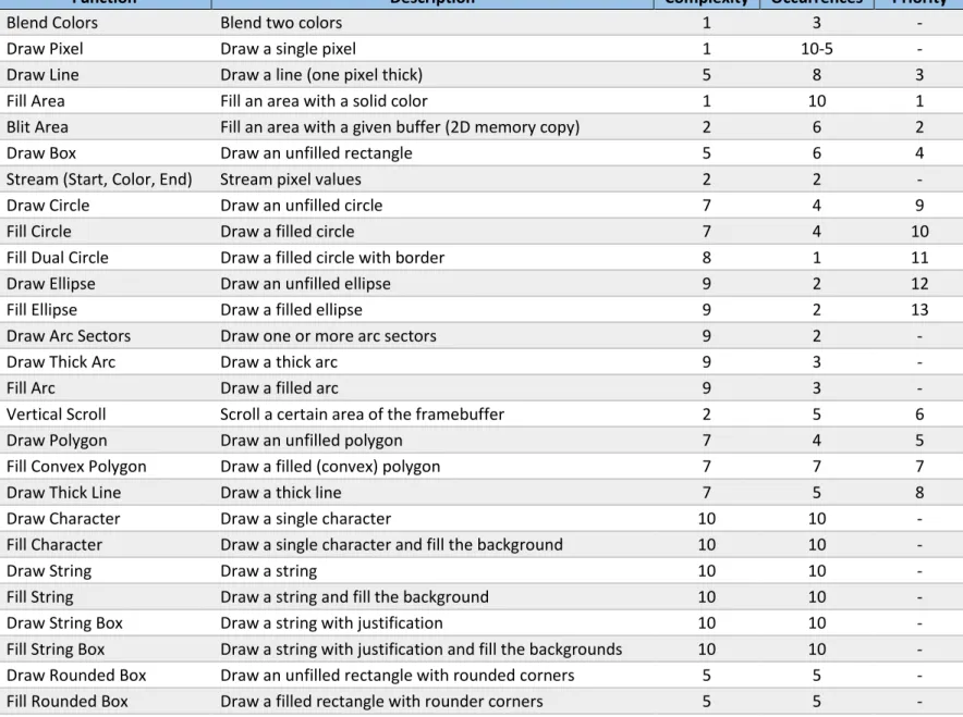
A crucial step of the project is to identify which rendering functions bring the most benefits when implemented in hardware. For this, Table 2 has been created that lists the basic rendering functions provided by the µGFX library together with a rating of their complexity (in terms of implementation) and how often they are used in a typical application. From those two values, a priority rating has been deduced from which in turn the order of implementation for this project has been deduced.
Column description:
• Complexity: The complexity of the existing software algorithm relative to all other rendering algorithms in the table. 10 is the most complex.
• Occurrences: The number of occurrences in a practical real-world GUI implementation relative to all other rendering algorithms in that table. 10 is the most used one.
• Priority: The priority in terms of order of implementation for this thesis/project.
The complete API reference for all primitive rendering functions that the µGFX library provides can be found here: http://api.ugfx.io/group___g_d_i_s_p.html
Page 9 of 39
Function Description Complexity Occurrences Priority
Blend Colors Blend two colors 1 3 -
Draw Pixel Draw a single pixel 1 10-5 -
Draw Line Draw a line (one pixel thick) 5 8 3
Fill Area Fill an area with a solid color 1 10 1
Blit Area Fill an area with a given buffer (2D memory copy) 2 6 2
Draw Box Draw an unfilled rectangle 5 6 4
Stream (Start, Color, End) Stream pixel values 2 2 -
Draw Circle Draw an unfilled circle 7 4 9
Fill Circle Draw a filled circle 7 4 10
Fill Dual Circle Draw a filled circle with border 8 1 11
Draw Ellipse Draw an unfilled ellipse 9 2 12
Fill Ellipse Draw a filled ellipse 9 2 13
Draw Arc Sectors Draw one or more arc sectors 9 2 -
Draw Thick Arc Draw a thick arc 9 3 -
Fill Arc Draw a filled arc 9 3 -
Vertical Scroll Scroll a certain area of the framebuffer 2 5 6
Draw Polygon Draw an unfilled polygon 7 4 5
Fill Convex Polygon Draw a filled (convex) polygon 7 7 7
Draw Thick Line Draw a thick line 7 5 8
Draw Character Draw a single character 10 10 -
Fill Character Draw a single character and fill the background 10 10 -
Draw String Draw a string 10 10 -
Fill String Draw a string and fill the background 10 10 -
Draw String Box Draw a string with justification 10 10 -
Fill String Box Draw a string with justification and fill the backgrounds 10 10 - Draw Rounded Box Draw an unfilled rectangle with rounded corners 5 5 - Fill Rounded Box Draw a filled rectangle with rounder corners 5 5 -
Page 10 of 39
11 Architecture
Initially the idea was to create one IP-core per hardware acceleration function. However, after reading a lot of material about QSys it became clear that the best solution is to create just one IP-core that internally dispatches the jobs to the different sub components. The reason for this is that all of these components would require the same bus interface which would result in a lot of code duplication and would also require the user of the IP-core to hook up each block manually which quickly becomes a tedious task with a growing number of renderers and also decreases readability of the overall SoC design. Furthermore, the QSys tool provides a nice graphical configuration dialog for each IP-core. Once the Silizium IP-core is completed we can create a configuration dialog where each hardware acceleration feature can be either enabled or disabled and further configured. Another advantage of having just one IP-core is that we can handle the bus arbitration internally ourselves. This allows for further optimizations such as running multiple different rendering jobs in parallel, optimizing for burst transactions and similar.
From the end user’s perspective, there will be just one IP-core with one Avalon-MM slave and one Avalon-MM master interface:
2D Hardware Acceleration Avalon-MM Slave Avalon-MM Master 2D Hardware Acceleration Avalon-MM Slave Avalon-MM Master Figure 2: IP core interfaces
The slave interface will be used to configure and control the GPU as well as issuing rendering commands. The master interface is used to access the framebuffer memory.
Figure 3 shows two different use cases for the Silizium IP-core in a typical NIOS-II based SoC. It is to note that the Silizium block is not affected by other aspects of the systems such as the location of the framebuffer (eg. Internal or external memory) or the used display interface.
Page 11 of 39 CPU Framebuffer Reader Avalon-MM RAM Interface S RAM Interface S M Silizium S M M Clocked Video Output CPU Framebuffer Reader Avalon-MM RAM Interface S M Silizium S M M Clocked Video Output FPGA Display CPU Framebuffer Bridge Avalon-MM RAM Interface S M Silizium S M M FPGA Display External RAM External RAM
Note: RAM Interface could be internal RAM as well depending on the system architecture
Framebuffer Framebuffer
Page 12 of 39
12 Internal design
Figure 4 gives an overview of the internal design of the Silizium IP-core. The design can be split into the following components:
• Command & Control bus interface • Registers
• Command FIFO • Dispatcher • Renderers
• Framebuffer interface
Note: The purpose of said figure is to give an overview of how things work internally. The actual implementation is split up into different entities.
12.1 Command & Control bus interface
The command & control bus interface (from here on referred to as “the slave interface”) is used by the CPU to initialize, configure and control the GPU. The interface is compliant to the Avalon-MM slave standard and has the following requirements:
• Address bus width: At least 4 bits • Data bus width: At least 32 bits • Read and write operations
The run-time configuration of the GPU usually only consists of setting the framebuffer base address and the framebuffer span. Other parameters such as the display size, the pixel format and similar are handled by generic values and therefore do not need to be changed during run-time. Once the configuration is completed the slave interface is usually only used to send commands to the GPU, to control the different enable flags (if required) and to read back the current status of the GPU (eg. busy flags) and the command queue status.
12.2 Registers
The GPU features different control and configuration registers. The most important ones are: • Status register
• Control register
• Framebuffer base address & span register
These registers can be accessed directly via the slave interface.
The documentation of the values and effects of these registers are documented in the datasheet.
12.3 Command FIFO
The CPU issues commands to the GPU such as “draw a rectangle at this position with that size and this color”. These commands are stocked in the internal command FIFO of the GPU. Whenever there is a pending command in the FIFO the dispatcher will grab it as soon as the different renderers of the GPU are no longer busy and handle it accordingly.
Page 13 of 39 Renderer 1 Registers ... ... ... Param 1 Command 3 Param 4 Param 3 Param 2 Param 1 Command 2 Param 3 Param 2 Param 1 Command 1 Dispatcher Control Status FB Base Addr FB Span FIFO Fr am eb uf fer A cc es s M ux Renderer 2 Renderer 3 Renderer 4 Renderer 5 FB Interface Avalon-MM Master FB Interface Avalon-MM Master
Slave Bus Interface
Avalon-MM Slave
Slave Bus Interface
Avalon-MM Slave Se le ct o r
Page 14 of 39
12.4 Dispatcher
The dispatcher takes commands out of the command FIFO and dispatches them to the appropriate hardware rendering blocks. To fulfill that task, the dispatcher also handles the internal bus arbitration and parallel rendering in the future (not implemented yet).
12.5 Framebuffer interface
The framebuffer interface (FBI) is the sub-component which actually talks to the framebuffer. In this particular project, we’re focusing on a NIOS-II system with a framebuffer that is accessible over an Avalon-MM bus. However, adapting to a different system is very easy.
Figure 5 gives a detailed overview of the architecture of the framebuffer interface. The left side is the communication towards the individual renderers and the right side is the communication towards the Avalon-MM bus. The first thing to note is that the framebuffer interface allows for bidirectional communication. This is due to the fact that some renderers require read-back from the framebuffer to fulfill their tasks. A common example is a hardware renderer for scrolling: Such a block takes a portion of the display contents and moves it inside the framebuffer. For this, the block needs to read the contents of the framebuffer first. Furthermore, read-back is also required for anti-aliasing and loading miscellaneous contents from other parts of the memory (off-screen memory) which is often used to store decoded images or complex pre-rendered shapes that just need to be copied to the on-screen portion of the framebuffer.
The communication towards the renderers is being buffered through two individual FIFOs: A write-FIFO and a read-write-FIFO. There are two benefits of having buffers at this place: Firstly, a renderer can keep rendering when the bus towards the framebuffer (the Avalon-MM bus) is currently being locked by another bus member. Secondly, having a write queue the framebuffer interface logic (the state machine) can optimize bus transfers by making use of burst writes (currently not implemented).
Page 15 of 39 FIFO n FIFO n-1 FIFO n-2 ... ... ... ... ... ... ... ... FIFO 3 FIFO 2 FIFO 1 Write FIFO FIFO n FIFO n-1 FIFO n-2 ... ... ... ... ... ... ... ... FIFO 3 FIFO 2 FIFO 1 Write FIFO
>=
Finite State MachineFIFO n FIFO n-1 ... FIFO 2 FIFO 1 Read FIFO FIFO n FIFO n-1 ... FIFO 2 FIFO 1 Read FIFO
FB Span FB Base Addr
Avalon-MM Master Avalon-MM Master Raw D/C Flag FB write data FB write addr FB read addr FB read data Clipping Mask Comp. Clipping Info Glue Logic Glue Logic
Page 16 of 39
12.5.1 Write
At the very basic requirements, a renderer would simply provide the framebuffer interface with an address inside of the framebuffer area and a matching value to write there. The framebuffer interface would then take care of issuing the correct write transaction on the Avalon-MM bus. There are two minor draw-backs with this:
1. Each renderer would have to know the exact framebuffer location (base address)
2. A renderer could issue invalid write transactions (outside of the framebuffer location) which results in memory corruption and most likely a crash of the entire system.
Handling the former is done by using relative addresses inside of the renderers. A renderer always addresses the framebuffer starting at 0x00 which represents the first pixel. The framebuffer interface simply adds the framebuffer base address (which is being provided by the CPU via the corresponding configuration register) to the addresses calculated by the renderers.
The second draw-back is handled by simply comparing the framebuffer addresses provided by the renderers to the framebuffer span which is also provided by the CPU via the corresponding configuration register. As the renderers provide all addresses relative to 0x00 this is simply a matter of comparing the raw relative address to the span itself prior to adding the base address. Write requests outside of the framebuffer address space are simply being ignored by the framebuffer interface.
At this point it is worth to note that using the framebuffer span to prevent invalid write transactions isn’t a mechanism meant to prevent bugs in the renderers themselves (as they should be verified prior to using them in a critical application) but rather because writing outside of the framebuffer area can actual be requested by the user. There are two possible scenarios which lead to a hardware renderer having to render outside of the framebuffer area:
• The user accidentally provided invalid coordinates to the hardware rendering. This can be as simple as a typo in a constant while developing a new GUI or just a complex run-time calculation that went wrong.
• The user might want to just render a portion of a shape on the screen.
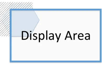
For the latter, a good example is a hardware renderer that allows rendering polygons. The user might want to just render a portion of that polygon somewhere in a corner of the screen as shown in Figure 6. In such a case, the user simply asks the hardware renderer to render the polygon with negative X and Y coordinates. The renderer itself doesn’t implement any clipping (this will be discussed shortly) so the renderer simply renders the entire polygon and the framebuffer interface will throw out any write transactions outside of the framebuffer area.
Display Area
Page 17 of 39
12.5.2 Read
Disclaimer: Due to time restrictions, the read portion of the framebuffer interface could never be fully tested. While the design described in this section is final/complete the actual implementation will still need some work.
As mentioned in the introduction of this chapter there are certain cases where a renderer needs to be able to read-back the current contents of the framebuffer to perform its job. Therefore, a renderer needs a way to ask the framebuffer interface to issue a read transaction on the bus towards the framebuffer memory. In the simplest form, the renderer would simply assert a read request signal and wait for the data to be returned by the framebuffer interface. However, that would lead to synchronization issues. When a hardware renderer requires the contents of a portion of the framebuffer that is usually in order to modify that same portion (eg. By performing a scroll operation or by overlying a filter). This means that the renderer needs the most recent & up-to-date version of the framebuffer contents in respect of the rendering commands already issued by the user. The write FIFO of the framebuffer interface might still contain data that is relevant for the read-back operation that hasn’t been written to the actual framebuffer just yet. To prevent these sorts of problem, the read requests of a renderer are also being passed through the same FIFO as the write request. However, this means that the state machine that dispatches from the write FIFO needs to be able to distinguish between data-to-write and commands. This is achieved by adding an additional bit to the FIFO element width. This bit is from here on referred to as the D/C bit (Data/Command). The bit set to ‘1’ means that everything after that bit represents a command that needs to be interpreted by the framebuffer interface while the bit set to ‘0’ means that everything after that bit is the relative framebuffer address and the data to be written at that address.
At the moment, the only commands that the framebuffer interface can interpret is a read request and modifying the clipping area (explainer later on). In fact, there are two different read commands that can be issued: One is for linear reads and the other one is for window wrapper reads.
Data that was read back from the framebuffer by the framebuffer interface are stocked into the read FIFO from which the hardware renderers can dispatch. There are two benefits from having this FIFO:
• If a renderer would have to do some processing that prevents it from reading the data that was read back from the FBI immediately this would mean that the renderer would lock up the Avalon bus (the FBI would have to assert the waitrequest signal which would force the memory controller to hold on which would in turn potentially halt the entire system (other components such as the CPU couldn’t access the memory either during that time). This FIFO allows the FBI to check whether there’s enough room to stock the data that it will request from the memory controller prior to actually issuing the read command.
• The FBI can make burst reads as multiple values can be stocked in the FIFO.
Note that the read FIFO is usually many times smaller than the write FIFO. This is due to the fact that a renderer that requested a pixel-readback will usually have to wait for that information before it can continue and therefore immediately dispatches the data from the FBI read FIFO.
Page 18 of 39 12.5.2.1 Linear read
With a linear read, the renderer simply provides the relative address of the first pixel value he wants to read back and a count in number of pixels. The framebuffer interface will not provide any wrapping but simply increment the address until the specified amount of pixels values have been read back. A linear read request consists of the following values being written to the FIFO in that order:
1. Read command (D/C bit set to ‘1’ and proper command constant (0x02)) 2. Start address of the first pixel that will be read back
3. Number of reads to be performed (in pixels) This is explained in more detail in section 12.5.5.2.
12.5.2.2 Rectangular read
In contrast to the linear read described above, the rectangular read allows a hardware renderer to specify a rectangular window inside the framebuffer. The framebuffer interface will take care of calculating the corresponding addresses and wrap at the edges of the rectangle. Basically, this allows a renderer to get a copy of the contents of a rectangular section of the framebuffer.
A rectangular read request consists of the following values being written to the FIFO in that order: 1. Read command (D/C bit set to ‘1’ and proper command constant (0x03))
2. Framebuffer address of the first pixel that will be read back 3. Width of the window (in pixels)
4. Height of the window (in pixels)
This is explained in more detail in section 12.5.5.3.
In both reading modes, the framebuffer interface uses the framebuffer base address to transform the relative addresses to absolute ones and uses the framebuffer span information to prevent reading from memory that isn’t part of the framebuffer. Note that the latter is a limitation that prevents off-screen area blitting – a scenario where for example the CPU decodes an image in RAM (but not the framebuffer) and then simply asks the hardware blitting engine (renderer) to copy the decoded image to the appropriate location(s) inside of the framebuffer.
12.5.3 Clipping
Clipping10 is a technique that allows to limit the area (in the framebuffer) that will be affected by a
rendering operation. At its most basic form (and with respect to operating only in two dimensions) clipping consists of a rectangular area with a given size and at a given position within the framebuffer. When rendering something only pixels inside that rectangular area get updated. All the pixels outside of the clipping area are unaffected by any rendering operations. More complex clipping engines allow defining clipping areas of arbitrary shapes. For example, this allows rendering only a circular area of a regular rectangular image.
Currently the clipping takes place in the framebuffer interface and only one clipping region is supported. Changing the clipping area happens by changing the clipping parameters in the corresponding registers through the CPU. The values of the clipping registers are being passed through
Page 19 of 39 the write FIFO as commands by the internal dispatcher. The reason for this is the same as for why read requests get passed through the write FIFO: The user might be changing the values of the clipping registers while some of the rendering operations are still in the write FIFO which would lead to unexpected results on the display. Passing everything through the same FIFO provides complete determinism as everything is being executed in chronological order.
Changing the clipping area position & size consists of the following values being written to the FIFO in that order:
1. Read command (D/C bit set to ‘1’ and proper command constant (0x01)) 2. X coordinate of the window (in pixels)
3. Y coordinate of the window (in pixels) 4. Width of the window (in pixels) 5. Height of the window (in pixels) This is explained in more detail in section 12.5.5.4.
12.5.4 Read and write FIFO
The various hardware renderers communicate with the framebuffer interface through the write- and the read-FIFOs. The formats of the data inside the FIFOs are complex as they combine multiple information into one FIFO element. For example, the write-FIFO contains the D/C bit and depending on that D/C bit the rest of the data is either a command value or the framebuffer address and data combined (concatenated). To simplify the life of a hardware renderer developer both FIFOs provide glue logic towards the hardware renderers to split-up and combine these signals to individual, more intuitive signals.
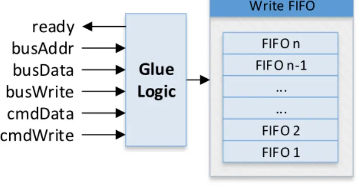
Figure 7 shows the write-FIFO with the corresponding glue logic in front of it:
FIFO n FIFO n-1 ... Write FIFO
Glue
Logic
ready
busAddr
busData
busWrite cmdDatacmdWrite
... FIFO 2 FIFO 1Figure 7: FBI write-FIFO glue logic
The ready signal indicates where the framebuffer interface is ready to receive new data or commands. This is the inverted isFull signal of the write-FIFO. A renderer must not issue new write transactions to the write-FIFO by strobing busWrite or cmdWrite if ready is logic ‘0’. Behavior is undefined in such a case.
A renderer can alter the framebuffer contents by assigning the relative framebuffer address of the pixel in question to busAddr and by setting busData to the corresponding pixel value (color value). A one clock cycle long strobe on busWrite will store that information as a “data package” in the write-FIFO in a format that the framebuffer interface behind the write-FIFO understands.
Page 20 of 39 A renderer can issue commands to the framebuffer interface (such as issuing a read request or changing the clipping mask) by setting cmdData to the corresponding command and by applying a write strobe on cmdWrite.
Similarly, the read FIFO is also interfaced by glue logic to simplify the life of a renderer developer:
FIFO n FIFO n-1 ... Read FIFO
Glue
Logic
readFifoDataAvailable
readFifoData
readFifoDataValid
readFifoReadAck
FIFO 2 FIFO 1Figure 8: FBI read-FIFO glue logic
The readFifoDataAvailable signal indicates that there is new data in the read-FIFO ready to be dispatched by the renderer. This is the inverted isFull signal of the read-FIFO.
The readFifoData is the actual data on the output port of the read-FIFO.
It can happen that the framebuffer interface can’t complete a requested read operation for example because the renderer requested reading from an invalid memory section. The readFifoDataValid signal indicates, whether the data is actually to be interpreted by the renderer as in such a case the framebuffer interface will just provide dummy data to complete the read request.
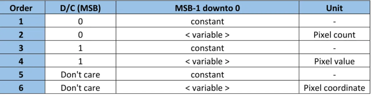
12.5.5 FIFO data format
The previous sections explained the historical development of the framebuffer interface and its capabilities. The following is a summary of the data that needs to be written into the write-FIFO of the framebuffer interface to perform the corresponding tasks.
The commands that need to be written into the write-FIFO of the framebuffer interface by a renderer are documented in tabular form:
Order D/C (MSB) MSB-1 downto 0 Unit
1 0 constant -
2 0 < variable > Pixel count
3 1 constant -
4 1 < variable > Pixel value
5 Don't care constant -
6 Don't care < variable > Pixel coordinate Table 3: Framebuffer interface write-FIFO data format synopsis
Parameters are being listed in ascending order from top to bottom. This means that the top most parameter is the first one to be written to the FIFO. The D/C (MSB) column specifies the state of the D/C bit. The MSB-1 downto 0 column the rest of the bits of the FIFO width. The values of the columns D/C (MSB) and the MSB-1 downto 0 will be concatenated (in that order, left-to-right) and written to the FIFO.
Page 21 of 39 Note that the number of bits for the data and the address are configured through the corresponding generics named dataBitNb and addrBitNb. From this, the write-FIFO size has been deduced as:
𝑤𝑟𝑖𝑡𝑒𝐹𝑖𝑓𝑜𝐵𝑖𝑡𝑁𝑏 = 𝑑𝑎𝑡𝑎𝐵𝑖𝑡𝑁𝑏 + 𝑎𝑑𝑑𝑟𝐵𝑖𝑡𝑁𝑏 + 1 The +1 is to take the D/C bit discussed earlier into account.
All framebuffer addresses are relative addresses where 0x00 is the first pixel in the framebuffer as the framebuffer interface will add the base address / offset of the framebuffer itself.
12.5.5.1 Write
Issuing a write transaction to the framebuffer is pretty straightforward and simple. As this will be by far the most used operation in the framebuffer interface it is crucial that it takes as little time as possible.
Order D/C (MSB) MSB-1 downto 0 Unit
1 0 <data> & <address> -
Table 4: Framebuffer interface write-FIFO data format for write transaction
Example: Writing the color value 0xAAAAAA to the address 0xBBBBBBBB assuming that both dataBitNb and addrBitNb are 32 requires writing the following into the write-FIFO:
Order D/C (MSB) MSB-1 downto 0 Unit
1 0 0x00AA AAAA BBBB BBBB -
Combined: 0x0 00AA AAAA BBBB BBBB
Table 5: Framebuffer interface write-FIFO data format for write transaction example
12.5.5.2 Linear read
Performing a linear read requires two parameters: The start address (address of the first pixel in the framebuffer) and the number of pixels to be read back:
Order D/C (MSB) MSB-1 downto 0 Unit
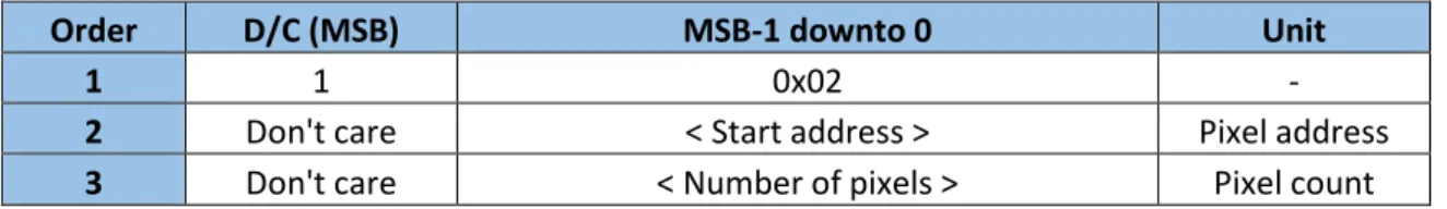
1 1 0x02 -
2 Don't care < Start address > Pixel address 3 Don't care < Number of pixels > Pixel count
Table 6: Framebuffer interface write-FIFO data format for linear read
Example: Reading back 13 pixels starting at the relative framebuffer address 0x3E7 assuming that both dataBitNb and addrBitNb are 32 requires writing the following into the write-FIFO:
Order D/C (MSB) MSB-1 downto 0 Unit
1 1 0x0000 0000 0000 0002 -
2 Don't care 0x0000 0000 0000 03E7 Pixel address 3 Don't care 0x0000 0000 0000 000D Pixel count
Page 22 of 39 12.5.5.3 Rectangular read
Performing a rectangular read requires three parameters: The start address (address of the first pixel in the framebuffer) and the width and height of the rectangular window:
Order D/C (MSB) MSB-1 downto 0 Unit
1 1 0x03 -
2 Don't care < Start address > Pixel address 3 Don't care < Rectangle width > Pixel count 4 Don't care < Rectangle height > Pixel count
Table 8: Framebuffer interface write-FIFO data format for rectangular read
Example: Reading back the pixels of a rectangle measuring 82 pixels in width and 64 pixels in height starting at the first pixel at address 0x3E7 assuming that both dataBitNb and addrBitNb are 32 requires writing the following into the write-FIFO:
Order D/C (MSB) MSB-1 downto 0 Unit
1 1 0x0000 0000 0000 0003 -
2 Don't care 0x0000 0000 0000 03E7 Pixel address 3 Don't care 0x0000 0000 0000 0052 Pixel count 4 Don't care 0x0000 0000 0000 0040 Pixel count
Table 9: Framebuffer interface write-FIFO data format for rectangular read example
12.5.5.4 Modifying clipping area
Changing the clipping area requires writing the corresponding command followed by the four parameters which are X and Y coordinates and width and height dimensions of the new rectangular clipping area. Note that as described above the size of the FIFO is determined by the address and data bus width. However, the clipping parameters will be resized to coordBitNb.
Order D/C (MSB) MSB-1 downto 0 Unit
1 1 0x01 -
2 Don't care < Clipping area X coordinate > Pixel coordinate 3 Don't care < Clipping area y coordinate > Pixel coordinate 4 Don't care < Clipping area width > Pixel count 5 Don't care < Clipping area height > Pixel count
Table 10: Framebuffer interface write-FIFO data format for clipping area modification
Example: Changing the clipping area to X = 5, Y = 15, Width = 680, Height = 480 assuming that both dataBitNb and addrBitNb are 32 requires writing the following into the write-FIFO:
Order D/C (MSB) MSB-1 downto 0 Unit
1 1 0x0000 0000 0000 0001 -
2 Don't care 0x0000 0000 0000 0005 Pixel coordinate 3 Don't care 0x0000 0000 0000 000F Pixel coordinate 4 Don't care 0x0000 0000 0000 02A8 Pixel count 5 Don't care 0x0000 0000 0000 01E0 Pixel count
Page 23 of 39
12.6 Renderers
The GPU contains an isolated hardware rendering for each rendering operation that the GPU offers. Note: In the future, it will also be possible to have multiple instances of the same hardware rendering inside the GPU which allows to handle multiple rendering operations of the same type simultaneously. For example: Having more than one block to hardware render filled rectangles means that multiple filled rectangles can be rendered in parallel.
This section of the document will explain the basic theory of operation of the existing renderers. To properly understand the different terms used it might be required to read the datasheet first.
12.6.1 Pixel
The pixel renderer consists of a simple finite state machine (FSM) that dispatches the required parameters from the command FIFO and then calculates the relative framebuffer offset to issue a write request to the framebuffer interface.
The relative framebuffer address is calculated by using the following equation: 𝐹𝐵 𝑎𝑑𝑑𝑟 = (𝑥 + 𝑓𝑏𝑊𝑖𝑑𝑡ℎ ∗ 𝑦) ∗ 𝑓𝑏𝐵𝑦𝑡𝑒𝑠𝑃𝑒𝑟𝑃𝑖𝑥𝑒𝑙 The FSM is shown in Figure 9:
Idle
Fetch Execute
start =
fetchDone =
Figure 9: Pixel renderer FSM
Fetching is done by a simple counter that is used to grab all three parameters (X, Y, color) from the command FIFO.
12.6.2 Filled rectangle
The filled rectangle renderer works the same way as the pixel renderer except that it contains two more counters which are used to count in X and Y direction until the width and height of the rectangle have been reached. The pixel address calculation reflects this by extending the equation of the pixel renderer with the two counter values countX and countY:
𝐹𝐵 𝑎𝑑𝑑𝑟 = (𝑥 + 𝑐𝑜𝑢𝑛𝑡𝑋 + 𝑓𝑏𝑊𝑖𝑑𝑡ℎ ∗ (𝑐𝑜𝑢𝑛𝑡𝑌 + 𝑦)) ∗ 𝑓𝑏𝐵𝑦𝑡𝑒𝑠𝑃𝑒𝑟𝑃𝑖𝑥𝑒𝑙 This calculation is performed for each pixel in the rectangle.
Page 24 of 39
12.6.3 Clipping
The clipping renderer functions a bit different to the pixel and the filled rectangle renderers as it doesn’t alter the framebuffer contents but issues a command to the framebuffer interface instead. The only job this clipping renderer does it dispatching the clipping mask parameters (X, Y, width and height) from the command FIFO and feeding them to the write-FIFO of the framebuffer interface. The finite state machine is simpler in this case as the fetching and the execution can be merged into the same state. The clipping renderer dispatches the first parameter and immediately pushes it to the framebuffer interface write-FIFO and therefore only adds one clock cycle of latency.
Idle
Fetch
start =
fetchDone =
Figure 10: Clipping renderer FSM
After discussing the theory of operation of the different hardware renderers it is time to look at the actual implementation.
13 Implementation
Section 12 explains the internal structure of the IP-core. This section of the document looks at the actual implementation in code. As mentioned in section 12, the overall design shown there doesn’t necessarily correspond to the design implementation. Entities and files have been named differently and sometimes parts that are shown individually in the design overview are simply embedded somewhere else. While this might sound like bad practice it’s to keep everything clean and simple. The overview given in section 12 has been structured to show the flow & handling of data in a way that is easy to grasp and understand. However, in code it’s sometimes often simpler to organize the structure slightly differently.
This section won’t go through every line of code but instead just list the important bits and pieces that are necessary to understand the overall theory of operation. Mainly this consists of explaining the different files & entities. The entity tables will not list the data/signal types and ranges but instead just give a description detailed enough to understand the purpose of the generic/signal. Further details can be gathered easily from reading the code.
Note that the generics and ports of all hardware renderers are exactly the same. They are not listed in this section as section 14 will describe everything required to write a new hardware renderer and therefore will also list the entity in great detail.
Page 25 of 39
13.1 Silizium.vhd
The silizium.vhd file contains the top-level entity of the Silizium IP-core. It doesn’t do anything except for forwarding everything to an entity named silizium_implementation. This technique is there to prevent having to re-generate the entire code of the SoC in the QSys tool every time something changes in the actual implementation: This way QSys knows the interface of the Silizium IP-Core which is the only important thing for it. All the other code we write will just be copy-pasted by the QSys tool upon code generation and therefore doesn’t requiring re-generating the entire SoC design which can take several minutes.
Generics:
Name Description
dataBitNb Internal data handling width. Will be used in the future. DO NOT CHANGE THIS.
coordBitNb The number of bits required to represent a coordinate in two's complement.
colorBitNb The number of bits required to represent a color value (internally). cmdFifoNumWordsExp The exponent of the size of the input command FIFO in elements.
Actual size will be 2^n of this value.
fbAddrBitNb The width of the address bus of the framebuffer interface. fbDataBitNb The width of the data bus of the framebuffer interface. fbBurstcountBitNb The number of bits required for the burstcount signal. fbBytesPerPixel The number of bytes per pixel.
fbWidth The width of the framebuffer in pixels. fbHeight The height of the framebuffer in pixels.
fbWriteFifoNumWordsExp The exponent of the size of the framebuffer write FIFO in elements. Actual size will be 2^n of this value.
fbReadFifoNumWordsExp The exponent of the size of the framebuffer read FIFO in elements. Actual size will be 2^n of this value.
Table 12: silizium.vhd generics Ports:
Name Direction Description
reset in Global clock input
clock in Global reset input
avalon_slave_address in
Avalon-MM slave interface avalon_slave_read in avalon_slave_readdata out avalon_slave_write in avalon_slave_writedata in avalon_slave_waitrequest out avalon_master_address out
Avalon-MM master interface avalon_master_write out
avalon_master_writedata out avalon_master_waitrequest in avalon_master_read out
Page 26 of 39 avalon_master_readdata in
avalon_master_readdatavalid in avalon_master_burstcount out
Table 13: silizium.vhd ports
13.2 Silizium_implementation.vhd
This file contains the actual top-level implementation of the Silizium IP-Core. The entity is exactly he same as the one listed for the silizium.vhd file as all generics and ports are just being forwarded. This file contains the implementation of the slave interface which means that it hosts all registers and also creates the instance of the command FIFO. Furthermore, the instances of the dispatcher and the framebuffer interface are also being created here.
Generics:
Name Description
dataBitNb Internal data handling width. Will be used in the future. DO NOT CHANGE THIS.
coordBitNb The number of bits required to represent a coordinate in two's complement.
colorBitNb The number of bits required to represent a color value (internally). cmdFifoNumWordsExp The exponent of the size of the input command FIFO in elements.
Actual size will be 2^n of this value.
fbAddrBitNb The width of the address bus of the framebuffer interface. fbDataBitNb The width of the data bus of the framebuffer interface. fbBurstcountBitNb The number of bits required for the burstcount signal. fbBytesPerPixel The number of bytes per pixel.
fbWidth The width of the framebuffer in pixels. fbHeight The height of the framebuffer in pixels.
fbWriteFifoNumWordsExp The exponent of the size of the framebuffer write FIFO in elements. Actual size will be 2^n of this value.
fbReadFifoNumWordsExp The exponent of the size of the framebuffer read FIFO in elements. Actual size will be 2^n of this value.
Page 27 of 39 Ports:
Name Direction Description
reset in Global clock input
clock in Global reset input
avalon_slave_address in
Avalon-MM slave interface avalon_slave_read in avalon_slave_readdata out avalon_slave_write in avalon_slave_writedata in avalon_slave_waitrequest out avalon_master_address out
Avalon-MM master interface avalon_master_write out avalon_master_writedata out avalon_master_waitrequest in avalon_master_read out avalon_master_readdata in avalon_master_readdatavalid in avalon_master_burstcount out
Table 15: silizium.vhd ports
13.3 Silizium_dispatcher.vhd
The dispatcher receives all signals of the command FIFO required for reading from it and takes care of selecting the proper hardware renderer to execute the job. Each hardware renderer will dispatch his parameters itself from the command FIFO as the dispatcher doesn’t know how many parameters each hardware renderer needs.
Generics:
Name Description
dataBitNb Internal data handling width. Will be used in the future. DO NOT CHANGE THIS.
coordBitNb The number of bits required to represent a coordinate in two's complement.
colorBitNb The number of bits required to represent a color value (internally). fbAddrBitNb The width of the address bus of the framebuffer interface.
fbDataBitNb The width of the data bus of the framebuffer interface. fbBytesPerPixel The number of bytes per pixel.
fbWidth The width of the framebuffer in pixels. fbHeight The height of the framebuffer in pixels.
Table 16: silizium_dispatcher.vhd generics Ports:
Name Direction Description
reset in Global clock input
Page 28 of 39 fifoEmpty in isEmpty signal of the command FIFO
fifoRdAck out Read acknowledge signal of the command FIFO fifoData in Data output port of the command FIFO
enable in Dispatcher enable input
busy out Dispatcher isBusy output
fbiBusAddr out FBI write-pixel address bus fbiBusData out FBI write-pixel data bus fbiBusWrite out FBI write-pixel write strobe fbiCmdData out FBI command data bus fbiCmdWrite out FBI command write strobe fbiIsReady in FBI isReady signal
fbiReadFifoDataAvailable out FBI read-FIFO newDataAvailable signal fbiReadFifoData out FBI read-FIFO data output port
fbiReadFifoDataValid out Whether the fbiReadFifoData data is valid fbiReadFifoReadAck in Read acknowledge signal of the FBI read FIFO
Table 17: silizium_dispatcher.vhd ports
13.4 Silizium_framebufferinterface.vhd
The framebuffer interface implemented in this file dispatches maintains the write-FIFO and read-FIFO and talks to the actual framebuffer memory over the corresponding Avalon-MM master interface. Generics:
Name Description
coordBitNb The number of bits required to represent a coordinate in two's complement.
addrBitNb The width of the address bus of the framebuffer interface. dataBitNb The width of the data bus of the framebuffer interface. burstcountBitNb The number of bits required for the burstcount signal. bytesPerPixel The number of bytes per pixel.
writeFifoNumWordsExp The exponent of the size of the framebuffer write FIFO in elements. Actual size will be 2^n of this value.
readFifoNumWordsExp The exponent of the size of the framebuffer read FIFO in elements. Actual size will be 2^n of this value.
Page 29 of 39 Ports:
Name Direction Description
reset in Global clock input
clock in Global reset input
enable in Enable/disable the framebuffer interface activities boundaryChecksEnable in Enable/disable the memory boundary checks clippingEnable in Enable/disable the rectangular clipping mask avalon_master_address buffer
Avalon-MM master interface avalon_master_write out avalon_master_writedata out avalon_master_waitrequest in avalon_master_read out avalon_master_readdata in avalon_master_readdatavalid in avalon_master_burstcount out
fbAddrBase in Framebuffer memory base address
fbAddrSpan in Framebuffer memory section span in bytes busAddr in write-pixel address bus
busData in write-pixel data bus
busWrite in write-pixel write strobe
cmdData in command data bus
cmdWrite in command write strobe
ready out isReady signal (inverted writeFifoIsFull signal) readFifoDataAvailable out Whether new data is available to be read readFifoData out Read FIFO data output port
readFifoDataValid out Whether the data on readFifoData is valid (valid read) readFifoReadAck in Read acknowledge signal of the read FIFO
writeFifoUsedWords out Number of used words of the write FIFO writeFifoClear in Signal to clear the write FIFO
readFifoUsedWords out Number of used words of the read FIFO readFifoClear in Signal to clear the read FIFO
clipX out The X coordinate of the current clipping mask clipY out The Y coordinate of the current clipping mask clipWidth out The width of the current clipping mask clipHeight out The height of the current clipping mask
Table 19: silizium_framebufferinterface.vhd generics
The internal design of the Silizium-IP core has been designed to allow for easy adding of new hardware renderers. The following section provides all the information necessary to implement new hardware renderers.
Page 30 of 39
14 Adding new renderers
This section explains everything required to implement a new hardware renderer into the existing infrastructure of the Silizium IP-Core.
A hardware renderer must have an entity that matches the ports listed in Table 21. Table 20 lists all generics that are available to a hardware renderer.
14.1 Generics
Table 20 lists the generics with type information, default values and the corresponding descriptions:
Name Type Default Description
dataBitNb positive 32 The width of the command FIFO.
coordBitNb positive 32 The number of bits required to represent a coordinate in two's complement.
colorBitNb positive 32 The number of bits required to represent a color value. cmdFifoNumWordsExp positive 7 The exponent of the size of the input command FIFO in
elements. Actual size will be 2^n of this value. fbAddrBitNb positive 32 The width of the address bus of the framebuffer
interface.
fbDataBitNb positive 32 The width of the data bus of the framebuffer interface. fbBytesPerPixel positive 4 The number of bytes per pixel.
fbWidth positive 800 The width of the framebuffer in pixels. fbHeight positive 480 The height of the framebuffer in pixels.
Table 20: Silizium renderers interface generics
14.2 Ports
A hardware renderer must implement the port interface shown in Table 21:
Name Direction Type Range
reset in std_logic -
clock in std_logic -
start in std_logic -
dataInReady in std_logic -
dataIn in std_logic_vector dataBitNb-1 downto 0
readAck out std_logic -
busy out std_logic -
fbiBusAddr out unsigned fbAddrBitNb-1 downto 0 fbiBusData out std_logic_vector fbDataBitNb-1 downto 0
fbiBusWrite out std_logic -
fbiCmdData out std_logic_vector fbAddrBitNb+fbDataBitNb-1 downto 0
fbiCmdWrite out std_logic -
fbiIsReady in std_logic -
Page 31 of 39 Detailed explanation of each signal:
reset: Global reset input. clock: Global clock input.
start: This signal will be set to ‘1’ for one clock cycle by the dispatcher once the renderer is supposed
to start the rendering job. The current data element of the command FIFO is guaranteed to be the first parameter for the renderer.
dataInReady: This signal is set to ‘1’ if there is data to be dispatched in the command FIFO. The
renderer must not attempt to read from the command FIFO if this signal is not ‘1’. This signal is the inverted isEmpty signal of the command FIFO.
readAck: The renderer must assert this signal (setting it to ‘1’ for the duration of one clock cycle) once
a data element has been read from the FIFO.
busy: This active-high signal allows the dispatcher to check whether the renderer is still busy or not.
The renderer must set this signal to ‘1’ one clock cycle after the start strobe has been issued by the dispatcher. If this signal is not being driven ‘1’ by the renderer within that time frame the dispatcher assumes that the renderer finished and will start dispatching the next command from the command FIFO which will result in framebuffer corruption as the order of commands in the command FIFO has been mixed up (because the renderer didn’t get a change to dispatch the parameters from the FIFO).
fbiBusAddr: The renderer puts the framebuffer address of a pixel it wants to change on this signal. fbiDataAddr: The renderer puts the pixel value (color value) of a pixel it wants to change on this signal. fbiBusWrite: Asserting this signal causes the glue logic of the framebuffer interface to take the address
and data provided through fbiBusAddr and fbiDataAddr and putting them into the write-FIFO of the framebuffer interface. Therefore, asserting this signal will result in a change of the framebuffer memory (provided that the address passes the boundary checks (if enabled) and is inside the clipping mask (if enabled).
fbiCmdData: This signal is used to pass a command to the framebuffer interface. The available
commands are documented in section 12.5.1.
fbiCmdWrite: Asserting this signal causes the glue logic of the framebuffer interface to take the
command provided through fbiCmdData and putting it into the write-FIFO of the framebuffer interface.
fbiIsReady: This signal is provided by the framebuffer interface. The renderer must not assert
fbiBusWrite or fbiCmdWrite if this signal is not ‘1’. Behavior in such a case is undefined. This signal is the inverted isFull signal of the framebuffer interface write-FIFO. Therefore, fbiIsReady = ‘0’ indicates that the write-FIFO is full.
14.3 Infrastructure
Once a new renderer has been written it needs to be added into the existing Silizium infrastructure. This is done by creating an instance of the renderer in the dispatcher found in the file silizium_dispatcher.vhd. That file also contains the implementation of the demux and mux to select the appropriate renderer to which the new renderer needs to be hooked up. That process is