HAL Id: hal-02129304
https://hal.archives-ouvertes.fr/hal-02129304
Submitted on 14 May 2019
HAL is a multi-disciplinary open access
archive for the deposit and dissemination of
sci-entific research documents, whether they are
pub-lished or not. The documents may come from
teaching and research institutions in France or
abroad, or from public or private research centers.
L’archive ouverte pluridisciplinaire HAL, est
destinée au dépôt et à la diffusion de documents
scientifiques de niveau recherche, publiés ou non,
émanant des établissements d’enseignement et de
recherche français ou étrangers, des laboratoires
publics ou privés.
Temperature-induced transport changes in molecular
junctions based on a spin crossover complex
Lorenzo Poggini, Mathieu Gonidec, Ram Kumar Canjeevaram
Balasubramanyam, Lorenzo Squillantini, Gilles Pecastaings, Andrea Caneschi,
Patrick Rosa
To cite this version:
Lorenzo Poggini, Mathieu Gonidec, Ram Kumar Canjeevaram Balasubramanyam, Lorenzo
Squillan-tini, Gilles Pecastaings, et al.. Temperature-induced transport changes in molecular junctions based
on a spin crossover complex. Journal of Materials Chemistry C, Royal Society of Chemistry, 2019, 7
(18), pp.5343-5347. �10.1039/C8TC06587J�. �hal-02129304�
DOI: 10.1039/C8TC06587J1
www.rsc.org/
Temperature-induced transport changes in molecular junctions
based on a Spin Crossover complex
Lorenzo Poggini,*ab Mathieu Gonidec,*ab Ram Kumar C.B.,ab Lorenzo Squillantini,abc Gilles
Pecastaings,d Andrea Caneschic and Patrick Rosaab
This work describes the study of molecular junctions embedding the spin crossover complex [Fe(H2B(pz)2)2(phen)] as an active switchable thin film. In those junctions we observed that the spin state conversion causes a gradual increase in the current density, may be due to a crossover from direct tunneling to multi-step hopping.
Molecular-based materials start to catch the attention of the research community as a potential alternative to conventional inorganic semi-conductor materials, due to the possibility to incorporate them in advanced materials that can be easily processed, that are lightweight, and that can be incorporated in flexible devices. Switchable materials, i.e. materials able to reversibly switch their physical properties upon application of external stimuli (temperature, light-irradiation, applied magnetic and electric fields, pressure, etc.) are of relevant importance in material science for their potential technological applications as active material in functional devices.1–7 Among them, spin crossover (SCO)
complexes, in which the spin state of a metal ion can be switched between two distinct magnetic states (low-spin, LS, and high-spin, HS), are particularly appealing molecular materials for the preparation of molecular switches with reversible magnetic and electrical response.5
Only few studies have been reported so far on the integration of SCO materials in electrical and electromechanical devices,5,8 but one of the main challenges has resided in the
difficulties of obtaining high-quality thin films. Due to those drastic limitations, and notably to the difficulty to prepare non-short-circuited, high-quality devices, most of the studies to date have focused on rather thick films that operate in the hopping regime.
We believe, however, that there are very interesting phenomena to study on ultra-thin films (i.e. films which are at most a few nm thick) for which the tunnelling regime is usually expected be preponderant.9 Most interestingly, unlike hopping,
tunnelling characteristics should be temperature independent and would thus provide a flat baseline for SCO-induced current switching. Beyond simple electronic effects, interfacial
phenomena are extremely relevant for spintronics, and in this context it is important to increase our knowledge of molecular-scale phenomena instead of bulk behaviours.10
In a previous work7 we studied the tunnelling properties of
vertical junctions incorporating very thin films of a SCO complex, [Fe(HB(trz)3)2] (HB(trz)3 =
tris(1H-1,2,4-triazol-1-yl)borohydride), presenting a remarkably abrupt spin crossover slightly above room temperature. We had selected this compound as an experimentally easy accessible starting point, as it only required the capability to alter the temperature of the sample in a narrow range above room temperature. In those experiments, we showed that the temperature-induced spin transition of the compound translated in a major change in the current density flowing through AuTS//[Fe(HB(trz)3)2]//EGaIn
junctions. We observed an increase in log |J| of two orders of magnitude upon converting from the LS to the HS state, which we rationalized by a theoretical approach.7
These interesting results gave a first sight at the promising direct coupling between temperature-induced SCO and tunnelling in ultra-thin films. Nevertheless, this is still a budding field and much more experimental data are needed to fully understand it. In particular, our previous experiments were performed above room temperature (and thus above the freezing point of the EGaIn electrode) with thin films exhibiting a very abrupt SCO behaviour but complicated properties depending on the hydration state of the films.11,12 Since most
compounds exhibit SCO below room temperature, we believe that it is therefore important to study model high-quality SCO-junctions operating below room temperature, and more important below the freezing point of the liquid EGaIn top electrode.
a.CNRS, ICMCB, UMR 5026, F-33600 Pessac, France
b.Univ. Bordeaux, ICMCB, UMR 5026, F-33600 Pessac, France
c.DIEF - Department Industrial Engineering and INSTM Research Unit, University of
Florence, Via S. Marta 3, I-50139 Florence, Italy.
d.LCPO, CNRS UMR 5629, Université de Bordeaux, Bordeaux-INP, Pessac 33607
Cedex, France
E-mail: mathieu.gonidec@icmcb.cnrs.fr; lorenzo.poggini@icmcb.cnrs.fr
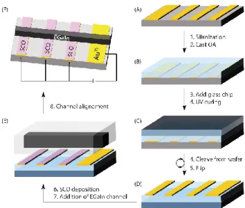
Figure 1. Fabrication of SCO-based tunneling junctions for temperature-dependent
measurements based on the design of Nijhuis et al.13 (A) We patterned
template-stripped gold (AuTS) stripes as the bottom electrodes by thermal evaporation of gold on
an ultra-flat silicon wafer through a shadow mask. To allow for an easy pealing of the stripes, we modified the SiOx, selectively, by vapour silanization with a fluorosilane. We cast a UV-curable optical adhesive (OA) to glue the MTS stripes to a glass chip, and after
UV exposure (C) we cleaved the Au/adhesive/glass composite from the wafer to obtain the array of electrodes (D). After thermal evaporation of 1 over the substrate, we filled a PDMS microchannel with EGaIn and brought it in contact with the array (E) to complete the junctions that could then be connected to the electrometer (F) and mounted inside a Linkam temperature control stage.
In this context, we have shown that the ferrous complex [Fe(H2B(pz)2)2(phen)] (pz = pyrazol-1-yl, phen =
1,10-phenanthroline) 1 is an ideal target, since it can be deposited as very smooth high-quality ultra-thin films by thermal evaporation while still maintaining its actuating properties.14
This is a very well-known compound for which the synthesis,15
structural characterizations,16 magnetic and photomagnetic
properties together with Raman and Mössbauer spectroscopies in bulk17–19 have been extensively described. We and others
elsewhere showed later on the feasibility of obtaining thin films by sublimation of 1 and reported their properties.14,20–23 In this
paper, we study the modulation in tunnelling current densities across AuTS//1//EGaIn junctions as a function of temperature
and film thickness. We show that, as expected, there is a significant change in current density with temperature due to the switching between HS and LS states. More precisely, we show that the system switches gradually from a low conductance state at low temperature (when the compound is in the LS state) to a high conductance state at high temperature (when the compound is in the HS state). We rationalize this behaviour by means of gas-phase DFT calculations. Interestingly, we detect no specific discontinuity around the freezing temperature of the EGaIn alloy, which could have modified the behaviour of the device due to the mechanical constraints on the SCO thin films, since SCO compounds are known to be sensitive to pressure.24
To measure molecular junctions incorporating 1 as the active switchable layer, we used as top electrode the eutectic alloy of indium and gallium (EGaIn), which acts as a soft, conformal, non-damaging top electrode as shown previously by
us and others.7,13,25,26 In order to study the junctions
characteristics at low temperature, we used arrays of crossbar geometries as described by Nijhuis et al.,13 in which the active
compound is evaporated on top of an array of template-stripped metal tracks, then covered with a top electrode
consisting in an open microchannel made of
polydimethylsiloxane (PDMS) filled with EGaIn (see Fig. 1). We then mounted the devices inside a Linkam stage equipped with electrical feedthrough connections to control the temperature while performing J-V measurements. We used this method to construct robust arrays of evaporated tunnel junctions and to study their J-V characteristics over a temperature range that was broad enough to encompass the complete thermal SCO temperature window (i.e. 100–300 K).
As it was already pointed out by Nijhuis et al.,13 it is critical
that the metal tracks be fully embedded in the optical adhesive to prevent short-circuits due to micro-fabrication defects at the edges of the template-stripped metal (Fig. 1). An important source of short-circuits in molecular junctions is the roughness of the metal films and the inhomogeneities and pinholes in the molecular film. However, template-stripping provides high-quality metal-films with a very low roughness, and it is well known that [Fe(H2B(pz)2)2(phen)] forms very smooth films down
to a few nanometres in thickness on gold.14 We checked the
quality of our evaporation process, and calibrated our tooling factor, by atomic force microscopy (AFM). We first evaporated a 20 nm thick film of compound 1 on an ultra-flat Si wafer through a porous mask, and we characterized the resulting film by AFM. As expected, the resulting film (see Figure S1) is very smooth, and we used those data to correct the experimental thicknesses by calibrating the equipment’s tooling factor, considering the error due to surface roughness. We then studied the morphology of a 10 nm thin film of 1 evaporated on a template-stripped gold substrate. On a 1×1 μm scale, the morphology of pristine AuTS (see Figure S2) and of a thin film of
1 (see Figure S3) were quite different, but both exhibited a very
low surface roughness (below 1 nm). The high quality of those films were also demonstrated by comparing their long range morphology to that of the ultraflat AuTS substrates: on a 20×20
μm scale both surfaces appear almost identical, without major defects or pinholes (see Figure S4).
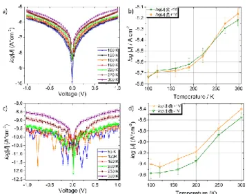
We prepared thin films of 1 of different thicknesses by thermal evaporation over template-stripped gold substrates. After taking into account the correction due to the tooling factor, the films we prepared had nominal thicknesses of 5.6±0.4, 11.2±0.8 and 16.7±1.1 nm. We performed temperature-dependent measurements from 100 to 300 K on the 5.6 and 16.7 nm films, and we collected a more extensive amount of room-temperature data on the 11.2 nm film by using a standard conical-tip methodology.
The 11.2 nm film (35 junctions, 350 traces, on a single film) presented log|J| values of -6.50 ± 0.09 and -6.39 ± 0.08 at +1.0 and -1.0 V, respectively (see Figure S5). The standard deviations of those measurements were smaller than that of similar measurements performed on AuTS//[Fe(HB(trz)3)2]//EGaIn
junctions,7 and for other junctions embedding self-assembled
that we got 100% yield in working junctions. These unusually narrow standard deviations and the absence of shorted junctions are remarkable and can be seen as a confirmation of the high quality of the thermally evaporated film of 1 on AuTS.
On the contrary, attempts to perform measurements with [Fe(H2B(pz)2)2(bipy)] (bipy = 2,2'-bipyridine), a closely related
compound that is well known to form rough films that are not necessarily continuous,14 only yielded shorted junctions.
We then performed temperature dependent
measurements on the 5.6 and 16.7 nm films. Thanks to the relatively high geometrical contact area in the crossbar junctions (about 1000×50 µm2), we were able to measure very
low current densities (down to log |J|≈ -9.5) with a reasonable signal-to-noise ratio, which constitutes a significant improvement in respect to our previous study.7 For both film
thicknesses, we measured full J/V traces between -1 and +1 V at different temperatures between 300 and 100 K (corresponding to the temperatures in which the SCO complex is in either HS or LS states as determined by magnetometry and by X-Ray Absorption Spectroscopy, XAS, in previous works14,22,30,31). The
log|J|/V curves measured between +1 V and -1V present the usual symmetrical V-shaped characteristics of non-rectifying junctions (see Figure 2). In both cases, upon increasing the temperature, the current density increased, with overall changes in the logarithm of current density, Δlog |J| measured at ± 1V, of about 0.6 and 1 for the 5.6 and 16.7 nm samples, respectively. Due to the rather gradual SCO behaviour measured by XAS usually displayed in thin films of 1 as compared to the bulk, it is not surprising that the current density changes very gradually with temperature.22,30
The trend in current density as a function of temperature is not very different from what was previously observed for the same compound with evaporated junctions using Al and ITO electrodes and with a higher thickness (30 nm).4 Nevertheless
the shape of the current vs. T curve does not match directly that of the SCO curve measured on bulk and thick film samples by standard magnetometry,14 but seems to be in line with what
was found for a sub-monolayer coverage.22 The discrepancy
with bulk samples is perhaps not surprising, as it has been
shown that for the first layer on Au(111) single crystal, ca. 80% of the molecules do not undergo spin crossover, and that a portion of those surface bound [Fe(H2B(pz)2)2phen] decompose
into [Fe(H2B(pz)2)2] and free phen moieties.22 Considering the
thickness of our films, those interfacial species should constitute only a small fraction (around 4-12%) of the total amount of compound 1 present in the films. Remarkably, even at room temperature, the log |J| vs T curves (both at +1 V) do not seem to reach a saturation value, and it is offset significantly towards high temperatures when compared to bulk susceptibility measurements.
Those unexpected features could be related to non-anticipated behaviour of compound 1 in our junctions (stress induced by the top electrode, pinning of the spin state due to the interactions with the bottom substrate, electrostriction…) or could be due to a more complex phenomenon, such as a change of transport mechanism with temperature. In particular, the latter situation would be quite complex as it could involve the combined effect of the change in spin state and the change in thermal energy. To try to unravel those mechanistic aspects, we compared the current densities in the AuTS//1//EGaIn
junctions as a function of thickness. As shown on Figure 3, log |J| appears to vary linearly with the thickness of the molecular film at both positive and negative biases, and the J/V curves are shifted towards higher current densities with decreasing film thicknesses. This result could point at direct tunnelling as the dominating mechanism at room temperature, for which the thickness dependence is often written in a simplified manner as:
𝐽(𝑉) = 𝐽0(𝑉)𝑒−𝛽𝑑
where J0 (A*cm-2) is a constant that depends on many variables
of the system including the contact resistance, the nature of the interfaces between the molecular layer and the electrodes and the properties of the molecules, while is the tunneling decay coefficient that depends essentially on the properties of the molecules (e.g. the frontier orbital energies). Nevertheless, the decay coefficients , resulting from the fitted experimental data, are very small (of the order of 0.6 nm-1 as opposed to the
usual values of the order of 10 nm-1 for many compounds). This
suggests that if the mechanism truly was tunnelling, the barrier height (that results from the difference in energy between the work functions of the electrodes and the frontier molecular orbitals of the compound) would be extremely small. In fact this
value is more in line with values measured for molecular junctions exhibiting multi-step hopping.9
Figure 2. (a,c) Plot log |J| vs V at different temperatures and b,d) plot of log |J| at ±1V
reported as a function of T for junctions incorporating 5.6 nm (a,b) and 16.7 nm (c,d) films of 1, respectively.
Figure 3. a) Plots of log |J| vs. V at room temperature for junctions of 1 with different
film thickness, and b) thickness dependence of the log |J| values at ± 1V. The continuous lines are the best linear fits to the data.
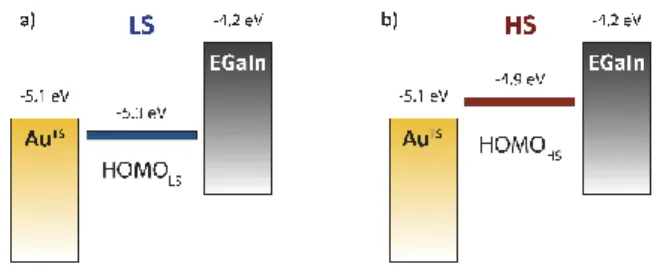
To shed some light on the small value, we performed gas phase DFT calculations (see details in the SI), to estimate the frontier orbital energies of compound 1 in both HS and LS states. The gas-phase calculations are of course an oversimplification of the system that does not take into account the interactions with the surface and between neighbouring molecules, but we have found, with other compounds and as pointed out in our previous study,7 that they provide a
reasonable ground to discuss the electronic configuration of our junctions. As it is often the case with molecular systems, the LUMOs lie very far from the work functions of the electrodes (we take φAu = 5.1 eV and φEGaIn = 4.2 eV) for both HS and LS
states, and hole transport should dominate the behaviour of the junctions. The relevant frontier orbitals are therefore the HOMOs with estimated orbital energies of about 5.3 eV and -4.9 eV for HS and LS, respectively. With those data, we constructed the molecular orbital diagram shown on Figure 4.
Figure 4. Electronic configuration of the junctions in open circuit for both HS (a) and LS
(b) states, respectively.
Based on this diagram, the HOMO energy in the LS configuration should be quite close to the fermi energy of the gold electrode but should still lie below the fermi energies of both top and bottom electrodes. It follows that direct hole tunnelling is likely to be the dominating transport mechanism below the T1/2 of
compound 1 (i.e. below ca. 150 K). For the HS state, however, the HOMO energy (-4.9 eV) lies between the Fermi energies of the top and bottom electrodes (-5.1 and -4.2 eV, respectively) while staying rather close to the work function of gold. This could support that, upon SCO, the system could exhibit a crossover from direct tunnelling to multi-step hopping.9,32 We
note that the energy difference between φAu and the HOMO
energy of compound 1 is rather small in both cases (0.2 eV for both HS and LS) and one should therefore be very cautious when assigning the precise nature of the transport mechanisms involved in those junctions. Nevertheless, such a crossover from a temperature-independent tunnelling regime to a thermally-activated one would account well for the relatively stable current densities we observed below 150 K, and the absence of saturation of the tunnelling current density even at room temperature.
Conclusions
In conclusion, we have studied ultra-thin molecular junctions incorporating high-quality films of the [Fe(H2B(pz)2)2(phen)]
spin-crossover complex and shown that such junctions present a significant variation in current density by temperature. To
perform this study, we used EGaIn-based crossbar tunnel junctions, a non-damaging technique that we recently employed to study another SCO based tunnel junction presenting a very abrupt current switching.7 In particular, we
wanted to check in this study whether junctions embedding compound 1 (that switches spin states about 160 K) would not be quenched by the freezing of the liquid metal top electrode (at 288 K). Instead, we show that the resulting AuTS//1//EGaIn
junctions present a change in current density of up to one order of magnitude with temperature. This change occurred in a very broad range of temperature (100-300 K), which is in line with what would be expected for SCO complexes exhibiting a gradual conversion, as was shown for ultrathin films of complex 1. This is a very important result as it shows that despite being below the freezing point of EGaIn, the device still presents spin-state switching that translates in a significant change in current density.
Thanks to DFT calculations, we can propose a rationalization of the behaviour of the devices and it seems as though the spin conversion is accompanied by a crossover from direct tunneling to a temperature activated multi-step hopping regime. Such crossovers are well known in oligo-aromatic molecular wires when varying the length of the compound.9,32 In the present
case, however, the switchable nature of the SCO complexes seems to allow to induce it in a single system by a change of temperature. This result, if confirmed, would open the door to interesting molecular switches in which the compounds could be engineered to favour such an inter-mechanism crossing, and that could be triggered by light irradiation thanks to the LIESST effect.
Conflicts of interest
There are no conflicts to declare.
Acknowledgements
This work was supported by the French National Research Agency (ANR) Investment for the Future Programme IdEx Bordeaux (ANR-10-IDEX-03-02) and the MOLSPIN COST action CA15128. Computer time for this study was provided by the computing facilities MCIA (Mésocentre de Calcul Intensif Aquitain) of the Université de Bordeaux and of the Université de Pau et des Pays de l'Adour. We also acknowledge the LCPO laboratory and all the ICMCB staff for their support with the measurements.
References
1 C. Bartual-Murgui, A. Akou, C. Thibault, G. Molnár, C. Vieu, L. Salmon and A. Bousseksou, J. Mater. Chem. C, 2015, 3, 1277–1285.
2 J. Linares, E. Codjovi and Y. Garcia, Sensors, 2012, 12, 4479–4492.
3 E. Ruiz, Phys. Chem. Chem. Phys., 2014, 16, 14–22. 4 C. Lefter, S. Rat, J. S. Costa, M. D. Manrique-Juárez, C. M.
Quintero, L. Salmon, I. Séguy, T. Leichle, L. Nicu, P. Demont, A. Rotaru, G. Molnár and A. Bousseksou, Adv. Mater., 2016, 7508–7514.
5 G. Molnár, S. Rat, L. Salmon, W. Nicolazzi and A. Bousseksou, Adv. Mater., 2018, 30, 1703862.
6 K. Senthil Kumar and M. Ruben, Coord. Chem. Rev., 2017,
346, 176–205.
7 L. Poggini, M. Gonidec, J. H. González-Estefan, G. Pecastaings, B. Gobaut and P. Rosa, Adv. Electron. Mater., 2018, 1800204, 1800204.
8 C. Lefter, V. Davesne, L. Salmon, G. Molnár, P. Demont, A. Rotaru and A. Bousseksou, Magnetochemistry, 2016, 2, 18. 9 L. Luo, S. H. Choi and C. D. Frisbie, Chem. Mater., 2011, 23,
631–645.
10 M. Cinchetti, V. A. Dediu and L. E. Hueso, Nat. Mater., 2017, 16, 507–515.
11 V. Shalabaeva, S. Rat, M. D. Manrique-Juarez, A.-C. Bas, L. Vendier, L. Salmon, G. Molnár and A. Bousseksou, J. Mater.
Chem. C, 2017, 5, 4419–4425.
12 S. Rat, K. Ridier, L. Vendier, G. Molnár, L. Salmon and A. Bousseksou, CrystEngComm, 2017, 19, 3271–3280. 13 C. A. Nijhuis, W. F. Reus, J. R. Barber, M. D. Dickey and G.
M. Whitesides, Nano Lett., 2010, 10, 3611–3619. 14 T. Palamarciuc, J. C. Oberg, F. El Hallak, C. F. Hirjibehedin,
M. Serri, S. Heutz, J.-F. Létard and P. Rosa, J. Mater. Chem., 2012, 22, 9690–9695.
15 J. A. Real, M. C. Muñoz, J. Faus and X. Solans, Inorg. Chem., 1997, 36, 3008–3013.
16 A. L. Thompson, A. E. Goeta, J. A. Real, A. Galet and M. Carmen Muñoz, Chem. Commun., 2004, 1390–1391. 17 N. Moliner, L. Salmon, L. Capes, M. C. Muñoz, J.-F. Létard,
A. Bousseksou, J. Tuchagues, J. J. McGarvey, A. C. Dennis, M. Castro, R. Burriel and J. A. Real, J. Phys. Chem. B, 2002,
106, 4276–4283.
18 A. Galet, A. B. Gaspar, G. Agusti, M. C. Muñoz, G. Levchenko and J. A. Real, Eur. J. Inorg. Chem., 2006, 2, 3571–3573.
19 S. Rat, M. Mikolasek, J. S. Costá, A. I. Chumakov, W. Nicolazzi, G. Molnár, L. Salmon and A. Bousseksou, Chem.
Phys. Lett., 2016, 653, 131–136.
20 H. Naggert, A. Bannwarth, S. Chemnitz, T. von Hofe, E. Quandt and F. Tuczek, Dalt. Trans., 2011, 40, 6364. 21 T. G. Gopakumar, F. Matino, H. Naggert, A. Bannwarth, F.
Tuczek and R. Berndt, Angew. Chemie - Int. Ed., 2012, 51, 6262–6266.
22 T. G. Gopakumar, M. Bernien, H. Naggert, F. Matino, C. F. Hermanns, A. Bannwarth, S. Mühlenberend, A. Krüger, D. Krüger, F. Nickel, W. Walter, R. Berndt, W. Kuch and F. Tuczek, Chem. - A Eur. J., 2013, 19, 15702–15709. 23 E. Ludwig, H. Naggert, M. Kalläne, S. Rohlf, E. Kröger, A.
Bannwarth, A. Quer, K. Rossnagel, L. Kipp and F. Tuczek,
Angew. Chemie - Int. Ed., 2014, 53, 3019–3023.
24 E. Tailleur, M. Marchivie, J.-P. Itié, P. Rosa, N. Daro and P. Guionneau, Chem. - A Eur. J., 2018, 24, 14495–14499. 25 R. C. Chiechi, E. A. Weiss, M. D. Dickey and G. M.
Whitesides, Angew. Chemie - Int. Ed., 2008, 47, 142–144. 26 L. Cademartiri, M. M. Thuo, C. A. Nijhuis, W. F. Reus, S.
Tricard, J. R. Barber, R. N. S. Sodhi, P. Brodersen, C. Kim, R.
C. Chiechi and G. M. Whitesides, J. Phys. Chem. C, 2012,
116, 10848–10860.
27 C. M. Bowers, K. Liao, H. J. Yoon, D. Rappoport, M. Baghbanzadeh, F. C. Simeone and G. M. Whitesides, Nano
Lett., 2014, 14, 3521–3526.
28 C. a. Nijhuis, W. F. Reus, J. R. Barber and G. M. Whitesides,
J. Phys. Chem. C, 2012, 116, 14139–14150.
29 M. Baghbanzadeh, F. C. Simeone, C. M. Bowers, K.-C. Liao, M. Thuo, M. Baghbanzadeh, M. S. Miller, T. B. Carmichael and G. M. Whitesides, J. Am. Chem. Soc., 2014, 136, 16919–16925.
30 S. Ossinger, H. Naggert, L. Kipgen, T. Jasper-Toennies, A. Rai, J. Rudnik, F. Nickel, L. M. Arruda, M. Bernien, W. Kuch, R. Berndt and F. Tuczek, J. Phys. Chem. C, 2017, 121, 1210– 1219.
31 M. Bernien, H. Naggert, L. M. Arruda, L. Kipgen, F. Nickel, J. Miguel, C. F. Hermanns, A. Krüger, D. Krüger, E. Schierle, E. Weschke, F. Tuczek and W. Kuch, ACS Nano, 2015, 9, 8960– 8966.
32 J. Vura-Weis, S. H. Abdelwahed, R. Shukla, R. Rathore, M. A. Ratner and M. R. Wasielewski, Science (80-. )., 2010,