Avant de rentrer dans le vif du sujet, je tiens à remercier toutes les personnes qui ont contribué de très près ou de plus loin à ce travail de thèse.
En premier lieu, je tiens à remercier Michel Haond pour m’avoir accueilli dans l’équipe "14FD" de STMicroelectronics, même si cette aventure n’aura duré qu’une petite année... Merci donc à Maud Vinet d’avoir bien voulu me récupérer au CEA-LETI dans son laboratoire LICL, sans quoi cette thèse n’aurait pas pu continuer dans de bonnes conditions. Merci à Franck Arnaud d’avoir pris le relais côté ST, d’avoir participé à ma soutenance et de m’intégrer dans son équipe pour la suite. Mes remerciements vont ensuite à mes co-encadrants François Andrieu et Didier Dutartre. Merci François pour ton encadrement de très grande qualité. J’ai eu la chance de bénéficier de tes compétences techniques et de ton état d’esprit remarquables. Tu as su me pousser grâce à ton enthousiasme et ton exigence. Merci d’avoir répondu à mes sollicitations permanentes tout en m’accordant une forte autonomie. C’était un réel plaisir d’être ton thésard. Merci Didier pour avoir toujours su porter de l’intérêt à mon travail, entre deux task forces... Ton expertise matériaux et ta pertinence m’ont épaté à de nombreuses reprises. Merci pour la confiance que tu m’as accordée. J’adresse également tous mes remerciements à mon directeur de thèse Alain Claverie. Merci Alain pour ton soutien à distance. Avec un peu de recul, je regrette de ne pas avoir assez "exploité" (je te cite) tes connaissances. Je te remercie également de t’être toujours préoccupé de mon bien-être en tant que thésard.
Je tiens ensuite à remercier tous les membres du jury d’avoir accepté d’évaluer cette thèse, en particulier les rapporteurs qui ont eu le courage de lire ce long manuscrit. Merci donc à Olivier Thomas (je ne suis pas prêt d’oublier la question sur l’effet des gradients de contrainte) et Sorin Cristoloveanu (merci de m’estimer au point de me faire participer à un reviewing). Merci également à Chantal Fontaine d’avoir présidé avec brio la soutenance et enfin à Damien Querlioz de s’être autant intéressé à mes travaux.
A STMicroelectronics, je tiens à remercier toutes les personnes qui étaient rattachées au programme "14FD". En particulier, je remercie Manu Josse pour ses coups de pouce et maitre Olivier Weber pour sa pédagogie à toute épreuve. Un grand merci à Pierre "pp41" Perreau pour la gestion des manips, à Raphaël Bingert pour l’initiation au SPICE ainsi que Pierre Morin pour nos discussions strain. Merci également à l’ensemble de l’équipe PI, en particulier Jérôme Mazurier, Elise Baylac, Manu Richard, Nelly Guillot, Sonar’, Manu Petitprez (merci de me former aujourd’hui), Claire Gallon, JC Grenier ... Je remercie également tous les autres intervenants sur le "14FD", notamment: Alexandre Pofelski, Marie-Anne Jaud, Thierry Poiroux, Fabien Rozé, Denis Rideau, Daniel Benoit, Victorien Paredes, Olivier Gourhant... Merci également à "Vince" Barral pour nos échanges sur l’ULPv2 ainsi qu’aux "fiabilistes" (i.e. l’équipe du SOC): coach Mus’, CD "minou", CND et Pat’. Enfin, merci mon co-box Nils pour ta maitrise d’IUI mais surtout pour les magnifiques photos que tu prends de moi. Au CEA-LETI, je remercie l’ensemble du LICL, laboratoire riche techniquement et humainement. Merci Cyrille Le Royer, Yves Morand, Christophe Plantier, garants de l’activité strain. Merci mes co-bureaux Valérie Lapras, une aventurière, et Olivier Rozeau (au revoir Madame). Merci Benoit "spin-up" Bertrand (vive LATEX!) et Louis "spin-down" Hutin, véritable Wikipedia ambulant (je ne fais que 95% confiance en la validité de tes facts, comme pour Wikipedia...). Merci Laurent "Lolo" Brunet pour la baseline, tes supers manips Coolcube et ta passion pour les trappeurs d’Alaska... Merci Perrine Batude de m’avoir confié la manip SDRASS et pour ton énergie débordante. Merci Bernard Previtali pour les caracs SEM, Claude Tabone pour son amour de la cantine et surtout Laurent Brevard, freerider de l’extrême qui m’a tant aidé sur le suivi des lots au LETI. Je remercie
Cooper (poor Gooner), Nicolas Bernier et Victor Boureau pour les mesures de strain. Merci Denis Rouchon pour notre étude µRaman. Merci Mikael "Mike" Cassé (tu resteras mon premier mentor) et Xavier "Zav" Garros (allez le PSEG!). Merci mon cher "piti": Alain Toffoli (vert de la première heure), Fabienne Allain (on se fait un double paramétrage sur Alisé) et Giovanni Romano ("cosi fan tutte"). Merci Frédérique Glowacki pour nos tentatives désespérées d’oxydation. Merci Shay Reboh pour nos discussions relaxation de SiGe et Comsol. Merci François Triozon pour les simulations NEGF et merci Benoit Matthieu pour nos comparaisons de simus méca. Merci Bastien Giraud, Reda Boumchedda et Jean-Philippe Noel pour les discussions SRAM. Je remercie également Joris Lacord, Jacques Cluzel (et son multimètre nommé "Revient"), Jean-Michel Hartmann, Vincent Mazzocchi, Pascal Besson, Pierrette Rivallin, Virginie Loup, ...
Je tiens également à remercier Joël Eymery, Vincent Favre-Nicollin et Gaëtan Girard pour les mesures à l’ESRF auxquelles j’ai eu la chance d’assister (je suis toujours curieux des résultats). Merci aussi à Gérard "GG" Ghibaudo pour m’avoir accordé du temps, même si je ne faisais pas partie de la horde de thésards qu’il dirige en parallèle.
J’adresse également mes remerciements à tous les thésards/stagiaires (aujourd’hui docteurs pour la plupart) pour tous les bons moments passés durant ces trois années. A ST, merci à la team du midi: Boris "Bob", BASTIEN, Giulio Uno, Giulio Due (je vous laisse débattre qui est qui), Romu "mais mec", Nils (un petit deuxième pour la route), Andrej, Carlos et enfin merci Hassan, ma petite feuille de vigne préférée, pour ta magnifique Megane tuning. Au Leti, un grand merci à la team Padawan du LICL: Alex ("voilà hein CuCube c’est fini"), Lina "Kadura-chan" pour le plus beau wallpaper ever, tes belles idées cadeau et surtout pour les chocobananas, Giulia "Pecorina" la teenager bisounours, Julien et tes talents d’imitateur, Carlos (hala Paris), Jessys (avec un s parce que tu es plusieurs), Loïc, Daphnée, Camila (don’t forget: Mathcad is fun, Mathcad is life), Mathilde, Sotiris (𝐸𝜐𝜒𝛼𝜌𝜄𝜎𝜏 𝜔)... Merci également à Gaspard pour une première expérience de co-encadrement de stage bien sympathique grâce à toi. Merci Blendissimo for your physics lessons and your stupid 50m-long shots. Pasa la pelota! Enfin, un grand merci à "Tonio" pour tous nos bons moments passés, du LCTE à Hawaii en passant par ton jardin avec cabanon. Bravo à toi pour ton triplé historique en cette saison 2017-2018 (job, bébé, doctorat). Café?
Pour finir, un grand MERCI à tous mes Martinérois. Merci la Fratrie pour fêter les week-ends avec le combo rituel "VnB + on mange où?" et merci pour les vannes inépuisables. Merci à mes beaux-parents Noun’ et Momo pour toute votre affection et à la belle-famille au sens large (mon beauf Nico, Agnès et Jean-Marc, Clé "poulet", Elsa, Soso, Mitmit’, Marine,...). Je remercie évidemment toute ma famille: Mamychèle (quel courage d’assister à cette ennuyante soutenance), PapyBajeat, TontonLuc, TontonPhi et ses angevins, etc... Je rajoute une tendre pensée pour PapyBernard et MamyJacqueline. Merci Papa, merci Maman, merci pour tout !!! Je termine ces remerciements avec les deux personnes qui me sont les plus chères: Merci Tom, mon petit frère modèle, véritable source d’inspiration quotidienne. Merci Lisa, ma crème de la crème, tout simplement indispensable. A nous le bonheur...
Introduction 7
1 Boosting sub-20nm CMOS technology performance: the relevance of strain 9
1.1 Introduction to CMOS logic . . . 10
1.1.1 The MOSFET, device at the heart of logic . . . 10
1.1.1.a The MOSFET switch . . . 10
1.1.1.b Boolean functions using logic combinatory gates . . . 11
1.1.2 The Power/Performance/Area metrics . . . 12
1.1.2.a Power/Performance: the ring-oscillator metrics . . . 12
1.1.2.b Area: standard cell design . . . 14
1.1.3 The MOSFET operation and metrics . . . 15
1.1.3.a The MOSFET structure . . . 15
1.1.3.b The MOSFET operation . . . 16
1.1.3.c The MOSFET principal metrics . . . 17
1.1.3.d The effective drive current in an inverter . . . 19
1.1.3.e The importance of the electrostatic control . . . 20
1.1.3.f The performance/leakage trade-off . . . 20
1.1.3.g The crucial role of carrier mobility . . . 21
1.2 CMOS technology scaling: the king is dead, long live the king ! . . . 24
1.2.1 The happy scaling, the good old days . . . 24
1.2.2 The introduction of goodies . . . 25
1.2.3 The rise of new architectures . . . 26
1.2.3.a The FinFET . . . 26
1.2.3.b The FDSOI technology . . . 27
1.2.3.c Stacked nanosheets . . . 29
1.2.4 The parasitics, key players . . . 30
1.2.5 CMOS scaling: conclusion and perspectives . . . 32
1.3 Strain integration in CMOS technologies . . . 34
1.3.1 Theory of elasticity . . . 34
1.3.2 The impact of strain on Silicon properties . . . 36
1.3.2.a Band structure of Silicon . . . 36
1.3.2.c Interaction with confinement . . . 40
1.3.2.d Summary . . . 41
1.3.3 Strain integration techniques . . . 42
1.3.3.a Locally-introduced strain techniques . . . 42
1.3.3.b Globally-introduced strain techniques . . . 44
1.3.4 Local Layout Effects . . . 47
1.3.5 Summary on strain integration in CMOS technology . . . 50
1.4 Conclusion to Chapter 1 . . . 50
2 Strained channel MOSFET performance: mobility and access resistance 51 2.1 Long channel mobility impacted by strain . . . 52
2.1.1 The split-CV technique . . . 52
2.1.2 Impact of strain on long channel mobility . . . 53
2.1.3 The piezoresistivity model . . . 54
2.2 Short channel mobility and access resistance extraction . . . 57
2.2.1 Total resistance method . . . 57
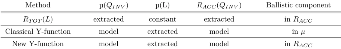
2.2.2 The Y-function methodology . . . 58
2.2.2.a Principle . . . 58
2.2.2.b Extraction procedure . . . 59
2.2.2.c Access resistance extraction . . . 62
2.2.3 Adapted Y-function with a new model of access resistance . . . 63
2.2.3.a Motivation: the role of the near spacer region . . . 63
2.2.3.b New Y-function-based method . . . 64
2.2.4 Summary . . . 66
2.3 The impact of strain on access resistance . . . 66
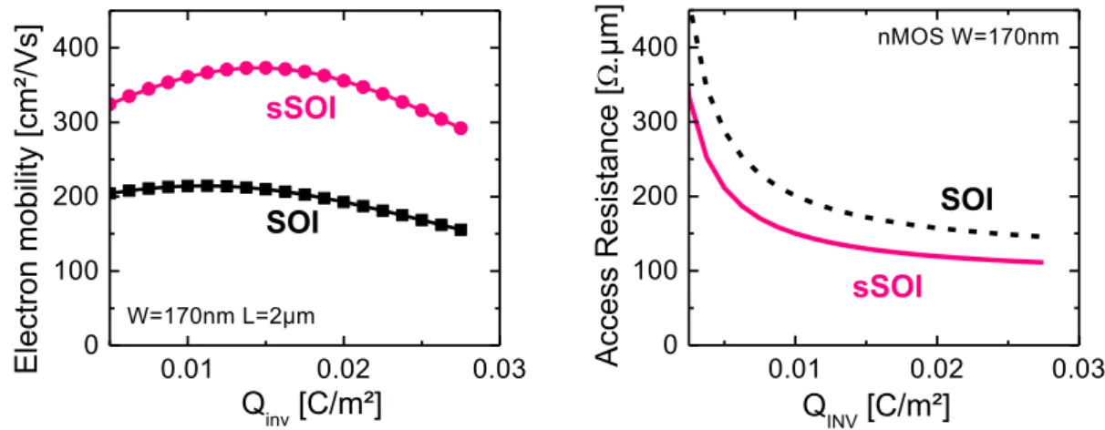
2.3.1 Planar FDSOI . . . 67
2.3.1.a Experimental results on sSOI . . . 67
2.3.1.b SiGeOI NEGF simulations . . . 68
2.3.2 Nanowires embedding strain . . . 69
2.3.3 Summary and SPICE predictions . . . 70
2.4 Conclusion to Chapter 2 . . . 72
3 Strain-induced layout effects in SiGeOI pMOSFETs 73 3.1 FDSOI technologies and devices . . . 74
3.1.1 28nm and 14nm FDSOI technologies at a glance . . . 74
3.1.2 Integration of SiGe in FDSOI . . . 76
3.1.2.a The condensation technique . . . 76
3.1.2.b SiGe integration in 14nm FDSOI technology . . . 79
3.2 Strain measurement, simulation and modeling in patterned SiGeOI . . . 81
3.2.2 Mechanical simulations . . . 84
3.2.2.a Hypotheses and model . . . 84
3.2.2.b Results and discussion . . . 85
3.2.3 Stress relaxation compact modeling . . . 86
3.2.3.a Theoretical approach: Hu’s model . . . 86
3.2.3.b Empirical approach: stress from SiGe channel . . . 87
3.2.4 µRaman measurements . . . 91
3.2.4.a Experimental details: samples and structures . . . 91
3.2.4.b Pseudomorphic SiGe strain extraction by µRaman . . . 92
3.2.4.c Unidirectional strain relaxation extraction by µRaman . . . 93
3.2.4.d Results . . . 94
3.2.4.e Conclusion on µRaman measurements . . . 98
3.2.5 Discussion . . . 99
3.3 Stress from SiGe source/drain: measurements, simulations and modeling . . . 100
3.3.1 Additional stress from SiGe source/drain in a non-patterned SiGeOI active layer 100 3.3.1.a NBED measurements and simulations . . . 100
3.3.1.b The influence of Germanium concentrations . . . 101
3.3.2 The impact of SiGeOI relaxation on stress from source/drain . . . 102
3.3.3 Stress from SiGe source/drain compact modeling . . . 103
3.4 Local Layout Effects: electrical results . . . 106
3.4.1 Electrical characteristics modeling . . . 106
3.4.2 28nm SiGeOI results . . . 107
3.4.2.a Impacts of orientation and Germanium concentration on performance . 107 3.4.2.b Local layout effects . . . 109
3.4.2.c Conclusion to 28nm results . . . 111
3.4.3 14nm SiGeOI results . . . 112
3.4.3.a Rectangular symmetrical and asymmetrical layouts . . . 112
3.4.3.b Non-rectangular layouts . . . 116
3.4.3.c Multifinger layouts . . . 118
3.4.3.d Active narrowing . . . 120
3.4.3.e Impact of Germanium concentration . . . 121
3.5 Conclusion to Chapter 3 . . . 124
4 Performance boosters for SiGeOI pMOSFETs 125 4.1 Introduction to chapter 4 . . . 126
4.2 Design solutions . . . 127
4.2.1 Intra-cell VT-mixing . . . 127
4.2.1.a Principle . . . 127
4.2.1.b SPICE simulation results . . . 127
4.2.2 The continuous-RX design . . . 133
4.2.2.a Principle . . . 133
4.2.2.b Isolation-gate construct . . . 133
4.2.2.c CRX performance evaluation . . . 135
4.2.2.d The impact of RX-jogs . . . 136
4.2.2.e The interest of a filler cell . . . 136
4.2.2.f Continuous-RX: summary . . . 137
4.2.3 Design solution benchmark . . . 138
4.2.4 SiGe introduction in FDSOI SRAM bitcells . . . 140
4.2.4.a Introduction . . . 140
4.2.4.b SiGe in classical SRAM . . . 141
4.2.4.c Complementary SRAM . . . 143
4.2.4.d Conclusion . . . 145
4.3 Technology solutions . . . 147
4.3.1 The SiGe-last approach . . . 147
4.3.1.a Process integration . . . 147
4.3.1.b Layout effects . . . 148
4.3.1.c Experimental performance . . . 151
4.3.1.d Discussion . . . 151
4.3.2 Dual Isolation by Trenches and Oxidation . . . 153
4.3.2.a Process integration . . . 153
4.3.2.b Device electrical results . . . 155
4.3.2.c Strain characterization . . . 158
4.3.2.d Performance . . . 160
4.3.2.e Back-biasing enabled by DITO . . . 161
4.4 Conclusion to Chapter 4 . . . 164
5 Next generation strained FDSOI CMOS devices 165 5.1 Tensile strain from strained-SOI substrate . . . 166
5.1.1 sSOI performance . . . 166
5.1.2 sSOI Local Layout Effects . . . 167
5.1.3 Conclusion . . . 170
5.2 The BOX-creep technique . . . 172
5.2.1 Introduction : the BOX-creep principle . . . 172
5.2.2 Mechanical simulations . . . 172
5.2.2.a Hypotheses and model . . . 172
5.2.2.b The BOX-creep mechanism . . . 174
5.2.2.c Impact of SiN parameters . . . 174
5.2.2.d The role of pad oxide and layout effect . . . 175
5.2.2.e Compatibility with SiGe channel . . . 176
5.2.3 Electrical results . . . 178
5.2.3.a BOX-creep with tensile LPCVD SiN . . . 178
5.2.3.b BOX-creep with compressive PECVD SiN . . . 180
5.2.4 Discussion and perspectives . . . 181
5.3 The SDRASS technique . . . 184
5.3.1 Introduction: the STRASS technique . . . 184
5.3.2 SDRASS principle and experiment details . . . 184
5.3.3 Morphological results . . . 185
5.3.4 Electrical results . . . 187
5.3.5 Conclusion and perspectives . . . 189
5.4 Dynamic Back-Bias in 3D-monolithic . . . 191
5.4.1 Introduction to 3D-monolithic . . . 191
5.4.2 Electrostatic coupling in 3D-monolithic . . . 192
5.4.2.a Experimental results . . . 192
5.4.2.b 3D 14nm Design-Kit . . . 193
5.4.3 Performance/Power . . . 194
5.4.3.a The role of back-gate extension . . . 194
5.4.3.b Layouts and environment . . . 194
5.4.4 6T-SRAM with local back-gate . . . 198
5.4.4.a Double-gate modes . . . 198
5.4.4.b Write-assist technique . . . 200
5.4.5 Conclusion . . . 201
General conclusion 203
Bibliography 207
Appendix 231
A Hu’s model of patterning-induced strain relaxation 231
B SRAM static testbench 233
C Résumé en français 239
Publications 265
Symbol Definition Unit
𝛼 Activity factor
-𝛾 Body factor V/V
𝛥𝜔𝑆𝑖𝑆𝑖 Si-Si Raman frequency peak shift m−1
𝜀 Strain
-𝜀0 Permittivity of vacuum F/m
𝜀𝑆𝑖 Permittivity of Silicon F/m
𝜂 Viscosity Pa.s
𝜃𝑖 Mobility attenuation parameters V−𝑖
𝜆 (Chap.2) Parameter of access resistance dependence with inversion charge Ω/V
𝜆 (Chap.3-5) Typical relaxation length m
𝜆0 Mean free path m
𝜇0 Low-field mobility m2/Vs
𝜇𝐵 Apparent ballistic mobility m2/Vs
𝜇𝑒𝑓 𝑓 Effective mobility m2/Vs
𝜈 Poisson’s ratio
-𝛯 Deformation potential eV
𝛱 Piezoresistive coefficient Pa−1
𝜎 Mechanical stress Pa
𝜎 (Chap.2) Parameter of access resistance dependence with inversion charge Ω.V
𝜏 Relaxation time s
𝜏𝑃 Propagation delay s
𝜑𝑓 Fermi potential eV
𝜑𝑀 Metal work function eV
𝜑𝑆 Semiconductor work function eV
𝜒𝑆 Electron affinity eV
𝜓𝑆 Surface potential eV
𝜔 RX-jog ratio
-𝜔0 Raman frequency peak of Silicon m−1
𝐶𝑑 Drain capacitance F
𝐶𝐸𝐹 𝐹 Effective capacitance F
𝐶𝑔 Gate capacitance F
𝐶𝑔𝑐 Gate-to-channel capacitance F
𝐶𝑖𝑗 Elastic constants Pa
CTE Coefficient of Thermal Expansion K−1
𝐸 Moung’s modulus Pa
𝐸// Longitudinal field V/m
𝐸𝐶 Conduction band energy eV
𝐸𝐷𝑃 Energy Delay Product J.s
𝐸𝑒𝑓 𝑓 Transverse effective field V/m
𝐸𝐺 Band gap energy eV
𝐸𝑂𝑇 Equivalent Oxide Thickness m
𝐸𝑉 Valence band energy eV
𝐹 𝑟𝑒𝑞, 𝑓 Frequency Hz
𝑔𝑚 Transconductance A/V
~ Reduced Planck constant J.s
𝐼𝐷𝐷𝑄 Leakage current (also called stand-by or static current) A
𝐼𝐷𝑌 𝑁 Dynamic current A
𝐼𝐸𝐹 𝐹 Effective drain current A (or µA/µm)
𝐼𝐿𝐼𝑁 Linear drain current A (or µA/µm)
𝐼𝑂𝐷𝐿𝐼𝑁 Linear drain current at a given gate overdrive A (or µA/µm)
𝐼𝑂𝐹 𝐹 OFF-state current or leakage current of a MOSFET A (or A/µm)
𝐼𝑂𝑁 ON-current or saturation current A (or µA/µm)
𝐼𝑡ℎ Drain current criterion for threshold voltage extraction A
𝑘, 𝑘𝐵 Boltzman constant J/K
k Wavevector
-L Transistor gate length m
𝑚* Effective mass kg
𝑚0 Longitudinal mass kg
𝑚𝑙 Transverse mass kg
𝑚𝑡 Rest mass of electron kg
𝑁𝐴 Acceptor impurities concentration A/cm3
𝑛𝑖 Intrinsic carriers concentration cm−3
𝑃𝐷𝑌 𝑁 Dyamic power W
𝑃𝑆𝑇 𝐴𝑇 Static power W
𝑃𝑇 𝑂𝑇 Total power W
𝑞 Elementary charge C
𝑅𝐸𝐹 𝐹 Effective resistance Ω (or Ω.µm)
𝑅𝑂𝑁, 𝑅𝑇 𝑂𝑇 ON-resistance in linear regime and at a given gate overdrive Ω or Ω/µm
𝑆𝑖𝑗 Stiffness constants Pa−1
SNM Static Noise Margin V
𝑆𝑆 Subthreshold swing mV/dec
𝑡𝑜𝑥 Gate oxide thickness m
VB Back-bias voltage (Body voltage) V
𝑣𝑑 Drift velocity m/s 𝑣𝑖𝑛𝑗 Injection velocity m/s 𝑣𝑠𝑎𝑡 Saturation velocity m/s 𝑣𝑇 Thermal velocity m/s VD Drain voltage V VDD Supply voltage V VFB Flat-band voltage V VG Gate voltage V VS Source voltage V VT Threshold voltage V
VTLIN Threshold voltage in linear regime V
VTSAT Threshold voltage in saturation regime V
W Transistor width m
WNM Write Noise Margin V
Acronym Definition
BEOL Back-End Of Line
BOX Buried OXide
CA Active contact layer
CB Gate contact layer
CESL Contact Etch Stop Layer
CMOS Complementary Metal Oxide Semiconductor CMP Chemical-Mechanical Planarization
CPP, CGP Contacted-Poly Pitch, Contacted Gate Pitch
CRX Continuous-RX
DTCO Design/Technology Co-Optimization EDX Energy-dispersive X-ray spectroscopy
FBB Forward Back-Bias
FDSOI Fully Depleted Silicon On Insulator FEOL Front-End Of Line
FWHM Full Width at Half Maximum
FO Fan-Out
GAA Gate-All-Around
GP Ground Plane
HH Heavy Holes
HVT High-VT
IoT Internet of Things
IV Inverter
LH Light Holes
LLE Local Layout Effects LOCOS LOCal Oxidation of Silicon
LPCVD Low-Pressure Chemical Vapor Deposition
LVT Low-VT
M1 First level of metal M1P First-level metal pitch MEOL Middle-End Of Line
MOSFET Metal Oxide Semiconductor Field Effect Transistor NBED, NBD Nano-Beam Electron Diffraction
NEGF Non-Equilibrium Green’s Function
nFET, nMOS n-type Metal Oxide Semiconductor Field Effect Transistor
PD Pull-Down
PECVD Plasma-Enhanced Chemical Vapor Deposition PED Precession-Electron-Diffraction
pFET, pMOS p-type Metal Oxide Semiconductor Field Effect Transistor
PG Pass-Gate
PPA Power/Performance/Area
PU Pull-Up
RBB Reverse Back-Bias
RCS Remote Coulomb Scattering RTO Rapid Thermal Oxidation
SA, SB Gate-to-STI distance from left, right, side SADP Self Aligned Double Patterning
SAIPS Self-Aligned In-Plane Stressor SCE Short Channel Effects
SDB Single-Diffusion Break
SDRASS Source and Drain from Recrystallization of Amorphized SiGe on SOI SiGeOI Silicon-Germanium On Insulator
SIT Sidewall Image Transfer
SLVT Super-Low-VT
SMT Stress Memorization Technique SOI Silicon On Insulator
SPER Solid Phase Epitaxial Regrowth
SPICE Simulation Program with Integrated Circuit Emphasis SRAM Static Random Access Memory
SRB Strain-Relaxed Buffer
SRS Surface Roughness Scattering
sSOI Strained-SOI
STI Shallow Trench Isolation
STRASS Strained Si by Top Recrystallization of Amorphized SiGe on SOI TEM Transmission Electron Microscopy
TU Tucked-Under
UTBB Ultra-Thin Body and Buried oxide XRD X-Ray Diffraction
Context
For the past 50 years, the semiconductor industry has known an exponential growth that has affected our everyday life. From the discovery of the transistor effect by W. Shockley, J. Bardeen and W. H. Brattain at the Bell Labs in 1947, the first microprocessor was manufactured by Intel in 1971, embedding around 2300 transistors (Intel 4004). Today, a microprocessor can count more than 7 billion transistors (22-core Xeon Broadwell-E5 from Intel) and the global semiconductor industry sales raised to $335.2 billion in 2015. Such a growth has been enabled by an aggressive scaling of the integrated circuit dimensions. This so-called "happy scaling" has lost its efficiency to keep reducing the power consumption. Innovations were required, especially during the last decade when physical barriers had to be pushed back. As a result, the technology complexity has increased and different ingredients have been implemented.
In this context, the introduction of new transistor architectures has been necessary to meet the requirements both in terms of density and performance. Especially, the Fully Depleted Silicon On Insulator (FDSOI) technology has appeared as an alternative to the FinFET to succeed the historical planar bulk technologies. FDSOI technology has several strengths such as a good electrostatic control, a low variability and a great back-biasing capability. In addition to the change of transistor architecture, the use of strain as a performance booster has been widely discussed and is today mandatory in advanced technology. The work of this thesis deals with the strain integration in Fully Depleted Silicon On Insulator technology in order to boost and optimize the performance.
Manuscript organization
The manuscript is organized as follows:
The first chapter details the context of this work. The basics of the Complementary Metal Oxide Semiconductor (CMOS) technology are presented. First, a focus is made on the principle of operation of the field effect transistor, which is the key element for digital computing. Then, the CMOS technology evolution through the well-known scaling is depicted. Finally, the interest of strain integration to boost the performance is discussed.
The second chapter focuses on the performance of strained devices. In particular, the impact of strain on carrier mobility is investigated. A dedicated attention is paid on the electrical characteriza-tion of short channel transistors, emphasizing the crucial role of the access resistance and its strain dependence.
The third chapter discusses the use of strained SiGe channel in FDSOI technology. After presenting the FDSOI technology, a focus is made on the strain measurement and modelling in patterned SiGe active areas. An extensive study of the strain-induced layout effects is finally presented.
The fourth chapter aims at providing solutions to boost the performance of scaled devices embedding strain. This chapter is splitted into two main parts: design- and technology-based solutions.
In the fifth and last chapter, new strain integration techniques in FDSOI technology are inves-tigated. In particular, a focus is made on tensile strain generation. For instance, the BOX-creep technique is assessed though mechanical simulations and experimental results. Finally, the great back-biasing capability of FDSOI technology is evaluated in a dynamic approach enabled by 3D monolithic.
Boosting sub-20nm CMOS technology performance: the relevance of
strain
Contents
1.1 Introduction to CMOS logic . . . 10
1.1.1 The MOSFET, device at the heart of logic . . . 10
1.1.2 The Power/Performance/Area metrics. . . 12
1.1.3 The MOSFET operation and metrics . . . 15
1.2 CMOS technology scaling: the king is dead, long live the king ! . . . 24
1.2.1 The happy scaling, the good old days . . . 24
1.2.2 The introduction of goodies . . . 25
1.2.3 The rise of new architectures . . . 26
1.2.4 The parasitics, key players . . . 30
1.2.5 CMOS scaling: conclusion and perspectives . . . 32
1.3 Strain integration in CMOS technologies . . . 34
1.3.1 Theory of elasticity . . . 34
1.3.2 The impact of strain on Silicon properties . . . 36
1.3.3 Strain integration techniques . . . 42
1.3.4 Local Layout Effects . . . 47
1.3.5 Summary on strain integration in CMOS technology . . . 50
In this Chapter, the context of this thesis work is presented. The CMOS logic is first introduced, focusing on the MOSFET principle of operation and the main metrics used for its assessment. Then, the second section provides a brief history of the CMOS technology scaling. Finally, the last section gives some insights about the strain integration in CMOS technology.
1.1 Introduction to CMOS logic
The aim of this section is to provide the basics of CMOS logic. Especially, the operation of the Metal Oxide Semiconductor Field Effect Transistor (MOSFET) is presented. First, the use of the MOSFET as a switch to perform logic operations is detailed. Then, the MOSFET metrics and figures of merit are discussed with a particular attention on the crucial role of carrier mobility. Finally, a focus is made on the different metrics of digital CMOS integrated circuits in terms of performance and power consumption.
1.1.1 The MOSFET, device at the heart of logic 1.1.1.a The MOSFET switch
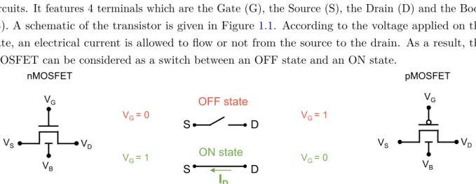
The Metal Oxide Semiconductor Field Effect Transistor (MOSFET) is the key element of integrated circuits. It features 4 terminals which are the Gate (G), the Source (S), the Drain (D) and the Body (B). A schematic of the transistor is given in Figure 1.1. According to the voltage applied on the gate, an electrical current is allowed to flow or not from the source to the drain. As a result, the MOSFET can be considered as a switch between an OFF state and an ON state.
Figure 1.1: Schematic of the MOSFET, made of 4 terminals: Gate, Source, Drain and Body. The
MOSFET is considered of a switch whose state ON or OFF is controlled by the gate voltage VG. An
nMOSFET (pMOSFET) is OFF if VG="0" (VG="1") and turned ON if VG="1" (VG="0"), respectively.
The n- and p-MOSFETs behave complementary, hence the name CMOS technology.
The MOSFET can either be of n- of p-type depending on the carrier type in the source/drain and body. An nMOSFET (also called nMOS or nFET) consists in n-type source and drain, and a p-type body. The major carrier in the source and drain reservoirs are thus electron. It is the opposite for a pMOSFET, featuring p-type source and drain (hole reservoirs) and n-type body.
The nMOSFET is in OFF state if a "0" is applied on its gate. In this case, it acts as an open switch, i.e. no current flows. On the other hand, if a "1" is applied on the gate, the switch is closed, allowing a current to flow between the source and the drain. It is the exact opposite for the pMOSFET, which is in OFF (ON) state if a "1" ("0") is applied on the gate, respectively. As a consequence, the
nMOSFET and pMOSFET are complementary (hence the CMOS technology). This is summarized in Figure1.1.
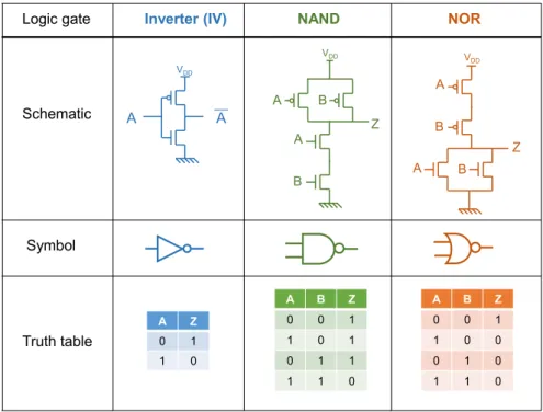
1.1.1.b Boolean functions using logic combinatory gates
In the CMOS technology, the two types of MOSFET are enjoyed to achieve Boolean functions using logic gates. The most simple logic gate is the inverter. As its name indicates, the inverter output is the inverse of its input. The inverter is made with one nMOS transistor and one pMOS transistor, as shown in Figure1.2. The nMOS source is connected to the ground (GND) while the pMOS one is connected to the supply voltage VDD. Both nMOS and pMOS gates are connected to the input (A) and both drains to the output (Z). This way, if the input is "0", the nMOS is OFF and the pMOS ON. The output is thus pulled up to VDD, i.e. "1". If the input is "1", the pMOS is open (i.e. OFF) and the nMOS is closed (i.e. ON), pulling down the output to "0", since it is connected to the ground. The inverter output is thus well given by Z=A.
Figure 1.2: Schematic, symbol and truth table of inverter, NAND and NOR logic gates. The nMOSFET
network is called pull-down because it connects the output to the ground and the pMOSFET network is called pull-up because it connects the output to the supply voltage VDD. The transistors inside networks
are connected in series or in parallel according to the logic function.
Figure1.2 algo gives the schematic, symbol and truth table of the NAND and NOR 2-input logic gates. The NAND logic gate consists in two pMOSFETs in parallel and two nMOSFETs in series. It is the opposite for the NOR gate. The input A is connected to the gate of one pFET and one nFET and the remaining two gates are connected to the second input B. Let us consider a NOR gate. If either A or B is "1", at least one nFET is ON, creating a path from the ground to the output (i.e. Z="0"). The output is pulled-up to VDD if and only if both inputs A and B are "0" since the two pMOS transistors are in series.
Figure 1.3: Schematic of the
OR-AND-INVERT-31 (OAI-OR-AND-INVERT-31) compound gate. The logic function is achieved by relevantly building the pull-down and pull-up networks. Transistors in series in the pull-up network are in parallel in the pull-down network and vice versa.
voltage VDDand the nMOSFET network is called the pull-down because it connects the output to the ground GND. More complex logic functions can be achieved by using pull-up and pull-down networks made of transistors in series or in parallel. Figure 1.3 shows the example of the compound gate achieving the function Z=(A + B + C) · D. This logic compound gate is called OR-AND-INVERT-31 or OAI-31. In the pull-down network, the 3 inputs A, B and C built in parallel are connected in series with the fourth input D. It is the opposite for the pull-up network. The logic function of OAI-31 could have been achieved with several logic gates such as inverter or NOR. However, it would have required to use more transistors. Hence the interest of relevantly using pull-up and pull-down networks.
1.1.2 The Power/Performance/Area metrics
In this section, a focus is made on the Power/Performance/Area (PPA) metrics. These metrics are of great interest to characterize a CMOS technology 1.
1.1.2.a Power/Performance: the ring-oscillator metrics
In a digital integrated circuit, the logic gates are used for operating boolean functions. The circuit speed is directly linked to the ability of the logic gates to perform their operation. The ring-oscillator is a device enabling a dynamic characterization [Sai15]. It consists in a circular chain made of an odd number of inverters. Figure 1.4 shows an example with three inverters. The output of the last inverter is connected to the input of the first inverter. This way, the output is not stable as it will oscillate between the "1" and "0" states (i.e. VDD and GND). The oscillation frequency 𝐹 𝑟𝑒𝑞 (or 𝑓 ) depends on the number of inverters 𝑁 and the propagation delay of each inverter 𝜏𝑃:
𝐹 𝑟𝑒𝑞 = 1
2.𝑁.𝜏𝑃 (1.1)
When the inverter is not switching (i.e. input and output are at a fixed value), the current flowing through the inverter is the leakage current 𝐼𝐷𝐷𝑄. This current is also referred as the stand-by or
static current. It is measured through the supply voltage in the quiescent state (hence the name
1 In addition to the Power/Performance/Area metrics, the Cost, Yield and also Reliability are sometimes also mentioned.
Figure 1.4: (left) symbolic and schematic views of a ring-oscillator made of three inverters. (right)
Voltage at the output of the third inverter as a function of time, oscillating between "1" (VDD) and "0"
(GND) at a frequency 𝑓 . The current flowing through an inverter is composed of the dynamic current
𝐼𝐷𝑌 𝑁 and the static current 𝐼𝐷𝐷𝑄. The dynamic current is the drive current of either the pMOS or the
nMOS to load the output capacitance (i.e. the gates from the next level inverter) during a switching and the static current is the leakage when the inverter is not active.
𝐼𝐷𝐷𝑄). This leakage current is directly linked to the nMOS and pMOS leakage currents 𝐼𝑂𝐹 𝐹,
defined in section1.1.3.
When a stage of inverter is switching because of a change of input, a dynamic current loads the output capacitance. In a ring-oscillator, this dynamic current 𝐼𝐷𝑌 𝑁 is successively generated by
each inverter stage. It flows alternatively through the nMOS (pull-down) and the pMOS (pull-up) according to the switching operation ("0" to "1" or "1" to "0"). 𝐼𝐷𝑌 𝑁 is measured through VDD 1. The delay can be expressed as a function of the dynamic current 2:
𝜏𝑃 =
𝑉𝐷𝐷𝐶𝐸𝐹 𝐹
2 𝐼𝐷𝑌 𝑁 (1.5)
where 𝐶𝐸𝐹 𝐹 is the effective capacitance to be loaded. This capacitance includes the gate capacitance
of the next level inverter (the active part) and all parasitic capacitances (discussed later on in section
1.2.4).
1 Even though no current flows through VDD when the output capacitance is discharged by the nMOS (the current
flows through the output to the ground), it is the exact same current that is injected from the supply voltage to load the capacitance. That is why 𝐼𝐷𝑌 𝑁 can be measured through VDD.
2 Starting from: −𝐼= 𝐶𝐸𝐹 𝐹d𝑉
d𝑡 (1.2)
and by defining 𝐼𝐷𝑌 𝑁 as the average current during the switching and integrating: −𝐼𝐷𝑌 𝑁𝜏𝑃 = 𝐶𝐸𝐹 𝐹
ˆ 𝜏𝑃 0
d𝑉
One can also write:
𝜏𝑃 = 𝑅𝐸𝐹 𝐹𝐶𝐸𝐹 𝐹 (1.6)
with 𝑅𝐸𝐹 𝐹 = 2 𝐼𝑉𝐷𝐷
𝐷𝑌 𝑁.
In terms of power, the dynamic and static powers are deduced from the currents. The dynamic power is given by:
𝑃𝐷𝑌 𝑁 = 𝐼𝐷𝑌 𝑁𝑉𝐷𝐷 =
𝑉𝐷𝐷2· 𝐶𝐸𝐹 𝐹
2 𝜏𝑃 (1.7)
and the static power by:
𝑃𝑆𝑇 𝐴𝑇 = 𝐼𝐷𝐷𝑄𝑉𝐷𝐷 (1.8)
The total power of a circuit depends on the activity factor 𝛼:
𝑃𝑇 𝑂𝑇 = 𝛼𝑃𝐷𝑌 𝑁 + 𝑃𝑆𝑇 𝐴𝑇 (1.9)
This activity factor depends on the application. Finally, the Energy-Delay-Product 𝐸𝐷𝑃 , defined as
𝐸𝐷𝑃 = 𝐸 · 𝜏𝑃 = 𝑃𝑇 𝑂𝑇 · 𝜏𝑃 · 𝜏𝑃 (1.10)
is a good figure of merit for energy efficient circuits. Its minimum translates the sweet point between consumption and performance.
1.1.2.b Area: standard cell design
In the previous paragraph, the dynamic power/performance metrics have been presented. In this paragraph, the last term of PPA, i.e. the Area, is discussed by the means of a typical layout of a standard cell. A standard cell consists in a physical implementation of a function operated by transistors. Standard cells include combinatory logic (e.g. inverter, NAND, NOR) and sequential logice or storage (e.g. flipflops) functions. Figure 1.5 shows the layout of the 1-finger inverter standard cell (also called IV-SX1).
The main layers are represented on the layout: active area (RX), gate (or poly, PC), active contact (CA), gate contact (CB), first level of metal (M1). The active areas are isolated from each other by the means of Shallow Trench Isolation (STI). The pMOS and nMOS sources are connected to the power rails (power supply VDD for pMOS and ground GND for nMOS). The function of a standard cell is determined by the way the transistors are connected to each other with the metal lines. In
which leads to:
−𝐼𝐷𝑌 𝑁𝜏𝑃 = 𝐶𝐸𝐹 𝐹[𝑉 (𝜏𝑃) − 𝑉 (0)] = 𝐶𝐸𝐹 𝐹 [︂ 𝑉𝐷𝐷 2 − 𝑉𝐷𝐷 ]︂ ⇔ 𝜏𝑃 = 𝑉𝐷𝐷𝐶𝐸𝐹 𝐹 2 𝐼𝐷𝑌 𝑁 (1.4)
Figure 1.5: Layout of the 1-finger
in-verter standard cell. The pMOS and nMOS are designed between the two power rails. The standard cell height is expressed as a function of the number of Metal-1 pitches and its width is expressed as a function of the number of poly pitches (CPPs).
the case of the inverter, the pMOS and nMOS drains are connected to the output. In an integrated circuit, the standard cells are abutted to each other and can be flipped in order to share the power rails.
The area of a standard cell is defined by its height and width. The height is expressed as a function of the number of M1 pitches (M1P), also called tracks1, and the width as a function of the number of Contacted Poly Pitches (CPPs). The product M1P×CPP is therefore a good figure of merit of a technology density, i.e. node. The area of the Static Random Access Memory (SRAM) cell (see appendix B) is also a good indicator of a technology density.
In advanced technologies, efforts have been made on the optimization of the standard cell rather than only focusing on the transistor. This is referred as the Design/Technology Co-Optimization (DTCO).
1.1.3 The MOSFET operation and metrics
In the previous section, the MOSFET has been presented as an ideal switch that is used in the CMOS technology to perform logic operations. The aim of this section is to provide some insights about the MOSFET operation and the main metrics used in this work. A more detailed theory and modeling of the MOSFET transistor can be found in [Sko00] and [Hu10].
1.1.3.a The MOSFET structure
An illustration of a MOSFET device is shown in Figure 1.6. The control electrode, i.e. the gate, consists in a Metal Oxide Semiconductor (MOS) capacitance, whose geometry is defined according to the gate length L and transistor width W. The gate oxide is characterized by its thickness 𝑡𝑜𝑥,
which is crucial for the device performance. The two reservoirs of carrier, i.e. the source and drain,
are placed at each side of the gate. Figure 1.6also shows a typical layout of a transistor. The active area is represented in green and the gate in red.
Figure 1.6: Illustration of typical MOSFET (left) cross-section and (right) top-view, i.e. layout.
1.1.3.b The MOSFET operation
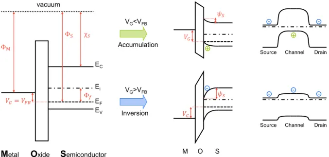
The MOS capacitance can operate in different regimes, according to the potential at the semiconduc-tor/oxide interface 𝜓𝑠, dependent on the gate voltage VG. Let us consider a MOS with a p-type semiconductor, which is the case of the nMOSFET. The three regimes are:
• The accumulation (𝜓𝑠< 0 ; 𝑉𝐺 < 𝑉𝐹 𝐵). The majority carrier (holes in a p-type substrate) are
attracted by the electric field towards the gate. The flat-band voltage 𝑉𝐹 𝐵 is defined as the gate voltage that must be applied in order to have a flat energy band in the semiconductor, (i.e. no charge in the capacitor). Figure 1.7 shows the band diagram of the MOS structure under flat-band condition and accumulation. The band diagram from the source to the drain is also represented. A barrier of potential prevents the electron to flow from source to drain. The MOSFET is in OFF state.
• The depletion (0 < 𝜓𝑠 < 𝜑𝑓 ; 𝑉𝐺 > 𝑉𝐹 𝐵). 𝜑𝑓 is the Fermi potential, given by 𝜑𝑓 = 𝑘𝑇 𝑞 ln (︁ 𝑁𝐴 𝑛𝑖 )︁
where 𝑁𝐴 is the dopant concentration is the substrate. Under the depletion regime,
majority carriers are pushed away from the oxide/semiconductor interface. The charge in the semiconductor is due to the ionized dopants (negative charge in the case of an nMOSFET). • The inversion (𝜓𝑠 > 𝜑𝑓 ; 𝑉𝐺 >> 𝑉𝐹 𝐵) or strong inversion (𝜓𝑠 > 2 · 𝜑𝑓). In inversion, the
previously minority carriers become more numerous. In strong inversion, there are more minority carriers (electrons) than majority carriers (holes) in the bulk. A conduction path, called the channel, appears. The electrons are allowed to flow between the source and drain as illustrated in Figure1.7. The MOSFET is in ON state.
The threshold voltage is defined as the criterion of strong inversion. In the case of the historical planar bulk1 technology, the threshold voltage is defined by :
𝑉𝑇 = 𝑉𝐹 𝐵 + 2𝜑𝑓 +
𝑄𝑑𝑒𝑝
𝐶𝑜𝑥
(1.11)
Figure 1.7: (left) Band diagram of the MOS structure under flat band condition. 𝜑𝑀 and 𝜑𝑆 are the
metal and semiconductor work functions, respectively. 𝜒𝑆 is the electron affinity. 𝜑𝑓 is the Fermi potential. 𝐸𝐹 is the Fermi level. 𝐸𝑖 is the intrinsic Fermi level. 𝐸𝐶 is the bottom of the conduction band and 𝐸𝑉
the top of the valence band. (right) Band diagrams of a MOSFET in (top) accumulation or OFF state, i.e. no current from source to drain, and (bottom) inversion or ON state, i.e. carriers are free to flow from source to drain because of the reduced potential barrier.
where 𝑉𝐹 𝐵 = 𝜑𝑀 −
(︁
𝜒𝑆+𝐸2𝑔 + 𝜑𝑓
)︁
, 𝑄𝑑𝑒𝑝 is the charge of depletion and 𝐶𝑜𝑥 the gate oxide
capacitance.
1.1.3.c The MOSFET principal metrics
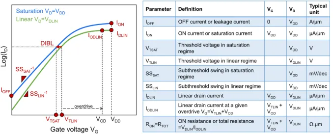
The ideal MOSFET switch is closed (i.e. ON) if the gate voltage is above 𝑉𝑇 and open (i.e. OFF) otherwise. Actually, a real MOSFET is not an ideal switch. It exhibits a leakage current in OFF state, a relatively smooth transition from OFF to ON states, and can provide a limited current in ON state. This is illustrated on the 𝐼𝐷(𝑉𝐺) curve in log scale, also called transfer characteristic, of Figure1.8. Two regimes are distinguished:
• The linear regime, where the voltage applied on the drain is small (typically less than 50mV) • The saturation regime, where the voltage applied on the drain is VDD.
A MOSFET is characterized by different parameters that allow its performance to be evaluated. Most of these parameters can be directly extracted from electrical measurements. The table of Figure
1.8defines the main electrical characteristics of a transistor.
As far as the threshold voltage is concerned, it is usually extracted at a given current of value 𝐼𝑡ℎ, whose value is typically 100nA·𝑊𝐿. In the subthreshold regime, the drain current increases
exponentially with the gate voltage. We can express the drain current as:
𝐼𝐷 = 𝑊 𝐿 𝜇0𝐶𝑑𝑒𝑝 (︂ 𝑘𝑇 𝑞 )︂2(︂ 1 − exp(︂ −𝑞𝑉𝐷 𝑘𝑇 )︂)︂ · (︃ exp (︃ 𝑞 𝑉𝐺− 𝑉𝑇 (1 +𝐶𝑑𝑒𝑝 𝐶𝑜𝑥)𝑘𝑇 )︃)︃ (1.12)
Figure 1.8: (left) MOSFET 𝐼𝐷(𝑉𝐺) curves in linear and saturation regimes, also called transfer
characteristics. (right) Table of the main electrical metrics of the MOSFET, also shown on the 𝐼𝐷(𝑉𝐺)
curve.
where 𝜇0 is the low-field mobility and 𝐶𝑑𝑒𝑝 the capacitance of depletion.
The subthreshold swing 𝑆𝑆, translating the exponential increase of the drain current with respect to the gate voltage, is defined as:
𝑆𝑆 = d𝑉𝐺
d log(𝐼𝐷) (1.13)
and can be expressed according to 1.12as:
𝑆𝑆 = 𝑘𝑇 𝑞 ln(10) d𝑉𝐺 d𝜓𝑆 = 𝑘𝑇 𝑞 ln(10) (︂ 1 +𝐶𝑑𝑒𝑝+ 𝐶𝑠𝑠 𝐶𝑜𝑥 )︂ (1.14)
where 𝐶𝑠𝑠is the capacitance related to the surface states. By neglecting 𝐶𝑠𝑠and 𝐶𝑑𝑒𝑝 the theoretical
subthreshold swing is 𝑆𝑆=60mV/dec. The subthreshold swing is a good indicator of the electrostatic control. The current in the subthreshold regime can be expressed according to the subthreshold swing by: 𝐼𝐷 = 𝐼𝑡ℎexp (︂ 𝑉𝐺− 𝑉𝑇 𝑆𝑆/ ln(10) )︂ (1.15)
which leads to the expression of the leakage current (assuming an OFF state in the subthreshold regime): 𝐼𝑂𝐹 𝐹 = 𝐼𝑡ℎexp (︂ −𝑉 𝑇 𝑆𝑆/ ln(10) )︂ (1.16)
In the strong inversion, the linear drain current can be written as:
𝐼𝐷 = 𝑊 𝐿𝜇𝑒𝑓 𝑓𝐶𝑜𝑥 (︂ 𝑉𝐺− 𝑉𝑇 − 𝑉𝐷 2 )︂ 𝑉𝐷 (1.17)
with 𝜇𝑒𝑓 𝑓 the effective mobility of the carriers in the channel. More details about the physics of carrier mobility is given in section1.1.3.g.
Rather than the linear drain current, the 𝐼𝑂𝐷𝐿𝐼𝑁 current is preferred in order to have an image of
the mobility in a MOSFET device. The 𝐼𝑂𝐷𝐿𝐼𝑁 current is measured at a given overdrive (𝑉𝐺− 𝑉𝑇). This way, the current value is free from threshold voltage variation.
The historical metric of performance is the ON current 𝐼𝑂𝑁, also called the saturation current. It is
the drain current at 𝑉𝐺= 𝑉𝐷 = 𝑉𝐷𝐷.
1.1.3.d The effective drive current in an inverter
Actually, in an inverter, the input and output voltages vary as the MOSFET current is loading the output capacitance. In other words, the MOSFET does not operate at a given bias configuration in dynamic. The parameters presented in Figure1.8are all DC parameters, i.e. obtained from static measurements. Na et al. [Na02] proposed a DC approximation of the drive current in an inverter. The inverter switching delay 𝜏𝑃 is defined as the delay between the point where the input voltage
𝑉𝐼𝑁 = 𝑉𝐷𝐷2 and the point where the output voltage 𝑉𝑂𝑈 𝑇 = 𝑉𝐷𝐷2 . This is represented in Figure1.9.
Figure 1.9: Illustration of the effective drive current in an inverter [Na02]. 𝐼𝐸𝐹 𝐹 is a DC approximation
of the average drain current during the switching delay 𝜏𝑃 (also called propagation delay).
The effective drive current 𝐼𝐸𝐹 𝐹 is the average of the drain current during the switching. It is approximated by: 𝐼𝐸𝐹 𝐹 = 𝐼𝐻 + 𝐼𝐿 2 (1.18) where ⎧ ⎪ ⎪ ⎨ ⎪ ⎪ ⎩ 𝐼𝐻 = 𝐼𝐷 [︁ 𝑉𝐺= 𝑉𝐷𝐷 ; 𝑉𝐷 = 𝑉𝐷𝐷2 ]︁ 𝐼𝐿= 𝐼𝐷 [︁ 𝑉𝐺 = 𝑉𝐷𝐷2 ; 𝑉𝐷 = 𝑉𝐷𝐷 ]︁ (1.19)
Although the 𝐼𝐸𝐹 𝐹 current is a relevant approach, it has been shown that it can deviate from the
1.9is impacted by the capacitance to load.
1.1.3.e The importance of the electrostatic control
In a short channel MOSFET, the control of the channel potential by the gate is not as efficient as for long channel devices. This is illustrated in Figure 1.10. The Short Channel Effect (SCE) translates the fact that the shorter the gate length, the lower the barrier from the source to the channel. This is due to the band curvature induced by the source-channel and drain-channel PN junctions and results in a lower threshold voltage for short channel devices.
Figure 1.10: Top of the band schematic. The potential barrier is lowered for short channel (Short
Channel Effect, SCE) and under a drain bias (Drain-Induced Barrier Lowering, DIBL).
In addition, the barrier further reduces when a high voltage is applied on the drain. This effect is called the Drain-Induced Barrier Lowering (DIBL). The DIBL is thus defined as the difference between the threshold voltage extracted in linear regime 𝑉𝑇 𝐿𝐼𝑁 and the one extracted in saturation
regime 𝑉𝑇 𝑆𝐴𝑇: DIBL = ⃒ ⃒ ⃒ 𝑉𝑇 𝑆𝐴𝑇 − 𝑉𝑇 𝐿𝐼𝑁 𝑉𝐷𝑆𝐴𝑇 − 𝑉𝐷𝐿𝐼𝑁 ⃒ ⃒ ⃒ (1.20)
The DIBL is also sometimes expressed in mV according to 𝐷𝐼𝐵𝐿 = |𝑉𝑇 𝑆𝐴𝑇 − 𝑉𝑇 𝐿𝐼𝑁|. A low DIBL
value is an evidence of a good electrostatic control. It is crucial for the performance of the MOSFET since it impacts its effective drive current. At a given leakage 𝐼𝑂𝐹 𝐹 and ON current 𝐼𝑂𝑁, the 𝐼𝐻
current is strongly impacted by the DIBL, as illustrated in Figure 1.11(because of higher 𝑉𝑇 for 𝑉𝐷=𝑉𝐷𝐷/2 than for 𝑉𝐷=𝑉𝐷𝐷).
1.1.3.f The performance/leakage trade-off
Finally, the main figure of merit of the MOSFET is the trade-off between performance and leakage (Figure 1.12). The best performance, i.e. the highest effective drive current, is wanted at the lowest leakage. A CMOS technology offers different VT flavors in order to cover a large range of performance/leakage. This is interesting for designing efficient circuits, depending on the application 1. High-V
T (HVT) are suitable for low power and Low-VT (LVT) for high performance.
1 Mixing different VTflavors is also efficient for enhancing the circuit performance thourgh critical path optimization
Figure 1.11: Illustration of the impact of the
DIBL on the effective current 𝐼𝐸𝐹 𝐹. A weak
elec-trostatic control, i.e. high DIBL, is translated into
𝐼𝐸𝐹 𝐹 degradation (same leakage is considered).
Figure 1.12: Performance/Leakage trade-off. A large range is covered thanks to multi VT
flavors (HVT=High-VT, RVT=Regular-VT and
LVT=Low-VT).
1.1.3.g The crucial role of carrier mobility
The mobility 𝜇 characterizes the ability of a carrier (electron or hole) to move under an electric field 𝐸. The drift velocity is therefore given by:
𝑣𝑑= 𝜇𝐸 (1.21)
In a semiconductor, the carriers experience several scattering mechanisms. Among them, the main scattering mechanisms present in a MOSFET channel are:
• Remote Coulomb scattering or interactions with ionized impurities (or any charged element like traps for instance). The ionized impurities in a MOSFET are typically the dopants. As a carrier is flowing, it can be deflected by the Coulomb forces induced by a ionized dopant. • Phonon scattering. Phonons are acoustic waves created by the vibrating atoms of the crystal
lattice. The more the carriers are interacting with phonons, the lower the mobility. At low temperature, the crystal vibration is decreased, which results in less phonons and thus in higher mobility.
• Surface Roughness scattering. The roughness of the oxide/semiconductor interface causes fluctuations of the energy levels. The more the carrier are located close to the interface, the more they are subjected to surface roughness scattering. Such a scattering mechanism thus limits the carrier mobility especially under high transverse electric field (i.e. in strong inversion). These scattering mechanism dependence with the transverse field and the temperature are different [Che96;Tak94b].
The carrier mobility can be given by:
𝜇 = 𝑞 · 𝜏
𝑚* (1.22)
scattering time or average free time of flight) and 𝑚* the effective mass. The carriers in the crystal are not free since they interact with the lattice. The effective mass is the mass of the carrier assumed to be free and accounting for the aforementioned interactions with the crystal. It can be derived from the curvature of the band structure E(k):
E(k) = E0+~ 2k2
2𝑚* (1.23)
In an operating MOSFET, the carriers can be subjected to several sources of scattering at the same time. The Matthiessen’s rule allows to combine their effects according to:
1 𝜇 = ∑︁ 𝑖 1 𝜇𝑖 (1.24)
with 𝜇𝑖 the mobility associated to the 𝑖 scattering mechanism. The Matthiessen’s rule is an approximation since it assumes no interaction between the different scattering mechanisms.
Figure 1.13 illustrates the electron effective mobility in a MOSFET according to the effective transverse field. The transverse field 𝐸𝑒𝑓 𝑓 is given by:
𝐸𝑒𝑓 𝑓 =
𝜂𝑄𝐷𝐸𝑃 + 𝑄𝐼𝑁 𝑉
𝜀𝑆𝑖
(1.25)
where 𝜂 is an empirical parameter relating the average field in the inversion layer and whose value is 1/2 for electrons and 1/3 for holes. Under high transverse field, the mobility is not impacted by the remote Coulomb scattering. It is thus independent of the doping level. The mobility of Si/SiO2 MOSFETs follows an universal mobility trend with respect to the effective field [Tak94a;Tak94b]. In a CMOS technology, there are numerous elements that can affect the scattering mechanisms such as the level of doping in the substrate, the metal used in the gate stack or the level of strain in the device. The latter will be discussed in section 1.3.2.
Actually, the equation 1.21 is no longer valid under a high longitudinal electric field. When the carrier exhibits a high kinetic energy, the interaction with phonons is predominant and the carrier velocity saturates. The saturation velocity 𝑣𝑠𝑎𝑡 is typically ≈107cm/s for electrons in Silicon and the
critical electric field is approximately ≈104V/cm. If the carrier velocity is limited by 𝑣𝑠𝑎𝑡, the drain current is expressed as:
𝐼𝐷 = 𝑊 𝑄𝐼𝑁 𝑉 𝑣𝑠𝑎𝑡 (1.26)
In the current CMOS technologies, short channel devices are operating close to the saturation regime. The carrier mobility may not be the most relevant indicator of performance. Nevertheless, it has been showed that the saturation current is still highly correlated to the mobility in short channel devices [And05;Loc02].
The transport can also be discussed under ballistic considerations. If the channel length is shorter than the mean free path between two scattering events, the carriers can move from the source to
Figure 1.13: Illustration of the electron effective
mobility dependence with the transverse electric field. The total mobility is derived from the three components (remote Coulomb, phonons, surface roughness) according to Matthiessen’s law. The dependence with temperature and field is specific to each scattering mechanism [Che96;Tak94b].
Figure 1.14: Carrier velocity as a function of the
longitudinal electric field. Below the critical field, the velocity is directly proportional to the field through mobility. The velocity saturates under high field.
the drain without experiencing any interaction. In that case, the current is limited by the injection velocity 𝑣𝑖𝑛𝑗:
𝐼𝐷 = 𝑊 𝑄𝐼𝑁 𝑉 𝑣𝑖𝑛𝑗 (1.27)
This expression can been used to reproduce the transistor characteristics with the help of a simple compact model [Kha09]1.
If only a part of the carriers experiences ballistic transport, it can be relevant to introduce the channel back-scattering coefficient 𝑟 (which depends on the mobility) and write the expression of the current as [Lun01]: ⎧ ⎪ ⎪ ⎨ ⎪ ⎪ ⎩ 𝐼𝐷 = 𝑊 𝑄𝐼𝑁 𝑉 𝑣𝑇 2𝑘𝑇 /𝑞(1 − 𝑟) 𝑉𝐷 ; 𝑟 = 𝐿 𝐿 + 𝜆0 in linear regime 𝐼𝐷 = 𝑊 𝑄𝐼𝑁 𝑉 𝑣𝑇 (︂ 1 − 𝑟 1 + 𝑟 )︂ ; 𝑟 = ℓ ℓ + 𝜆0 in saturation regime (1.28)
where 𝑣𝑇 is the thermal velocity, 𝜆0 is the mean free path and ℓ the distance for the potential to drop by 𝑘𝑇 /𝑞.
Despite the different approaches for dealing with the transport under a high longitudinal field, it is commonly accepted that mobility still plays a significant role on the transport [Ant06; Kha13;
Sai09]. Especially, the velocity is correlated to the effective mass and so is the mobility. The mobility remains a good indicator of the intrinsic performance of the MOSFET.
1 The model of Khakifirooz et al. [Kha09] has been used in section4.3.2to compare MOSFETs of two different integration schemes.
1.2 CMOS technology scaling: the king is dead, long live the king !
The well-known "scaling" has been the driving force for improving the Power/Performance/Area and most of all Cost metrics discussed in the previous section. Nevertheless, the task has become more and more challenging over the years. This section gives a brief historic review of the CMOS technology scaling and presents the main limitations.1.2.1 The happy scaling, the good old days
When discussing about CMOS scaling, Moore’s law is inevitable [Moo65]. Moore observed that there is an optimum number of components for achieving the lowest cost per component (Figure 1.15). This optimum results from the positive impact of miniaturization and the negative impact of yield degradation when the circuit becomes too complex. From this observation, Moore predicted that
the number of transistors on a chip would double every two years. At the time, Moore’s
projection was based on the data from 1959 to 1965 and was projected until 1975 (Figure 1.15). It has been proven accurate for several decades. Reducing the size of transistors and therefore the size of a chip for a given functionality results in a cost reduction. This has been the driving force of the CMOS technology scaling. Manufacturers adopted Moore’s law as a roadmap for setting the next generation targets.
Figure 1.15: (left) Optimum number of components for achieving the lowest cost per component. (right)
Moore’s projection about the exponential growth of the number of transistors per integrated circuit over the years [Moo65]. Figures from [Moo06].
By cramming more components on a die, the functionality of the circuit is increased. The improvement in terms of performance was later discussed by Dennard et al. [Den74]. Scaling the transistor
dimensions (gate length, width and oxide thickness) by a constant factor 𝜅 provides a delay improvement at a constant power density (Figure1.16). Transistors enjoyed Dennard’s scaling until the 130nm node. This period is today referred as the "happy scaling" since cost, functionality and performance benefit from dimension reduction without any trade-off.
Figure 1.16: Dennard’s scaling: Reducing the transistor dimensions (gate length, width and oxide thick-ness) by a constant factor 𝜅 provides a delay improvement at a constant power density. Scaling according to Moore’s and Dennard’s laws is ref-ered as the "happy scaling" since cost, functionality and performance bene-fit from dimension reduction. Figure from [Den74].
1.2.2 The introduction of goodies
For sub-100nm nodes, the performance gain from Dennard’s happy scaling reached a limit. Dennard’s assumptions were no longer valid and parasitic effects from dimension reduction appeared.
Especially, the threshold voltage must be reduced by a factor 𝜅 without degrading the leakage. This imposes an improvement on the subthreshold swing, yet limited to 60mV/decade. Since the threshold voltage can not follow the supply voltage scaling, the gate overdrive (VDD-VT) decreases for a constant static consumption. In order to compensate for the drive loss while supply voltage is scaled, additional knobs to boost the performance are used. Intel introduced mechanical stress in their 90nm technology [Gha03;Tho04] (Figure1.17). Stress is an efficient way to boost the carrier mobility, as discussed in section1.3.2. This enables a performance improvement without degrading the leakage.
Figure 1.17: First stress
in-troduction in Intel’s 90nm tech-nology [Gha03][Tho04]. Both pMOS and nMOS benefit from local stress introduction. Compressive stress from SiGe source/drain is used for the pMOS and tensile stress from a stressed SiN film is used for nMOS. Figure from [Tho04].
Then, the reduction of the gate oxide thickness needed for current improvement (and short channel effect control) comes along with increased gate leakage from tunneling currents. The introduction of a "high-𝜅" (or high-k) dielectric allowed to increase to gate oxide capacitance 𝐶𝑜𝑥 without reducing the oxide physical thickness 𝑡𝑜𝑥 by taking advantage of a higher dielectric constant 𝜅 than conventional
SiO2 (𝜅𝑆𝑖𝑂2 = 3.9). The Equivalent Oxide Thickness (EOT) is defined as the thickness of SiO2 giving the same capacitance as the one of a "high-𝜅" dielectric of thickness 𝑡high−𝜅:
𝐸𝑂𝑇 = 𝑡high−𝜅 𝜅𝑆𝑖𝑂2 𝜅high−𝜅
(1.29)
in Figure 1.18 [Mis07].
Figure 1.18: High-𝜅 introduction at the 45nm node, from [Mis07]. (left) Gate stack with high-𝜅 dielectric and metal gate. (right) Gate leakage reduction with high-𝜅 introduction because of a thicker oxide at a constant capacitance.
1.2.3 The rise of new architectures
As discussed in section 1.1.3.e, the electrostatic control of the channel by the gate is degraded for short channels. This is due to a parasitic coupling from drain to source. As previously discussed, the DIBL impacts the performance. It is therefore mandatory to maintain a good electrostatic control in order to achieve high performance at a given leakage. New architectures have been developed, relying on multi-gate transistors [Fer11]. These architectures have replaced the historical bulk planar transistors for sub-30nm technologies.
1.2.3.a The FinFET
The FinFET consists in a 3D transistor where the gate wraps a channel fin, as illustrated in Figure
1.19. The first report of a FinFET device was made by Hisamoto et al. [His98] (called "folded-channel" transistor). It was first manufactured by Intel at the 22nm node [Aut12;Jan12] and became mainstream for the next nodes (TSMC’s 16nm [Wu13], Intel’s 14nm [Jan15; Nat14], GlobalFoundries’ 14nm, Samsung’s 14nm [Son14] and 10nm [Cho16;Seo14]).
Figure 1.19: FinFET schematic. The FinFET is a
3D transistor where the gate is wrapped around the fin-shaped channel. A FinFET is also referred as a tri-gate transistor. Figure from Intel.
The FinFET features a thin channel, which is fully depleted. It can be seen as a double-gate device or tri-gate if the top width is taken into account. The FinFET architecture provides a good electrostatic control and therefore makes it more immune to short channel effects.
Figure 1.20: (a) FinFET SEM tilted top view, emphasizing the 3D architecture, from [Aut12]. (b) Cross-section in the gate of FinFET from 14nm node [Nat14], showing the FinFET height, top width and footprint. (c) Cross-section along the source/drain direction, from [Aut12].
In addition, an other strength of the FinFET relies on the effective width of the transistor, defined by:
𝑊𝐸𝐹 𝐹 = 𝑊𝑇 𝑂𝑃 + 2 · 𝐻 (1.30)
where 𝑊𝑇 𝑂𝑃 is the top width and 𝐻 the height of the fin (see Figure 1.20). The 3D channel yields increased transistor width at a given footprint, especially for aggressive fin pitches. This results in high drive current, which is required for high performance, and also a reduced variability. Nevertheless, achieving high density is challenging and costly since it requires multiple patterning. The fins are indeed fabricated by Sidewall Image Transfer (SIT), also called spacer patterning or Self Aligned Double Patterning (SADP).
FinFET is today still seen as a viable option for sub-10nm nodes (TSMC’s 7nm [Wu16], IBM’s 7nm technology [Xie16]).
1.2.3.b The FDSOI technology
The Fully Depleted Silicon On Insulator (FDSOI) technology refers to the use of a SOI substrate instead of a bulk Silicon substrate. The SOI substrate is fabricated by the Smart Cut technique which relies on direct bonding [Bru95]. If the Silicon film is thin enough, it is fully depleted1. In this case, the depletion thickness and the junction depth are equivalent to the film thickness. This results in an enhanced electrostatic control with respect to planar bulk technologies.
Nevertheless, a coupling between the drain and the channel occurs through the buried oxide (BOX) [Ern07]. The thinnest the BOX thickness and the highest the Ground Plane (GP) doping, the more this effect is mitigated [Gal06]. The electrostatic control is maximized for thin Silicon film and BOX, hence the Ultra-Thin Body and Buried oxide Fully-Depleted Silicon On Insulator technology (UTBB-FDSOI).
Figure 1.21: FDSOI transistor schematic, from
STMicro-electronics. The transistor is built on a Silicon On Insulator (SOI) substrate. The thin Silicon film and buried oxide (BOX) allow a good electrostatic control. The channel-body coupling due the BOX enables a high back-bias efficiency.
Figure 1.22: Cross-section of a FDSOI
transistor from 28nm technology. The film thickness 𝑡𝑆𝑖 is 7nm. Figure from
[Pla12].
Figures 1.21 and 1.22 present a transistor from UTBB-FDSOI technology. The UTBB-FDSOI technology has been developed at the 28nm node [Pla12] and 14nm node [Web14; Web15] by STMicroelectronics/LETI and at the 22nm node by GlobalFoundries/LETI [Car16]. More details about 28nm and 14nm FDSOI technologies are given in section 3.1, with a specific focus on 14nm, which is at the heart of this thesis work.
For thin film devices as in FDSOI, the threshold voltage criterion 𝜓𝑠 > 2 · 𝜑𝑓 (see section 1.1.3.b) is
not relevant as the depletion charge is limited by the film thickness. This criterion has been changed to 𝐶𝑖𝑛𝑣 = 𝐶𝑜𝑥, i.e. the capacitance of inversion equals the one of the gate oxide [Poi05]. This leads
to the expression of the threshold voltage [Poi05]:
𝑉𝑇 = 𝑉𝐹 𝐵 + 𝑘𝑇 𝑞 ln (︂ 2 · 𝐶𝑜𝑥· 𝑘𝑇 𝑞2· 𝑛 𝑖· 𝑡𝑆𝑖 )︂ + ~ 2· 𝜋2 2 · 𝑞 · 𝑚*· 𝑡𝑆𝑖2 (1.31)
where 𝑡𝑆𝑖 is the SOI thickness and 𝑚* the effective mass of confinement. The last term translates
the effect of the confinement induced by the quantum well formed by the thin silicon layer between the two dielectrics.
In FDSOI, there is a strong coupling between the channel and the body, thanks to the buried oxide. The threshold voltage is therefore highly sensitive to the back-bias and Ground Plane GP doping [And10;Fen09; Web10]. The body factor 𝛾 is defined by the threshold voltage variation with respect to the voltage applied on the body (i.e. the back-bias). Assuming an inversion at the gate oxide/channel interface, neglecting the depletion in the ground plane and considering a capacitance divider, the back-bias efficiency on long channels can be expressed as [Lim83;Noe11]:
𝛾 = 𝛥𝑉𝑇 𝑉𝐵
= 𝐶𝐵𝑂𝑋· 𝐶𝑆𝑖 𝐶𝑂𝑋(𝐶𝐵𝑂𝑋+ 𝐶𝑆𝑖)
(1.32)

![Figure 1.48: Local Layout Effect induced by embedded SiGe source/drain, from [ Son12 ]](https://thumb-eu.123doks.com/thumbv2/123doknet/2114095.8078/60.892.101.430.129.418/figure-local-layout-effect-induced-embedded-sige-source.webp)