HAL Id: hal-00591008
https://hal.archives-ouvertes.fr/hal-00591008
Submitted on 6 May 2011
HAL is a multi-disciplinary open access
archive for the deposit and dissemination of
sci-entific research documents, whether they are
pub-lished or not. The documents may come from
teaching and research institutions in France or
abroad, or from public or private research centers.
L’archive ouverte pluridisciplinaire HAL, est
destinée au dépôt et à la diffusion de documents
scientifiques de niveau recherche, publiés ou non,
émanant des établissements d’enseignement et de
recherche français ou étrangers, des laboratoires
publics ou privés.
An High Performance Integrated Balun for 60 GHz
Application in 65nm CMOS Technology
Mariano Ercoli, Michael Kraemer, Daniela Dragomirescu, Robert Plana
To cite this version:
Mariano Ercoli, Michael Kraemer, Daniela Dragomirescu, Robert Plana. An High Performance
Inte-grated Balun for 60 GHz Application in 65nm CMOS Technology. Asia Pacific Microwave Conference
(APMC 2010), Dec 2010, Yokohama, Japan. p.1845-1848. �hal-00591008�
An High Performance Integrated Balun for 60 GHz Application in
65nm CMOS Technology
Mariano Ercoli
#∗1, Michael Kraemer
#∗2, Daniela Dragomirescu
#∗3, Robert Plana
#∗4#CNRS; LAAS; 7 avenue du colonel Roche F-31077 Toulouse, France
University of Toulouse; UPS, INSA, INP, ISAE, LAAS; F-31077 Toulouse, France
1 mercoli@laas.fr 2 mkraemer@laas.fr 3 daniela@laas.fr 4 plana@laas.fr
Abstract— This paper shows a new design approach that allows
to integrate an efficient balun into mm-wave radio frequency integrated circuits (RFIC). The proposed device is an evolution of the simple transformer. Thanks to the modification on the device’s shape, the performance increases considerably, main-taining limited dimensions. The proposed balun shows a very good power division with only 0.5 dB of maximum amplitude imbalance within the whole band of interest and less than 10°phase imbalance around 60 GHz. The measurement campaign confirms the accuracy of the electromagnetic simulations and the behaviour of the device. The balun is implemented in ST Microelectronic’s 65nm bulk CMOS technology and is employed in a double balanced 60 GHz down-conversion mixer to provide the balanced the LO and RF signal.
Index Terms— Balun, differential balanced transformer, millimetre-wave devices.
I. INTRODUCTION
In mm-wave circuit design, the use of balanced architectures in the transceiver components is strongly beneficial. The ben-efits, like improvement of noise immunity [1], resulting from these architectures, often justify the increase of the number of active components and the higher power consumption. The most common applications of differential architectures are mixers, voltage-controlled oscillators (VCO) and single-stage or multi-stage input and output amplifiers. Often input and output signals are only available in single ended form, so a structure that converts them into differential signal is needed. The behaviour of the single-ended-to-balanced transformation becomes crucial when determining the performance of the en-tire transceiver. There are several examples for the importance of the conversion:
1) In a mixer: an unbalanced power division of the LO sig-nal causes asymmetry of the control sigsig-nal that drives the switching block. The conversion gain of the mixer drops and, increasing non-linearity, degrades the performance. Even a phase imbalance influences the behaviour of the mixer: the phase error leads to degradation of the signal isolation of the structure.
2) In a single or multi stage amplifier: a non-optimal power splitting degrades the performance of a differential am-plifier. An excessive imbalance can generate a saturation of one of the two sides while the other one is still far
from the compression. The phase imbalance decreases the combined signal’s power at the output.
To avoid these issues, different architectural solutions exist when designing a balun. The active balun solution is good, thanks to its very limited occupied area, but in the 60GHz band the problem of common mode rejection is very difficult to solve. A passive structure instead, is not effected from this problem.
In literature tree different classes of passive balun are described: the Marchand Balun, the Rat-race Hybrid and transformers. The size of the classical Marchand Balun and the Rat-race configuration are proportional to the wave length of the signal. In 60 GHz RFIC’s the chip surface dedicated to build these types of device is excessive. Moreover, wide passive circuits in silicon bulk technology show high losses and consequently thermal noise. To reduce the occupied area while maintaining good performance for the balun, the trans-former architecture is often employed [1]. This solution can perform two different actions, imbalanced to balanced signals conversion and impedance matching between different blocks.
II. DESIGN
A. Transformer Features
Dickson et al. show in [1] that it is possible to build trans-former structures in the 60 GHz frequency band that achieve a very high coupling factor for extremely limited dimensions. This is an important property that can be further improved by the use of a stacked coil configuration. The superposition of the primary and secondary coils into different metal layers reduces the covered silicon surface of the transformer and increases the density and the regularity of the magnetic field in the centre of the component. For a planar transformer, with primary and secondary coils in the same layer, [1] shows a coupling factor k of around 0.5. Instead, for stacked transformers, (k) can be close to 0.75 and even higher. In [1] the occupied area for the structure, including the free space around the coils, is a square with a lateral dimension of less than 60µm, while the external coil diameter is only 30 µm.
B. Balun Structure Design
The small size of the component and its high value of k make of the integrated transformer [1] an ideal instrument to
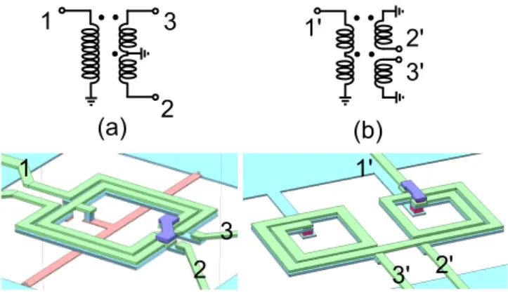
develop a balun with reduced dimensions and high perfor-mance. Transformer showed in Figure 1 (a) has the secondary coil connected directly to a component with differential input (ports 2 and 3). This configuration generates a virtual ground in correspondence of the middle of the output coil (b). The
2
3
1
2
3
1
Virtual Ground (a) (b)Fig. 1. Ideal behaviour for a transformer balun
virtual ground guaranties an equal power splitting and a 180°of phase shift for each output signal. Simulations show that the real behaviour of the transformer balun is very far from the ideal one. This is due to the presence of a parasitic phenomena that modify the ground constraint. The main problem, when using transformer as a balun, is the control of these effects. The amplitude and phase balance depends on the proper behaviour of the ground at the secondary coils. Fig. 2(a) shows a first example of modified transformer employed as a balun: while the single ended signal is applied to the primary coil (1), the secondary coil is divided (2,3) by a ground connection in the middle. The contact, placed on metal 3, forces the ground condition by a real ground contact. The response of the structure improves but it still does not assure equal power distribution and phase balance.
(a)
(b)
1
1'
2
2'
3
3'
1
2
3
1'
2'
3'
Fig. 2. Balun configurations simulated; classical transformer balun (a) and modified balun (b): Violet Alucap layer, Green metal 7 layer, Cyan(coils) metal 6, Pink metal 5, Cyan(external) metal 1
Another solution that helps to reduce the imbalance is the use of a planar balun instead of a stacked. In this case, the imbalance is lower, but also the power passing from primary to secondary coils. This is due to the decrease of k, involving a worsening of the performance of the entire block.
Theoretical analysis shows that the imbalance at the output of the balun is principally due to the strong capacitive cou-plings in the structure. This is confirmed by the behaviour of the planar balun; in the latter, the absence of stacked metal reduces the capacitive coupling effect. In the stacked version,
the coupling is much stronger and, in fact, the increase of k can be justified by the increase of mutual magnetic field between the coils and by the capacitive effects between the superposed structures. The use of a stacked transformer is discouraged by these parasitic interferences but the good performance presented by the stacked structure can be exploited in a different configuration: to build a balun that employs the transformer shape, it is necessary to create a new type of pattern.
The balun architecture described in this paper is inspired to the Marchand balun proposed in [2]. The fundamental difference between the structures is the termination of the primary coils. In [2] the Marchand architecture imposes an open circuit instead, for the transformer the primary coil is shorted to ground. The technique adopted to create the balun is based on the splitting of the transformer and the creation of two different small devices wherein the primary coil is a single line with a particular shape that joins the two structures, see Figure 1(b). Thanks to this configuration the effects that are considered parasitic in a classical transformer enhance the coupling in the structure shown in Figure 1(b). A little imbalance between the differential output persists because different boundary conditions exist between the two different coils. Moreover, the propagating modes inside the structure influence the coupling of electromagnetic fields in the two coils. The contribution of even and odd modes are different for each output [3]. To compensate the imbalance, the dimensions of the coils are modified. The optimization is focused in particular on the coil diameter and the width of the lines. Simulations show that a different diameter for the coils and a different width of the lines can affect the response of each single transformer in the balun’s architecture. The phase difference (w.r.t 180°) and amplitude imbalance after a cycle of optimization are strongly reduced. At port 1, a return loss coefficient of around -8 dB is achieved within the whole band of interest. To improve this S11 value a little series inductor can be employed.
III. SIMULATIONS ANDMEASUREMENTS
A. Simulation Environment and Optimization
The optimization of the balun structure is focused on the transmission parameters: S12 and S13 are analysed to minimize the amplitude and phase differences. Figure 3 shows the response in terms of transmission parameter of the two structures described and shown in Figure 2. The differences, between configuration (a) and (b), are obvious: in the classical shape transformer balun, the amplitude difference between the output increase with the frequency. The parasitics effect on the stacked metals became strong and an high part of the signal is directly transferred to the port 2. The S12 coefficient simulated for the classical configuration agrees with the measurement showed in [1](S12 parameter in Figure 10). For the phase imbalance (not shown) the difference on the behaviour between the two architectures is even worse.
In the developed structure (1b) the change of the shape and the optimization on the coil result in a very similar response for
15 20 25 30 35 40 45 50 55 60 10 65 -13 -11 -9 -7 -5 -3 -15 -1 Freq, [GHz] Co upli ng [dB ] S(1,2) Modified Balun (b) S(1,3) Modified Balun (b) S(1,2) Transformer Balun (a) S(1,3) Transformer Balun (a) S(1,2) Modified Balun (b) S(1,3) Modified Balun (b) S(1,2) Transformer Balun (a) S(1,3) Transformer Balun (a)
Fig. 3. Tranmission coefficient in terms of S12and S13for the two
explored solution.
both transmission coefficients. Figure 3 shows the simulated response. Figures 5 and 6 show the amplitude and phase difference between the differential output. It is evident that the amplitude imbalance is lower than 0.5dB and the phase difference is under 10°within the whole band of interest. This response confirms the efficacy of the optimization procedure and assures a very large operative bandwidth for the compo-nent. The simulations are done using Sonnet Software, release 12.52. The method to assure a high precision of simulation was already investigated and confirmed by previous studies [4].
B. Measurements Setup and Results
The measurements are done using the balun test structure shown in Figure 4. The balun is connected by three lines with 102µm length to a coplanar ground-signal-ground (G) single ended probe for the input and a differential G-S-G-S-G coplanar probe for the output. Not all ground pads are shown to focus the attention on the structure. In order to obtain the real value of the balun parameters, (without pads and connections) firstly a short-open-load-thru (SOLT) calibration was done using an impedance standard substrate (ISS). With this operation, an error correction is applied on the measured equipment. The second step was a de-embedding procedure to remove the influence of the connection lines and pads [4, 5]. The de-embedded results are showed in Figures 5, 6, 7. Figure 5 shows the comparison between simulation and measured results. The simulations well agrees with the measurements up to 35GHz. Above this frequency the behaviour degrades.
This is due to the absence of the influence of the dummy metals during the simulation phase of the balun. The com-pliance with minimum metal density rules is mandatory for the production of the device. Thus the dummies must to be inserted. The effect of dummies in the RF lines is demonstrated in [6]. The difference in the electromagnetic fields, due to the presence of dummies, modifies the response and increases the losses of the balun. Regarding the relative difference between the differential outputs, the simulations confirm the measurements. In particular, concerning amplitude imbalance, the mean value of the measured curve matches with the
simulated curve. Regarding the phase, an increase of the difference is shown. The value of the phase shift, however, remains limited to below under the 10°. To confirm the supposed effect of the dummies presence a simulation was done. It is necessary to underline that a complete simulation of the balun with the dummies is not possible. This type of analysis in fact requires an extremely high memory resources. The cause of this condition is the combination between the simulation set-up described in [5] and the number of the dummies. To extract an estimation of the dummies influence a trade off can be done. The first step is the evaluation of the structures behaviour using the process simulation proposed in [5] and after, a simplified simulation is made to evaluate the variation of the electromagnetic field in the structure with dummies. The principal problem in fact is the number of mesh levels used to simulate a single metal layer of the technology. To obtain an high precision at least one metal layer for each 100nm of metal height is needed. This, together at the increase of the metal bricks, due to the presence of dummies, causes an explosion on the number of mesh cells and consequently on the memory needed. In these condition the simulation becomes impossible. However, with this simplified approach it is possible to ascertain a little variation on the component’s behaviour.
Fig. 4. Balun test structures used to confirm the simulations)
15 20 25 30 35 40 45 50 55 60 10 65 -12 -11 -10 -9 -8 -7 -6 -5 -13 -4 Freq [GHz] [dB] S(1,2) Sim S(1,3) Sim S(1,3) Meas S(1,2) Meas S(1,2) Meas S(1,3) Meas S(1,3) Sim S(1,2) Sim
Fig. 5. Transmission parameter for the balun
IV. BALUN IN AMIXERDEVICE
The presented balun is employed in a double balanced passive mixer [7],as shown in Figure 8. In particular, the balun
50 55 60 45 65 -1.2 -0.8 -0.4 0.0 0.4 0.8 -1.6 1.2 Freq, [GHz] S im u l. A m p lit u de D iff e ren ce [ d B ] M ea s. A m pl itud e Di ffer en ce [ d B ] -1.2 -0.8 -0.4 0.0 0.4 0.8 -1.6 1.2
Fig. 6. Amplitude difference on the differential output
50 55 60 45 65 166 170 174 178 162 182 Freq, [GHz] M ea sur e d P ha se Di ffer en ce [ d eg ] S im u la te d P ha se Di ffer en ce [ d eg ] 166 170 174 178 162 182
Fig. 7. Phase difference on the differential output
Balun RF IN
Mixer Balun
LO IN
IF OUT
Fig. 8. Balun integrated on the mixer device
−0.0050 −0.0025 0.0 0.0025 0.0050 −5 −4 −3 −2 −1 0 1 2 3 4 5 −0.01 −0.005 0 0.005 0.01 Time [ns] Voltage [V]
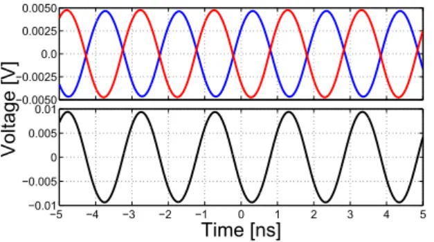
Fig. 9. Mixer IF response, red curve: Channel 1(IF+), blue curve: Channel 2 (IF-), black curve: difference between the two channels
t [1ns/div] V ol t [ 2 m V /d iv]
Fig. 10. Mixer IF response, differential signal showed with a video persistence of 20 seconds and averaging curve of 1 sample.
converts the RF and the LO signal in the differential inputs of the mixer. Figure 9 shows the down-converted response of the mixer. The measure is performed by a LeCroy SDA 813ZI oscilloscope with an averaging of 1000 samples to minimize the noise floor. The extracted phase difference between the two channel is 10 and the amplitude difference is only 0.21 dB. Figure 10 shows the behaviour of the output signal with a persistence of 20 seconds to demonstrate the stability of the measurements.
V. CONCLUSION
This paper shows the design and the performance of a balun for 60GHz applications. The measurement confirms the excellent behaviour predicted by simulations. The balun shows very limited loss better than the state of the art for 60GHz applications [3] (Table 1). Concerning balun dimensions it is the smallest device found in literature with only 0.011 mm2, 80×139µm comprehensive of free space around the coils. The good performance of the balun in an active device have been demonstrated by the use in a fully balanced down conversion mixer.
REFERENCES
[1] T. Dickson, M.-A. LaCroix, S. Boret, D. Gloria, R. Beerkens, S.P. Voinigescu, “30-100-GHz inductors and transformers for millimeter-wave (Bi)CMOS integrated circuits,” IEEE Trans. on MTT, vol.53,no.1, pp. 123-133,jan.2005.
[2] Chao-Shiun Wang, Juin-Wei Huang, Kun-Da Chu, Chorng-Kuang Wang, “A 0.13m CMOS fully differential receiver with on-chip baluns for 60GHz broadband wireless communications,”IEEE Custom Integrated
Circuits Conference, CICC, June 2010.
[3] M. Ercoli, M. Kraemer, D Dragomirescu, R. Plana, “An ultra small pas-sive balun for 60 GHz applications in CMOS 65nm technology,”paper
submitted on 8th IEEE International NEWCAS conference, pp 479-482,
Sept 2008.
[4] M. Kraemer, D Dragomirescu, R. Plana, “Accurate Electromagnetic sim-ulation and measurement of millimeter-wave inductors in bulk CMOS technology,”Silicon Monolithic Integrated Circuits in RF Systems (SiRF),
2010 Topical Meeting on , pp. 61-64 Jan. 2010.
[5] M. Kraemer, D Dragomirescu, R. Plana, “On the De-embedding of small value millimeter -wave CMOS inductor measurement,”German
Microwave Conference (GeMiC), Mars. 2010.
[6] Seo Munkyo, B. Jagannathan, J. Pekarik, M.J.W Rodwell, “A 150 GHz
Amplifier With 8 dB Gain and + 6 dBm Psatin Digital 65 nm CMOS
Using Dummy-Prefilled Microstrip Lines ,”IEEE Journal of Solid-State
Circuits, vol. 44 issue 12, pp. 3410-3421, 2009.
[7] M. Ercoli M. Kraemer, D Dragomirescu, R. Plana, “A passive mixer for 60 GHz applications in CMOS 65nm technology,”German Microwave

![[PDF] Tutoriel de Oracle PL/SQL en pdf | cours informatique](data:image/gif;base64,R0lGODlhAQABAIAAAP///wAAACH5BAEAAAAALAAAAAABAAEAAAICRAEAOw==)