Authors : N. D. Nguyen et al.
Use of p- and n-type vapor phase doping and sub-melt laser anneal for
extension junctions in sub-32 nm CMOS technology
N. D. Nguyena, E. Rosseela, S. Takeuchia,b, J.-L. Everaerta, L. Yanga,h, J. Goossensa, A. Moussaa, T. Claryssea,
O. Richarda, H. Bendera, S. Zaimac, A. Sakaid, R. Looa, J.C. Line,g, W. Vandervorsta,f, M. Caymaxa
a IMEC, Kapeldreef 75, B-3001 Leuven, Belgium
b Department of Physics and Astronomy, KU Leuven, B-3001 Leuven, Belgium
c Department of Crystalline Materials Science, Graduate School of Engineering, Nagoya University, Furo-cho, Nagoya, 464-8603, Japan d Department of System Innovation, Graduate School of Engineering Science, Osaka University, 1-3 Machikaneyama-cho, Toyonaka, Osaka 560-8531, Japan
e TSMC, R&D, 8, Li-Hsin 6th Rd., Hsinchu Science-Based Park, Hsinchu, Taiwan f Instituut voor Kern- en Stralingsfysika - IKS, KU Leuven, B-300I Leuven, Belgium
g TSMC assignee at IMEC, Kapeldreef 75, B-300I Leuven, Belgium
h Department of Chemistry and INPAC Institute, KU Leuven, B-300I Leuven, Belgium
ABSTRACT
We evaluated the combination of vapor phase doping and sub-melt laser anneal as a novel doping strategy for the fabrication of source and drain extension junctions in sub-32 nm CMOS technology, aiming at both planar and non-planar device applications. High quality ultra shallow junctions with abrupt profiles in Si substrates were demonstrated on 300 mm Si substrates. The excellent results obtained for the sheet resistance and the junction depth with boron allowed us to fulfill the requirements for the 32 nm as well as for the 22 nm technology nodes in the PMOS case by choosing appropriate laser anneal conditions. For instance, using 3 laser scans at 1300 °C, we measured an active dopant concentration of about 2.1 × 1020cm-3 and a junction depth of 12 nm. With arsenic
for NMOS, ultra shallow junctions were achieved as well. However, as also seen for other junction fabrication schemes, low dopant activation level and active dose (in the range of 1-4 × 1013cm-2) were observed although
dopant concentration versus depth profiles indicate that the dopant atoms were properly driven into the substrate during the anneal step. The electrical deactivation of a large part of the in-diffused dopants was responsible for the high sheet resistance values.
Keywords : Vapor phase doping ; Atomic layer epitaxy ; Laser anneal ; Ultra shallow junction ; Heavy doping ;
Conformal doping ; Electrical activation
1. Introduction
The development of advanced CMOS technologies requires a continual shrinking of the devices as described by the International Technology Roadmap for Semiconductors [1]. In this down-scaling process, the limits of manufacturability are being stretched in order to meet the increasing demands in efficiency, reliability and accuracy. One of the important requirements for the increase of the performances of MOSFETs in ultra large scale integration is the aggressive scaling of the source and drain extension junctions. Aiming at sub-10 nm junction depths, the achievement of low enough sheet resistance becomes however a progressively more difficult task. Using classical beamline techniques, the junction quality can be degraded by non-trivial issues related to implantation damage when amorphizing species are used to minimize dopant channeling. In the case of non-planar devices such as FinFETs, the requirement of doping conformality poses additional challenges that cannot be addressed by beamline ion implantation (BII) which suffers from shadowing effect for patterns with a high fin density [2]. There is thus a strong need for novel doping strategies both for planar and non-planar devices. Vapor phase doping (VPD) [3] and plasma immersion ion implantation (P3I) [4,5] have already shown
promising results and are potential alternatives to the classical BII. Sub-melt millisecond anneal is considered as the method of choice for dopant activation whereas classical spike rapid thermal annealing (RTA) results in excessive dopant diffusion and limited electrical activation [6,7]. In this work, we investigated the properties of ultra shallow junctions (USJs) fabricated by the combination of VPD and sub-melt laser annealing (LA) and
Authors : N. D. Nguyen et al.
compared them with those obtained by BII using similar LA conditions.
2. Experimental
Boron or arsenic was deposited on 300 mm Si (001) blanket wafers, using a standard horizontal cold wall, load-locked, ASM Epsilon 3200 reactor, a reduced pressure chemical vapor deposition system designed for Si and SiGe epitaxy. Before deposition, the wafers received a NH4OH/O3-based clean followed by an in-situ bake at
1050 °C for 60 seconds in H2 in order to remove the native oxide.
Boron-VPD was performed at 500 °C and reduced pressure using B2H6 (1% in H2) and N2 as carrier gas. For
n-type dopant deposition, AsH3 (0.1% in H2) was used as precursor gas. Typical exposure time of the wafer to the
dopant flow ranges from 1 min to 30 min. Additional details of the VPD process can be found in Refs. [3] and [8]. The activation and the drive-in of the dopants were performed in a N2 ambient using an 808 nm diode bar
laser system from Applied Materials. For all measurements reported in this paper, a fixed scan speed of 150 mm/s was used corresponding to a dwell time of -0.5 ms and the peak wafer temperature was monitored during each scan with an integrated pyrometer. Wafer sheet resistance Rs was determined either by a four-point-probe
Rs100 from KLA-Tencor or by RsL, a non contact measurement technique, using an RsL100 from FSM. Secondary ion mass spectrometry (SIMS) was used to determine the dopant concentrations as function of depth.
3. Results and discussion
3.1. PMOS with boron doping
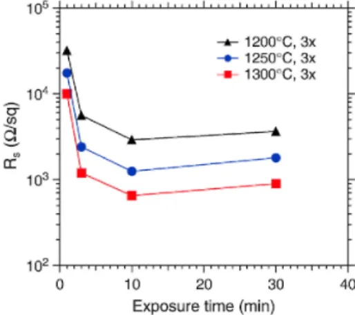
Fig. 1 shows the sheet resistance after 3 LA scans as function of exposure time to the precursor gas. Since the incorporated boron dose increases with time [3,9], the amount of B atoms that can be activated also increases, leading to lower Rs. A minimal value does however exist, due to the incorporated concentration limit set by the
temperature-dependent solid solubility of the dopant. With a laser temperature of 1300 °C, an optimal Rs value of
~600Ω/sq was achieved for 10 min exposure time.
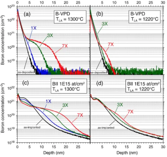
The boron concentration as a function of depth for an as-deposited wafer and the profiles corresponding to wafers that received one or several laser scans, as measured by SIMS, are shown in Fig. 2(a) and (b) for LA temperature of 1300 °C and 1220 °C, respectively. For comparison, the chemical boron concentration profile of an implanted material (0.5 keV, 1 × 1015 cm-2) after similar LA conditions is given in Fig. 2(c) and (d) [10]. When
the number of laser scans increases, the dopant is further driven into the substrate, leading to lower Rs, as shown
in Fig. 3. In the case of VPD and 3 LA scans at 1300 °C, a junction depth xj~12 nm (defined at a concentration of
5 × 1018 cm-3) and an activation level of -2.1 × 1020 cm-3 were obtained together with the R
s value mentioned here
above. The activation level was estimated from the SIMS depth profile by integrating the dopant concentration under a cutoff value. The latter one defines the activation level when the active dose obtained from the integration corresponds to the Rs value, using an iterative procedure [11]. Under similar anneal conditions, the
activation level of the junction fabricated from BII is ~2.3 × 1020 cm-3 with R
s~320 Ω/sq and xj~24 nm. With
B-VPD and 3 LA scans at 1220 °C, xj reduces to ~7 nm with Rs of 1612 Ω/sq.
Fig. 1. Sheet resistance Rs as function of the exposure time to B2H6 for LA temperature of 1300 °C, 1250 °C and 1200 °C, using 3 LA scans.
Authors : N. D. Nguyen et al.
Fig. 2. Depth profiles of the chemical boron concentration by SIMS for (a) VPD and LA at 1300 °C, (b)
B-VPD and LA at 1220 °C, (c) BII 0.5 keV and LA at 1300 °C and (d) BII 0.5 keV and LA at 1220 °C. In each case, the as-deposited or as-implanted profile is plotted with profiles corresponding to one (1×) or more than one (3×, 7×) laser scans.
Authors : N. D. Nguyen et al.
Fig. 4. TEM image of a B-VPD structure after LA at 1300 °C (3 laser scans).
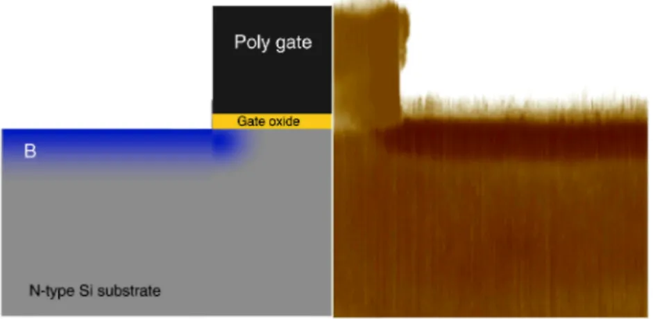
Fig. 5. SSRM image of a cross section around the poly-gate of a patterned wafer. A layout of the structure is
given on the left hand side. The dark regions on the right hand side represent conductive parts of the sample.
The use of VPD clearly results in a sharper as-deposited dopant profile and shallower junctions with a strongly reduced diffusion tail after anneal (Fig. 2). Transmission electron microscope (TEM) inspection did not show any degradation of the crystallinity of the Si substrate after B-VPD and LA at 1300 °C, as shown in Fig. 4. For multiple gate transistor applications such as FinFETs, an equal overlapping of the dopant under all gates is required to guarantee homogeneous device operation. In order to investigate the lateral component of the diffusion, the B-VPD process was applied to a wafer which was prepared with a gate deposition and patterning. Fig. 5 shows a two-dimensional mapping of the cross-section by scanning spreading resistance microscopy (SSRM) where the dark regions denote conductive parts of the structure. This result indicates that boron diffused in an isotropic way during laser anneal, leading subsequently to an effective overlapping of the dopant
concentration under the gate stack.
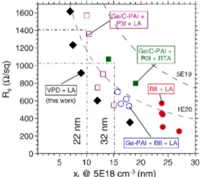
The combination of VPD and LA thus enables the achievement of high quality USJs with abrupt dopant profile and high activation level which are suitable for both planar and non-planar devices. It fulfills the Rs-xj
requirements for the 32 nm and 22 nm technology nodes, as shown in Fig. 6.
3.2. NMOS with arsenic doping
Authors : N. D. Nguyen et al.
behavior of As-VPD leads to the saturation of the adsorbed dose at one atomic layer [8]. In order to avoid dopant desorption during anneal, the As-covered surface was protected by an oxide cap layer deposited ex-situ [14] before LA.
The sheet resistance of As-VPD wafers as function of the LA temperature is shown in Fig. 7. At the LA temperature of 1300 °C, an average Rs value of 1750 Ω/sq was obtained with 10 min of exposure and 3 laser
scans. The decreasing of Rs when the anneal temperature increases results from the combined effect of a higher
activation level and a deeper junction for higher temperatures. The difference between the Rs data for the two
exposure times suggest that the surface saturation by As atoms was not complete after 3 min at the deposition temperature of 600 °C, although we previously showed that an As dose corresponding to 1 atomic layer can be obtained on Si surface after that duration [8]. This can be explained partially by the loss of dopants during LA through the oxide cap which does not act as a perfect sealing of the surface.
In Fig. 8, the chemical As concentration in the as-deposited wafer and in the laser-annealed wafers is plotted as function of depth; exposure time to AsH3 was 3 min. The As peak position was used to define the origin of the
depth scale. The junction depth increases with the anneal temperature and a value of xj~9 nm was achieved using
3 LA scans at 1300 °C. The associated sheet resistance was Rs~3600 Ω/sq. Recently, junctions with Rs~600 Ω/sq
and xj~15 nm using BII and LA were reported [13]. Although SIMS measurements show that As atoms are
effectively driven into Si during LA (Fig. 8), the relatively high value of Rs for the As-VPD process indicates that
only a small part of the dopant concentration is electrically active.
This is confirmed by the determination of the activation level using a procedure similar to that explained in Section 3.1 for B-VPD. The results of the calculations are given in Fig. 9, which shows a comparison between three different processes : VPD with LA at 1300 °C (3×), VPD with RTA at 1050 °C and a reference BII with RTA at 1035 °C. The activation level for As-VPD followed by LA at 1300 °C was about 1.85 × 1019 cm-3. This
value increased to 5 × 1019 cm-3 if RTA was used instead of LA and is consistent with the lower R
s of about 2200
Ω/sq for a similar junction depth (10.5 nm). Although significantly lower Rs (~650 Ω/sq) was measured for the
reference BII process, the related activation level of 5.6 × 1019 cm-3 is comparable to that of VPD combined with
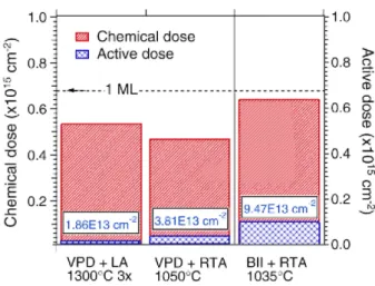
RTA. The depth of the reference implanted junction after RTA was 18.7 nm. As shown in Fig. 10, the active dose values obtained for As-VPD, 1.86 × 1013 cm-2 and 3.81 × 1013 cm-2, respectively with LA and RTA, also confirm
the weak activation of the indiffused As atoms.
Although poor electrical activation of arsenic was also observed for other junction fabrication schemes, the physical root cause in the case of our As-VPD process is still unclear. On the one hand, average carrier mobility in the As-VPD structures, as determined by Hall measurements using a classical Van der Pauw configuration, is in line with the values reported for highly-doped n-type Si [15] and no extended defect could be detected by TEM (Fig. 11). On the other hand, deactivation of As during anneal through the formation of electrically inactive complexes such as dopant-vacancy clusters was reported in ion-implanted Si [16,17]. Therefore, our results suggest that the low activation level in junctions made from As-VPD could also be explained by an important electrical deactivation of the in-diffused dopant atoms. However, the exact nature of these inactive species and the microscopic mechanism of their formation have to be clarified.
Fig. 6. Rs as function of xj for USJs fabricated by various techniques [10,12,13], compared to this work. The
dashed lines denote the Rs(xj) functions for box-like dopant profiles with activation levels of 5 × 1019 cm-3 and of
1 × 1020 cm-3. The R
s-xj regions aimed for the 32 nm and the 22 nm technology nodes are indicated as
Authors : N. D. Nguyen et al.
Fig. 7. Rs as function of the LA temperature, for As-VPD with exposure time of 3 min or 10 min and 3 laser scans.
Fig. 8. Depth profiles of the chemical arsenic concentration by SIMS in as-deposited and laser-annealed wafers.
Authors : N. D. Nguyen et al.
Fig. 9. Activation level and sheet resistance of USJs with As doping using VPD (with LA or RTA) and BII with
RTA The corresponding junction depth is labeled for each process condition.
Fig. 10. Chemical dopant dose and active dopant dose of USJs with As using VPD (with LA or RTA) and BII
with RTA The value of the active dose is labeled for each process condition.
Authors : N. D. Nguyen et al.
4. Conclusions
We have shown that the combination of VPD and LA enables the fabrication of high quality, defect-free USJs with abrupt dopant profile. Excellent results were achieved for B-VPD and these allowed us to fulfill the requirements for both the 32 nm and the 22 nm technology nodes by a proper choice of the LA conditions. For instance, using 3 laser scans at 1300 °C, we obtained an active dopant concentration of ~2.1 × 1020 cm-3 and a
junction depth of ~12 nm. Moreover, an isotropic diffusion of the deposited boron as a result of the laser anneal was demonstrated by SSRM, highlighting that VPD and LA enable the fabrication of conformal doping profiles in FinFET devices. In the case of As-VPD, low dopant activation level and active dose (in the range ~1 - 4 × 10¹³
cm-2) were measured both after LA and RTA, although SIMS depth profiles indicate that As atoms are present in
the substrate with a sufficient quantity. Further investigation is needed in order to clarify the origin and the nature of the electrical deactivation of the in-diffused As atoms. As an extension of this work, the combination of n-type VPD with phosphorus (P) and LA is also considered for USJ fabrication; that study is ongoing.
Acknowledgements
This work was partly performed within the Nanotechnology Support Project in Central Japan (Institute for Molecular Science) which is financially supported by the Nanotechnology Network of the Ministry of Education, Culture, Sports, Science and Technology (MEXT) of Japan.
References
[1] ITRS 2008 (http://www.itrs.net).
[2] W. Vandervorst, P. Eyben, J. Mody, M. Jurczak, N.D. Nguyen, S. Takeuchi, F. Leys, R Loo, M. Caymax, J.-L. Everaert, Proceedings of the 17th International Conference in Ion Implantation Technology, AIP Conf. Proc, vol. 1066, 2008, p. 449.
[3] N.D. Nguyen, F. Leys, S. Takeuchi, R Loo, M. Caymax, P. Eyben, W. Vandervorst, The 4th International SiGe Technology and Device Meeting, Technical Digest, 2008, p. 229.
[4] S.R Walther, N. Variam, S. Norasethekul, J. Weeman, S. Mehta, Proceedings of the 14th International Conference on Ion Implantation Technology, 2002, p. 103.
[5] C. Ortolland, N. Horiguchi, C. Kerner, T. Chiarella, P. Eyben, J.-L Everaert, J.I. Agua Borniquel, T. Poon, K. Santhanam, P. Porshnev, MA Foad, R Schreutelkamp, P.P. Absil, W. Vandervorst, S.B. Felch, T. Hoffmann, Proceedings of the 17th International Conference on Ion
Implantation Technology, AIP Conf. Proc, vol. 1066, 2008, p. 465.
Authors : N. D. Nguyen et al.
Leverd, H. Bernard, S. Warrick, D. Delille, K. Romanjek, R. Gwoziecki, N. Planes, S. Vadot, I. Pouilloux, F. Arnaud, F. Boeuf, T. Skotnicki, International Electron Devices Meeting 2005, IEDM Technical Digest, 2005, p. 679.
[7] T. Noda, W. Vandervorst, S. Felch, V. Parihar, C. Vrancken, S. Severi, A. Falepin, T. Janssens, H. Bender, H. Van Daele, P. Eyben, M. Niwa, R. Schreutelkamp, F. Nouri, P.P. Absil, M. Jurczak, K. De Meyer, S. Biesemans, International Electron Devices Meeting 2006, IEDM Technical Digest 2006, p. 377.
[8] S. Takeuchi, N.D. Nguyen, F. Leys, R. Loo, T. Conard, W. Vandervorst, M. Caymax, ECS Trans. 16 (2008) 495. [9] J. Murota, M. Sakuraba, B. Tillack, Jpn. J. Appl. Phys. 45 (2006) 6767.
[10] E. Rosseel, W. Vandervorst, T. Clarysse, J. Goossens, A. Moussa, R. Lin, D.H. Petersen, P.F. Nielsen, O. Hansen, N.S. Bennett, N.E.B. Cowern, Proceedings of 16th IEEE International Conference on Advanced Thermal Processing of Semiconductors, 2008, p. 135. [11] T. Clarysse, J. Bogdanowicz, J. Goossens, A. Moussa, E. Rosseel, W. Vandervorst, D.H. Petersen, R Lin, P.F. Nielsen, O. Hansen, G. Merldin, N.S. Bennett, N.E.B. Cowern, Material Science and Engineering B 154-155 (2008) 24.
[12] G. Zschatzsch, W. Vandervorst, T. Hoffmann, J. Goossens, J.-L. Everaert, J.I. del Agua Borniquel, T. Poon, Proceedings of the 17th
International Conference on Ion Implantation Technology, AIP Conf, Proc. 1066 (2008) 461.
[13] C. Ortolland, T. Noda, T. Chiarella, S. Kubicek, C Kerner, W. Vandervorst, A Opdebeeck, C. Vrancken, N. Horiguchi, M. de Potter de ten Broeck, M. Aoulaiche, E. Rosseel, S. Felch, P. Absil, R. Schreutelkamp, S. Biesemans, T. Hoffmann, Symposium on VLSI Technology. Digest of Technical Papers, 2008, p. 186.
[14] J.-L. Everaert, G. Zschatzsch, G. Vecchio, W. Vandervorst, L. Cunnane, Proceedings of 16th IEEE International Conference on Advanced
Thermal Processing of Semiconductors, 2008, p. 113. [15] D.B.M. Klaassen, Solid-state Electron. 35 (1992) 953.
[16] P.M. Rousseau, P.B. Griffin, W.T. Fang, J.D. Plummer, J. Appl. Phys. 84 (1998) 3593.
[17] D. Giubertoni, G. Pepponi, S. Gennaro, M. Bersani, M.A. Sahiner, S.P. Kelty, R Doherty, M.A. Foad, M. Kah, K.J. Kirkby, J.C. Woicik, P. Pianetta, J. Appl. Phys. 104 (2008) 103716.