HAL Id: hal-00661491
https://hal.archives-ouvertes.fr/hal-00661491
Submitted on 20 Feb 2018
HAL is a multi-disciplinary open access
archive for the deposit and dissemination of sci-entific research documents, whether they are pub-lished or not. The documents may come from teaching and research institutions in France or abroad, or from public or private research centers.
L’archive ouverte pluridisciplinaire HAL, est destinée au dépôt et à la diffusion de documents scientifiques de niveau recherche, publiés ou non, émanant des établissements d’enseignement et de recherche français ou étrangers, des laboratoires publics ou privés.
Simulation and design of junction termination structures
for diamond Schottky diodes
Fabien Thion, Karine Isoird, Dominique Planson, Marie-Laure Locatelli, Hui
Ding
To cite this version:
Fabien Thion, Karine Isoird, Dominique Planson, Marie-Laure Locatelli, Hui Ding. Simulation and de-sign of junction termination structures for diamond Schottky diodes. Diamond and Related Materials, Elsevier, 2011, 20 (5-6), pp.729-732. �10.1016/j.diamond.2011.03.011�. �hal-00661491�
Simulation and design of junction termination structures for diamond Schottky diodes Authors & affiliations:
F.Thion1,2,3, K.Isoird1,2,D.Planson3, M-L.Locatelli4,5, H.Ding1,2 1CNRS ; LAAS ; 7 avenue du colonel Roche, F-31077 Toulouse, France 2Université de Toulouse ; UPS, INSA, INP, ISAE ; LAAS ; F-31077 Toulouse, France
3Université de Lyon, INSA de Lyon, CNRS UMR 5005, Laboratoire AMPERE, F-69621 Villeurbanne, France 4Université de Toulouse; UPS, INPT ; LAPLACE (Laboratoire Plasma et Conversion d'Energie) ; 118 route de Narbonne,
F-31062 Toulouse cedex 9, France
5CNRS; LAPLACE; F-31062 Toulouse, France.
Abstract: In this paper, the first step of the design of a junction termination structure usable on diamond Schottky diodes is
introduced. Through the collaboration of AMPERE and LAAS laboratories, a study of junction termination structures using field plates and semi-resistive materials was carried out. Several results from simulations of P type Schottky diodes protected by MESA coated with several layers of dielectric materials are shown in this paper. The analysis of those simulations, conducted on pseudo-vertical diodes protected by a field plate on a semi-resistive layer deposited on top of a dielectric, shows a great efficiency of such junction termination structures.
I. Introduction:
Diamond is well known for being an exceptional material. It has one of the best thermal conductivity and is amongst the toughest. It is also a promising candidate for power electronics, seeing its numerous theoretical qualities. As a wide band-gap semiconductor [1], [2], it is expected to be the material best suited for working under extreme conditions [3], [4]. The first unipolar diodes made on diamond start to appear in laboratories. They are elaborated on homo-epitaxied and in-situ doped substrates.
All power electronics components need a junction termination structure to limit the peripheral electric field. The particular properties of diamond (like permittivity, band gap, critical electric field) imply an adaptation of this structure.
With those first batches of components, we need to develop junction termination structures that will allow the diamond components to reach their full potential, mainly in terms of breakdown voltage. Since diamond has a huge theoretical critical electric field, the junction termination structure is going to have a major impact on the performance of the components. Those structures will allow us to demonstrate the efficiency of such diamond components.
II. Simulation platform:
The simulation platform has been implemented using TCAD SENTAURUS, a finite elements calculus software. We have worked with models already implemented in the software, such as the ones used for silicon or for silicon carbide, tuning them to the diamond properties. The latter values are taken from a large bibliographic study (for instance [6], [7]). However, it is reasonable to mention the fact that some values collected throughout the bibliographic study are extrapolated from other semiconductors, or underestimate its theoretical capabilities, mostly because of the poor quality of the samples on which the different studies were carried out. Nevertheless, the parameter file is regularly updated with the latest experimental results.
III. Junction termination structure: A: Introduction
The peripheral protection is a structure implemented during the process and is part of the design. This device is developed to reach the theoretical breakdown voltage (equivalent to the breakdown voltage of a plane parallel infinite junction), by spreading out the equipotentials at the junction periphery, hence avoiding local increases in the electric field which can lead to premature breakdown voltage. The efficiency of a peripheral junction protection is evaluated using the percentage of the theoretical breakdown voltage.
Some steps of the process, like ion implant in diamond, are yet to be perfected and do not allow the use of standard peripheral protections, like guard rings or JTE (Junction Termination Extension). We then need to imagine peripheral protections based upon etching and layers of dielectrics and metals, such as the field plate protection technique as described in [8].
Using a layer of semi-resistive material is an alternative technique to minimize local increases of the electric field in the surface dielectric layer at the edge of the metallic contact. Since diamond electronic devices are intended to work at high temperatures, it seems interesting to study the behavior of semi-resistive materials used as field plate protections. Indeed, resistivity decreases in a lot of dielectrics when the temperature rises.
B: Field plate on a dielectric material
Fig 1: Simulated pseudo-vertical structure. The question marks symbolize the parameters which are studied.
The simulated structure is introduced in Fig.1. To make this pseudo-vertical structure, the Schottky contact is deposited on top of the P- layer, doped at 8.1015 cm-3 and 7 µm thick. To get to the P+ layer (doped at 3.1020 cm-3 and 5 µm thick) and further
deposit the Ohmic contact, the P- layer is etched. One or several layers of dielectric materials and a field plate are what make this peripheral protection. First, we studied the field plate with only one dielectric material. Then, we tested the result of the combination of a semi-resistive layer deposited on the chosen dielectric. The theoretical breakdown voltage of such a structure is 1500V at 600K. This breakdown voltage reaches 1990V at 800K. Taking into account an efficiency of 80% for the peripheral protection, we should reach the breakdown voltage of 1200V at 600K for the real structure.
A field plate is defined by two main parameters: the thickness of the dielectric and the length of the field plate.
First, the dielectric used in the simulations is chosen between SiO2 and Si3N4, which are both available in the clean room of
the laboratory. Simulations show that the bigger the permittivity is, the better is the breakdown voltage, as shown in Fig. 2.
Fig 2 a) and b):3D views of the simulations of the diamond diode reverse characteristics protected by a field plate on two different dielectric materials. SiO2 is used on Fig 2.a) and Si3N4 is used on Fig 2.b).
Fig 2. shows that the best breakdown voltage is obtained for field plates on Si3N4. We notice that the behavior is similar with
both dielectrics: the thickness allows obtaining a critical value for the breakdown voltage and the field plate length provokes a saturation of the breakdown voltage for its higher values.
Fig 3. shows how the electric field spreads across the AA’ axis of the structure. We notice two maximums: one at the edge of the Schottky contact and one at the edge of the field plate.
The best configuration is obtained when the two maxima have the same value, which is when the field plate is 10µm long. Hence, the maximum breakdown voltage is 1720V (84% efficiency) for a Si3N4 layer with a thickness of 900nm and a field plate of
10µm.
Fig 4: Equipotential lines in the structure at breakdown voltage (around 1.7kV as shown above). The thickness of Si3N4 is 900nm and the field plate is 10µm long.
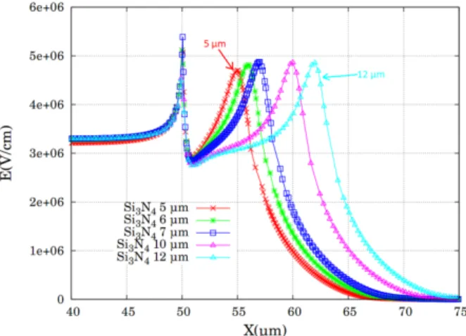
Fig 5: Electric field in the Si3N4 at the interface of the nitride and the field plate for field plate length between 5 µm and 18 µm.
Fig 4 and 5 show respectively the equipotentials in the structure and the electric field in the silicon nitride at the interface of the nitride and the field plate while at breakdown voltage. It shows that in diamond, the edge of the Schottky contact is where the breakdown occurs and that the value of the electric field is twice as much as its value in diamond (see Fig .3), risking a rupture of the dielectric. Hence using a semi-resistive material may help the device behave closer to the theoretical one.
C: Field plate on a semi-resistive deposited on a layer of dielectric
The simulated structure is the same, with an added layer of a semi-resistive material on a layer of Si3N4. Simulations show
that the thickness of the semi-resistive layer does not influence the breakdown voltage: only its resistivity changes the level of leakage currents. The resistivity of a typical semi-resistive material is between 107 and 1012 Ω.cm, depending mostly on the
temperature.
The main parameters used to tune the breakdown voltage of the structure are the thickness of the nitride, the thickness of the semi-resistive layer, the resistivity of the semi-resistive layer and the length of the field plate.
Thus, the breakdown voltage is tuned using the same method as previously with the same two parameters: field plate length and Si3N4 thickness.
Fig 6: Equipotentials in the structure protected by a semi-resistive layer on top of a dielectric
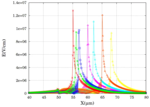
Fig 7: a) 3D view of the simulations of diamond diodes reverse characteristics protected by a field plate on a semi-resistive layer deposited on a Si3N4 layer. In blue the maximum value and in red the minimum value. b) Value of the electric field at breakdown voltage on the AA’ axis (top curves) and on the top edge of the nitride
(bottom curves)
Results show that the maximum breakdown voltage obtained is 1830V, for an efficiency of 92%, with a thickness of 540nm and a field plate length between 5 and 10 µm. Equipotentials are spread out along the whole semi-resistive layer (Fig.6), which contributes to avoid the breakdown to occur at the edge of the field plate and instead puts it at the side of the P- layer, where the equipotentials tighten. What’s more, in Fig.7 b), we notice that the value of the electric field is more than twice less in the nitride layer. By moving the position of the electrode of the Ohmic contact, we can “choose” where the breakdown is going to happen, hence being able to deduce where the device is the most fragile.
D. Conclusion and perspectives
The peripheral junction protection based upon a combination of semi-resistive material resting upon a layer of silicon nitride seems to give promising results. The efficiencies simulations return are respectively of 84% for a field plate on silicon nitride and of 92% with the help of a semi-resistive material. Optimizations can still be made on those designs. Hence extensive studies of diamond etching process and of the behavior of semi-resistive materials with temperature have to be carried out. New optimized devices will be realized in the near future.
References:
[1] M.Nesladek, “Conventional n-type doping in diamond: state of the art and recent progress,” Semiconductor Science and Technology,|2005|.
[2] J.E.Butler, M.W.Geis, K.E.Krohn, J.Lawless, S.Deneault, T.M.Lyszczarz, D.Flechtner and R.Wright, “Exceptionally high voltage schottky diamond diodes and low boron doping,” Semiconductor Science and Technology, vol.18, no.3, pp.S67–S71,|2003|.
[3] C.Raynaud, D.Tournier, H.Morel and D.Planson, “Comparison of high voltage and high temperature performances of wide bandgap semiconductors for vertical power devices,” Diamond and Related Materials, vol.19, pp.1–6,2010.
[4] K.Shenai, R.Scott and B.Baliga, “Optimum semiconductors for high-power electronics,” IEEE, p.1811, 1989. [5] Sentaurus user guide A-2008.09.
[6] S.Rashid, A.Tajani, D.Twitchen, L.Coulbeck, F.Udrea, T.Butler, N.Rupesinghe, M.Brezeanu, J.Isberg, A.Garraway, M.Dixon, R.S.Balmer, D.Chamund, P.Taylor and G.A.J.Amaratunga, “Numerical parameterization of chemical-vapor-deposited single-crystal diamond for device simulation and analysis,”|2008|.
[7] T.Teraji, H.Wada, M.Yamamoto, K.Arima and T.Ito, “Highly efficient doping of boron into high quality homoepitaxial diamond films,” Diamond and Related Materials, vol.15, no.4-8,pp.602–606,|2006|.
[8] M.Brezeanu, M.Avram, S.Rashid, G.A.J.Amaratunga, J.E.Butler, N.Rupesinghe, F.Udrea, A.Tajani, M.Dixon, D.Twitchen, A.Garraway, D.Chamund, M.J.Taylor and G.Brezeanu, “Termination structures for diamond schottky barrier diodes,” Proceedings of the 18th International Symposium on power semiconductor devices and IC’s,|2006|.