HAL Id: hal-00722641
https://hal.archives-ouvertes.fr/hal-00722641
Submitted on 2 Aug 2012
HAL is a multi-disciplinary open access
archive for the deposit and dissemination of
sci-entific research documents, whether they are
pub-lished or not. The documents may come from
teaching and research institutions in France or
abroad, or from public or private research centers.
L’archive ouverte pluridisciplinaire HAL, est
destinée au dépôt et à la diffusion de documents
scientifiques de niveau recherche, publiés ou non,
émanant des établissements d’enseignement et de
recherche français ou étrangers, des laboratoires
publics ou privés.
Transient Voltage Overshoots of High Voltage ESD
Protections Based on Bipolar Transistors in Smart
Power Technology
Antoine Delmas, Amaury Gendron, Marise Bafleur, Nicolas Nolhier, Chai Gill
To cite this version:
Antoine Delmas, Amaury Gendron, Marise Bafleur, Nicolas Nolhier, Chai Gill. Transient Voltage
Overshoots of High Voltage ESD Protections Based on Bipolar Transistors in Smart Power Technology.
Bipolar/BiCMOS Circuits and Technology Meeting (BCTM), Oct 2010, AUSTIN, United States.
pp.253-256. �hal-00722641�
Transient Voltage Overshoots of High Voltage ESD
Protections Based on Bipolar Transistors in Smart Power
Technology
A. Delmas
1,3,4, A. Gendron
2, M. Bafleur
3,4, N. Nolhier
3,4and C. Gill
21
Freescale Semiconducteur, 134 Av. du General Eisenhower, 31023 TOULOUSE Cedex, FRANCE
2Freescale Semiconductor, 2100 E. Elliot Road, TEMPE AZ 85284, USA
3
CNRS; LAAS; 7 Avenue du Colonel Roche, F-31077 TOULOUSE, FRANCE
4
Université de Toulouse; UPS, INSA, INP, ISAE, LAAS, F31077 TOULOUSE, FRANCE
Abstract — Transient voltage overshoots of a high
voltage (20 V) ESD clamp based on bipolar transistors in a smart power technology are studied using different TLP pulse conditions (rise time, voltage amplitude). The physical mechanisms involved during the ESD clamp turn-on are thoroughly analyzed by the mean of TCAD simulations, allowing the definition of a set of design guidelines for the overshoot reduction.
Index Terms — Electrostatic discharges (ESD),
device physics, bipolar simulation, smart power technologies.
I. INTRODUCTION
Efficiently protecting smart power technologies against ESD is particularly challenging for two main reasons: the need to clamp the discharge current under high voltages and the narrowing of the ESD design window [1]. To overcome the first issue, efficient protection devices are bipolar-based ones that allow the power dissipation within the semiconductor volume. Regarding the ESD design window, it is defined on the lower limit by the supply voltage of the integrated circuit and on the upper limit by the breakdown voltage (generally the gate oxide one) of the device to be protected. Typically, ESD designers rely on TLP characteristics to check if their protection is fitting in the design window. However, such characteristics are quasi-static and do not capture fast voltage transients, which can be harmful for the device to be protected [2].
A major drawback of bipolar devices in smart power technologies is their dynamic response that can induce voltage overshoot upon the ESD stress. The physical mechanisms inducing this overshoot have to be thoroughly characterized and understood both to take it into account the ESD design window and to improve the dynamic performance of the protection device.
In the following, section II presents the technology and the protection device under study. Section III provides measurement results of the overshoot behavior under various types of TLP pulses. Section IV analyzes the device behavior during the overshoot and proposes design guidelines to minimize it.
II.ESD PROTECTION DEVICE
This study is carried out for an ESD clamp targeting the protection of 20 Volts I/Os in a 0.25 µm smart power technology featuring a low-doped P--epitaxy, a
high-doped P+-substrate, a high-doped N+-buried layer
and deep trench isolation.
A. Device description
The device is an implementation of bipolar transistors providing a protection against positive and negative ESD (Fig. 1). It is formed by two P-wells isolated from each other by a deep N-well connected to an N+-buried layer (NBL). Shallow highly-doped N
and P-type diffusions are located in each P-well. The whole device is surrounded by a N-well isolation ring.
Fig. 1. Simplified cross-section of the 20 V ESD clamp under test.
In this study, we will only consider a positive ESD event. Given this condition, three bipolar transistors have to be taken into account: a lateral NPN having the P-well tied to the ground as the base, the shallow N diffusion in this P-well as the emitter and the middle N-well as the collector, a vertical NPN having the same emitter and base as the lateral NPN but the NBL as the collector and a lateral PNP having the base and collector of the lateral NPN as respectively its collector and base and the P-well tied to the signal as the emitter.
The triggering of the protection relies on the self-biasing effect in the lateral NPN transistor. Basically,
P -P+ N+ Oxide P -Oxide P++ Oxide N++ Oxide P++ P N- P N++ N N N N++ Sp ESD 253 978-1-4244-8579-6/10/$26.00 ©2010 IEEE
when the voltage reaches the avalanche breakdown of the reverse biased base/collector junction (N-well/P-well junction), holes are injected into the base and progressively build up a potential drop across the emitter/base junction. Eventually, the transistor turns-on, and the voltage drops as the electrons injected by the emitter contributes to the avalanche. Concurrently, the vertical NPN gets also triggered as it shares its emitter-base junction with the lateral NPN. The triggering voltage (Vt1), which is closely related to the
avalanche breakdown voltage, can be properly adjusted through the spacing (Sp) between N-well and P-well masks.
The lateral NPN turning-on tends to induce a SCR effect by biasing the lateral PNP. However, high current densities are required to get the full SCR effect. At low current, the bipolar gain of the PNP is too low (lower doping concentration for P-well than N-well) to provide an effective feedback. Such behavior allows leveraging the SCR to get a low on-state resistance (RON) and a high robustness, while
keeping a high holding voltage (VH).
B. TLP Characterization
Quasi-static transmission line pulse (TLP) measurements (100 ns pulse width, 10 ns rise time) were performed on 75mm-long devices (Fig. 2). The results exhibit a Vt1 of 28.9 V and a VH of 12.5 V.
The device gets damaged for a current (It2) of 6.9 A,
corresponding to an increase of the leakage current.
Fig. 2. TLP characteristic of 20 V ESD clamp.
III.TRANSIENT VOLTAGE OVERSHOOT
CHARACTERIZATION A. Description of the measurement set-up
A dedicated experimental setup has been developed by the authors [3] to provide a precise characterization of the transient behavior of ESD protections. This “transient TLP” (t-TLP) tool is based on a modified 50 Ω very fast Transmission Line Pulsing (vf-TLP) measurement setup, for which the frequency response has been characterized and used
as a correction function for scope raw data. It allows the extraction of V(t) and I(t) characteristics for pulse voltages up to 1000 V and pulse widths from 1.25 to 100 ns. The time resolution is 60 ps and the voltage error less than 4 V. Even though the purpose of the t-TLP tool development was to characterize the overshoot of the ESD protections, it can also be used as a precise “quasi-static” TLP/vf-TLP tester, by averaging V(t) and I(t) waveforms in the last nanoseconds. Then a set of I-V points is obtained for every TLP pulse voltage, as in the conventional TLP setup.
B. Experimental Results
t-TLP measurements were performed on the 20 V clamp for 1 and 10 ns rise times (tr). For each pulse,
the maximum voltage (VMax) reached by the
protection during the triggering was extracted (Fig. 3). VMax values grow continuously with the current, up to
approximately 37 V at 6 A for 10 ns rise time and 50 V for 1 ns rise time. Compared to Vt1, it corresponds
to, respectively, 8 V and 21 V overvoltages, which have to be taken into account for the design window.
Fig. 3. I-VMax curves with I the quasi-static TLP current for 100 ns pulse width and VMax the peak voltages for both 10 ns and 1 ns rise times. The quasi-static TLP characteristic is plotted as a reference.
IV. ANALYSIS OF THE DEVICE OPERATION DURING
THE OVERSHOOT
A. Time dependent conditions for the voltage snapback
To determine the condition for a device to snapback during a TLP pulse, we will consider the equivalent circuit of the tester presented in Fig. 4. The condition for the voltage to reach its maximum can be written as:
0 =
dt
dVDUT (1)
where VDUT, the voltage across the device, is equal to:
DUT ser gen DUT V R I V = - (2) 254
with, Vgen the TLP source voltage, Rser the series
resistor in the equivalent circuit of the TLP, typically 50 W, and IDUT the current through the device. By
combining equations (1) and (2), we obtain the snapback condition: dt dV dt RI d( DUT ) = gen (3)
This condition means that the increase of the TLP source voltage is compensated by the increase of the voltage drop induced by the DUT current through the TLP resistance. Basically, the measurement set-up impacts the overshoot through both the voltage slope and the series resistance. We can notice that, when the TLP pulse reaches its plateau, the ESD device can easily snap back as dVgen/dt is equals to zero.
However, in this particular case, the overshoot is directly correlated to the shape of the TLP pulse and do not represent the device behavior during a real event (HBM for example).
Gen Rser DUT Vgen VTLP tr t
Fig. 4. Simplified version of a TLP tester equivalent circuit B. TCAD simulations results
In order to investigate the physical behavior of the ESD device during the overshoot, two dimensional device simulations were performed using Synopsys TCAD tools. First, the device doping cross-section was generated by process simulation. Then, a particular care was taken in selecting the physical models required for accurate electro-thermal simulations of ESD devices. As part of this calibration process, the electrons and holes lifetimes were adjusted to fit the bipolar gain at low current, as recommended in [4].
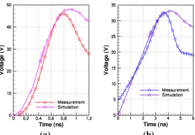
The simulation results for 100 V TLP pulses with 1 ns and 10 ns rise times are presented in Fig. 5. Up to VMax, the agreement with measurements is very good
(the precision on VMax value is 4 % and 1.5 % for 1 ns
and 10 ns rise times, respectively). After snapback, the voltage does not drop as fast in simulation as in measurement. This discrepancy can be attributed to the inaccuracy of the generation model under high current conditions. However, as long as we focus on the physical mechanisms controlling the peak voltage VMax, the simulation study can be used with
confidence to get a deeper insight into the involved phenomena.
(a) (b)
Fig. 5. Measured and simulated voltage waveforms at the beginning of a 100 V TLP pulse for 1 ns (a) and 10 ns (b) rise times.
We can notice the peak voltages are reached before the end of the TLP voltage rise, for t<tr. In these
cases, the overshoot is not impacted by the change in the slope of the TLP pulse when it reaches its plateau.
C. Physical mechanisms controlling the overshoot
In the following of the study, we will focus on the simulated voltage waveform for 10 ns rise time (Fig. 5 b).
The first parameter of interest is the delay for the ESD device to go into snapback after it reaches its DC breakdown voltage (BV), at the time tBV. A static
simulation gave a value of 24.9 V for BV. By reporting it on the voltage waveform, we get a delay of 1.77 ns during which the voltage increases by 8.2 V (Fig. 6).
BV VMax
tBV tM
ax
Fig. 6. Simulated voltage and current waveforms next to the peak voltage.
To start getting insight into the behavior of the ESD device during this delay, we have plotted the emitter and base current waveforms (Fig. 6). The base current starts increasing immediately after time tBV, thanks to
avalanche holes generation, followed after approximately 400 ps by the emitter current, but very slowly at the beginning (it reaches 10 mA with a delay of 630 ps during which the voltage has already increased by 5.2 V). The emitter current gradually builds up, reaching higher values and counteracting more efficiently the TLP voltage increase. When the
device finally snaps back, the emitter current is already relatively high, close to 170 mA.
The delay for the emitter current to set up corresponds to the time required for the avalanche current to bias the emitter-base junction, or, in other words, to charge the emitter-base junction capacitance, as was described in [5]. Based on these observations, a first set of design guidelines can be defined to reduce the overshoot: increasing the P-well resistance (for example by pushing the base contact away from the emitter or adding an external resistance) and reducing the emitter-base junction capacitance (for example by designing a smaller emitter).
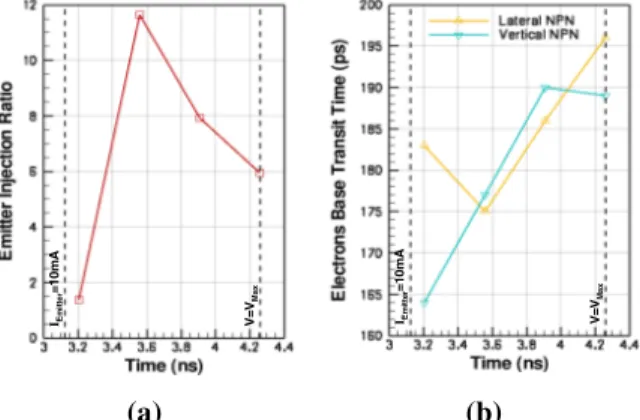
When the emitter-base junction becomes forward biased, the lateral NPN transistor can enter in its self-biased mode. The remaining delay for the device to snap back will depend on how strong the feedback is between the electron current coming from the emitter and the avalanche at the base-collector junction. Under these conditions, the emitter injection ratio (Fig. 7 a) and the electrons base transit time (Fig. 7 b) are critical as they set, respectively, the efficiency of the emitter injection and the time constant of the feedback. The low value of the injection ratio at 3.20 ns means that the emitter-base diode has not been triggered yet and the decreasing trend observed after reaching a maximum value is typical of high current effects. The variations in the values of the base transit time are also related to high current effects.
A second set of design guidelines for the overshoot reduction can be defined targeting an increase of the emitter injection ratio and a decrease of the electrons base transit time. However, such rules have to be applied with care as they will tend to reduce the holding voltage [6]. V =V M ax IEm it te r =1 0m A V =V M ax IEm it te r =1 0m A (a) (b)
Fig. 7. Emitter Injection (a) and electrons base transit times for the lateral and vertical NPN (b).
In addition, Fig. 7 b shows that the base transit times for the lateral and vertical NPN are close to each other. This leads to a split of the base current between the lateral and the vertical paths (Fig. 8). As a result, some of the electrons injected by the emitter do not flow through the high avalanche region located
at the lateral base-collector junction. The vertical NPN, which has a very positive impact on the robustness, turns out to slow down the snapback.
V>0
Fig. 8. Current density distribution at t(V=VMax) showing the lateral and vertical current paths.
V. CONCLUSION
The transient turn-on of a 20 Volts ESD clamp based on bipolar transistors has been characterized by the mean of a home-made transient ESD tester. Voltage overshoots above Vt1 have been reported, up
to approximately 30 % for 10 ns rise time and 70 % for 1 ns rise time. By leveraging TCAD simulations, the overshoot was divided into two segments. The first one corresponds to the time required to forward bias the emitter-base junction, and the second to the gradual increase of the emitter current in a self-biased NPN transistor. Thanks to these results, design guidelines for the overshoot can be defined by targeting: the increase of the P-well resistance, the decrease of the emitter-base junction capacitance, the increase of the emitter injection ratio and the decrease of the electrons base transit time.
REFERENCES
[1] M.P.J. Mergens, M.T. Mayerhofer, J.A. Willemen, M. Stecher, “ESD Protection Considerations in Advanced High-Voltage Technologies for Automotive”, in Proc. EOS/ESD Symposium, pp. 54-63, September 2006.T. [2] T. Smedes, and N. Guitard, “Harmful voltage
overshoots due to turn-on behaviour of ESD protections during fast transient”, in Proc. EOS/ESD Symposium, pp. 357-365, September 2007.
[3] A. Delmas, D. Tremouilles, N. Nolhier, M. Bafleur et al., “Accurate Transient Behavior Measurement of High-Voltage ESD Protections Based on a Very Fast Transmission-Line Pulse System,” in Proc. EOS/ESD Symposium, September 2009.
[4] K. Esmark, “Device Simulation of ESD Protection Elements”, Series in Microelectronics, vol.128, ISBN 3-89649-781-2, 2002.
[5] J. Di Sarro, K. Chatty, R. Gauthier and E. Rosenbaum, “Study of Design Factors Affecting Turn-on Time of Silicon Controlled Rectifiers (SCRs) in 90 and 65 nm Bulk CMOS Technologies,” in Proc. IRPS 2006, pp. 163-168.
[6] A. Gendron, P. Renaud, P. Besse, C. Salamero et al., “Area-Efficient Reduced and No-Snapback PNP-based ESD Protection in Advanced Smart Power Technology,” in Proc. EOS/ESD Symposium, pp. 69-76, September 2006.