HAL Id: hal-01934788
https://hal.archives-ouvertes.fr/hal-01934788
Submitted on 3 Feb 2021HAL is a multi-disciplinary open access archive for the deposit and dissemination of sci-entific research documents, whether they are pub-lished or not. The documents may come from teaching and research institutions in France or abroad, or from public or private research centers.
L’archive ouverte pluridisciplinaire HAL, est destinée au dépôt et à la diffusion de documents scientifiques de niveau recherche, publiés ou non, émanant des établissements d’enseignement et de recherche français ou étrangers, des laboratoires publics ou privés.
Molecular Film
Lorenzo Poggini, Mathieu Gonidec, Juan González-Estefan, Gilles
Pécastaings, Benoît Gobaut, Patrick Rosa
To cite this version:
Lorenzo Poggini, Mathieu Gonidec, Juan González-Estefan, Gilles Pécastaings, Benoît Gobaut, et al.. Vertical Tunnel Junction Embedding a Spin Crossover Molecular Film. Advanced Electronic Materials, Wiley, 2018, 4 (12), 1800204 (8 p.). �10.1002/aelm.201800204�. �hal-01934788�
Vertical Tunnel Junction Embedding a Spin Crossover Molecular Film
Lorenzo Pogginia,b, Mathieu Gonideca,b, Juan H. González‐Estefana,b, Gilles Pecastaings C, Benoît Gobaut d, Patrick Rosaa,b
a
CNRS, ICMCB, UMR 5026, F‐33600 Pessac, France
b
Univ. Bordeaux, ICMCB, UMR 5026, F‐33600 Pessac, France
C
Université de Bordeaux‐INP, LCPO‐CNRS, UMR 5629, F‐33607 Pessac, Cedex, France
d
Synchrotron SOLEIL, L'orme des Merisiers, Saint‐Aubin‐BP48, F‐91192 Gif‐sur‐Yvette, Cedex, France
Corresponding Author : [email protected] / orcid.org/0000-0002-1931-5841 / E‐ mail: [email protected],
Abstract :
Thin films of a molecular spin crossover (SCO) Iron(II) complex featuring a high transition temperature are grown by sublimation in high vacuum on TSAu and investigated by X‐ray and UV photoelectron spectroscopies. Temperature‐dependent studies demonstrate that the thermally induced spin crossover behavior is preserved in thin films. A large‐area ultrathin switchable spin crossover molecular vertical tunnel junction with top electrodes of the liquid eutectic of gallium and indium, for which the spin‐state switching of the films induces a two orders of magnitude change in the tunneling current density flowing through the junction, is reported here. The results on large‐area junctions, rationalized by density functional theory calculations, demonstrate the high potential of SCO‐based switchable molecular junctions as functional devices.Keywords: Eutectic gallium indium alloy (EGaln) ; Spin crossover (SCO) ; Thin films ; Tunnel junctions
1 Introduction
From the technological point of view spin cross‐over (SCO) molecular materials have been proposed for numerous applications ranging from memory devices1 to gas, pressure, and temperature sensors.2, 3
SCO materials are proposed to be good candidates as active components in prospective spintronics and molecule‐based data storage devices4, 5 as well as in innovative devices taking advantages from additional features, combining SCO with other functionalities.6, 7 Considering all those possible applications, the study of the electrical properties of SCO compounds is fundamental, to understand how they behave under electronic stimuli, especially when prepared as thin films.8, 9 Indeed, these molecules can be switched between two electronic states—termed high‐spin (HS) and low‐spin (LS)— with different magnetic, optical, and structural properties by the action of external stimuli (pressure, temperature, light‐irradiation)10-14 making them promising systems for new functional materials.7 This is particularly important since the use of electrical stimuli to control (read/write) the spin‐state of the system would provide a great advantage toward technological applications, compared to other conventional addressing methods such as light irradiation, and changes in temperature or pressure, that are less easily implemented. In this paper, we show that it is possible to design large area switchable molecular tunnel junctions, in which the switchable tunneling barrier is made of a thin film of a SCO compound. Those thin films, made by evaporation on TSAu (template‐stripped gold), were thoroughly characterized using highly‐sensitive and specific surface tools. Electrical switching has been studied as a function of temperature in a tunnel junction configuration, and the experimental results have been rationalized thanks to a theoretical model based on energy levels and electronic densities obtained at density functional theory (DFT) level. The good correlation we establish between experimental measurements and modeling proves the feasibility to design, manipulate, and read such ultrathin film devices, an important prerequisite for the development of future active multistable devices. The most critical issues toward the development of large‐area spin‐crossover based molecular junctions are i) to
obtain high quality SCO thin films over large areas and ii) to have a measurement methodology that allows to measure their properties in an efficient and reliable manner. Moreover, to facilitate further developments and applications of those systems, it is highly desirable to have a transition temperature (and thus, possibly, a switching temperature) close to room temperature. For those reasons, we have
chosen the [Fe(HB(trz)3)2] SCO complex, hereafter called 1 (HB(trz)3 =
tris(1H‐1,2,4‐triazol‐1‐yl)borohydride),15-18 for which it was shown recently that it can be deposited as continuous thin films on surfaces by thermal evaporation.19, 20
Some recent efforts have focused on vertical large area SCO junctions with film thicknesses in the 10– 200 nm range by evaporation of metallic top contacts over molecular films on two closely related SCO complexes.5, 21 This methodology works well for rather thick films (a few tens or hundreds of nm), but for thinner films—of ≈1–5 nm, as may be required to obtain good quality tunnel junctions—it is likely to yield an unacceptably high amount of shorted devices. Altogether, large area junctions incorporating very thin films of those two closely related compounds showed no significant variation of conductance with temperature for 10 and 30 nm films of [Fe(HB(trz)3)2],21 and only a small conductance switching in
the case of 8.1 nm films of [Fe(H2B(pz)2)2(phen)].5 Conversely, the same authors showed that junctions
incorporating thicker films of 100–200 nm of [Fe(HB(trz)3)2], for which charge transport likely occurs in
the hopping regime, exhibited a jump in conductance switching of about one order of magnitude upon spincrossover.21 This may be, in part, due to interpenetration of the molecular thin film and the evaporated top electrode, or (as mentioned by the authors themselves) to mechanical aspects linked to the nature of this sandwich metal–insulator–metal junction. Indeed the sensitivity of SCO compounds to external pressure leading to inhibition of spin state switching is known, and one possible hypothesis would be to think that this should be exacerbated for thin films.22-24
2 Results and Discussion
In the present study, we measured vertical SCO molecular junctions by using a soft conformal EGaIn (for Eutectic Gallium Indium alloy, 75% Ga and 25% In in mass, see schematic representation in Figure 1a) top electrode that specifically addresses the main challenges one can expect to encounter when measuring vertical SCO junctions. In particular, this top electrode provides a soft, deformable top contact which should ensure that the molecular film is intact (i.e., not breached by the top electrode) even at very low thicknesses; it should also provide mechanical compliance of the electrode with the deformation of the molecular film, while ensuring a small footprint which should minimize the occurrence of short‐circuits. This type of soft top electrode has been used by us and others to study molecular tunnel junctions with great efficiency25-29 and has recently been employed to study inorganic complex systems.30-32 In our hands using an EGaIn top electrode afforded tunnel junctions with a two orders of magnitude abrupt change in conductivity at the crossover temperature.
Figure 1 : a) schematic representation of the TSAu//SCO//Ga2O3/EGaIn junction with the structure of 1 represented in the inset
and b) VSM measurement of the purified starting material (black dots) under 10 kOe, and SQUID measurement of a 6 × 90 mm 100 nm thick strip of complex sublimated on Kapton foil (red dots).
2.1 Bulk and Thick Film Magnetic Characterization
Magnetic characterization of the thermally driven SCO in a 100 nm thick film on a Kapton substrate has been carried out with a SQUID magnetometer and compared with a bulk powder sample measured with a vibrating sample magnetometer (VSM) (see Figure 1b).
The measurement on the bulk powder shows a transition temperature T1/2 of 326 K with a small 3 K
hysteresis, in line with the values of T1/2 recorded previously for the dehydrated complex (magnetic
measurement gives 333 K18, 19 and Raman spectroscopy about 325 K18). The 390 K χMT value of 3.08
cm3 K mol−1 is higher than that previously reported, which was slightly below the expected spin‐only value (3.00 cm3 K mol−1), contrary to what is expected for HS Fe(II) (values typically in the range 3.1–3.8 cm3 K mol−1). The microcrystalline powder sample of complex 1 is therefore almost fully high‐spin at 390 K, and becomes almost fully LS at low temperature, reaching a χMT value of 0.1 cm3 K mol−1 at 200 K.
The thin film on Kapton shows a very similar behavior, with an almost fully diamagnetic state at low temperature with a χMT value of 0.14 cm3 K mol−1 at 200 K. The highest temperature that can be
reached with the Kapton tape without damaging it was 350 K, and the spin crossover is still incomplete at that temperature (2.63 cm3 K mol−1 at 350 K), illustrating a slightly more gradual character than in the bulk sample. The observed T1/2 of 333 K is again in line with previously reported measurements for both
hydrated15, 33 and dehydrated complexes, and the thermal hysteresis width (if significant) is reduced to less than 1 K. A comparison between the thermal switching of the pristine powder sample and the sublimated film reveals that the nanostructuration has an effect on the compound, in particular inducing a slightly more gradual SCO transition and increasing the residual LS fraction at high temperatures (incomplete SCO). Recently it has been reported for the very same complex evidence for an increase of the spin crossover temperature by reducing the thickness of films deposited on silica wafer.34 These findings may arise from packing inhomogeneity, similarly to what was previously found for doped SCO systems13, 35 for which the cooperativity was different than that of the pure compound, and may also arise from a relevant increase of surface energies when going from the low‐spin to the high‐spin phase.10, 22, 34, 36-39
2.2 Surface Characterization
To further confirm that 1 has been deposited intact on the TSAu surface in low coverage regime, X‐ray photoelectron spectroscopy (XPS) experiments were performed on a 6.7 nm thin film, and the semiquantitative results are reported in Table S1 in the Supporting Information. We further checked the integrity of 1 after thermal deposition by in‐house ultraviolet photoelectron spectroscopy (UPS) and synchrotron‐based X‐ray absorption spectroscopy (XAS).
We analyzed the N1s, B1s, and Fe2p XPS regions to evaluate the atomic compositions of the functionalized surfaces (see Figure S1 and Table S1 in the Supporting Information). For thin films of 1 evaporated on TSAu, the N1s region features two main components with a 2:1 intensity ratio (Figure S1, middle, Supporting Information) at 401.1 and 399.7 eV (64% and 36%, respectively) assigned to the two coordinated nitrogen atoms of the triazole ring and to the unsubstituted nitrogen atom, respectively.40
The line shape of the B1s band (see Figure S1, right, Supporting Information) is also consistent with the chemical formula of complex 1.41 The semiquantitative analysis (see Table S1 in the Supporting Information) thus confirms the chemical integrity of complex 1 after thermal deposition on TSAu.
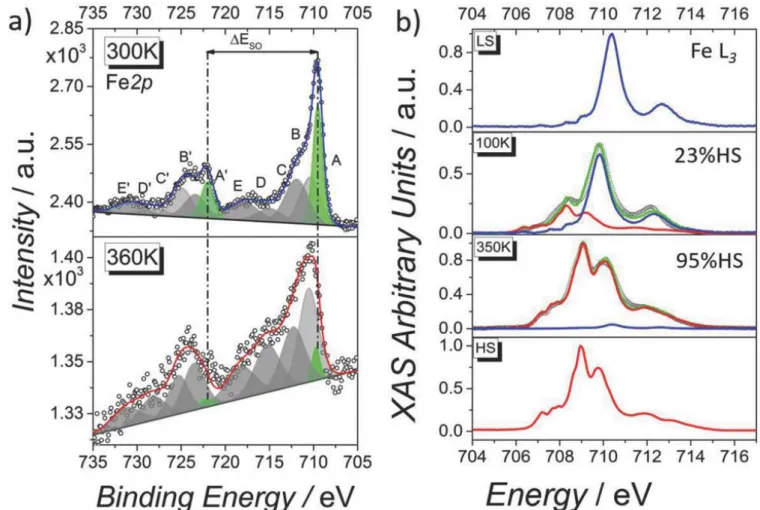
To follow the SCO transition we acquired XPS and UPS spectra at 298 and 360 K, and XAS at 100 and 350 K. In the XPS spectra (see Figure 2a) the Fe2p region is clearly different at 300 and 360 K thus providing evidence for thermally induced SCO in 6.7 nm thin film. The occurrence of SCO is particularly clear when considering the Fe2p3/2 peak that is centered at 710.5 eV in the HS state and at 709.5 eV in the LS
configuration. In the LS state this peak also appears narrower, and is principally dominated by a component at lower binding energy (709.5 eV, highlighted in green and called A) which is known to be due to the coupling of the photoelectrons with the partially‐filled metal shell.42 The spin–orbit splitting (ΔESO) value also changes significantly upon conversion, with values of 13 and 12.5 eV for the HS and the
LS components, respectively, which is in good agreement with previously reported values.43-46 Indeed, ΔESO changes upon SCO due to different orbital populations in the two spin states: in the HS
configuration the measured transition involves eg‐like orbitals that are unoccupied in the LS state. We
used a peak fitting procedure (Figure 2a) to deconvolute the spectra. The intensity of the components unequivocally attributable to the LS state (A and Aʹ in Figure 2a) allow, qualitatively, to follow the SCO transition. XPS binding energies (B.E.), percentage of the different component, and spin–orbit splitting values (ΔESO) are reported in Table S2 in the Supporting Information.46, 47 We tested the stability of the
bulk phase of 1 under X‐Ray in ultra high vacuum (UHV) conditions by cycling back to 100 K (see Figure S2b in the Supporting Information). In line with what was previously observed by Shalabaeva et al.,19
the presence of water inside the crystalline plane seems to be relevant for the occurrence of the SCO. Therefore, a reversible SCO could not be observed in the sublimated films under UHV conditions due to the loss of water. It is noteworthy that on the contrary, the SQUID measurement on a 100 nm thick film, does show a reversible SCO (Figure 1b). Nevertheless, XPS probes only the first few tens of nanometer of the sample, while magnetic measurements probe the whole of the sample, so the former is certainly more sensitive to vacuum‐induced loss of water.
Figure 2 : a) Temperature dependence of the Fe2p XPS spectra evidencing thermal SCO behavior for 6.7 nm thick films of 1 on
TS
(empty black dots) along with high‐spin Fe (II) and low‐spin Fe (II) spectra obtained from the bulk (red and blue lines, respectively) and used as reference signals for the spectral linear interpolation (green lines).
Further evidence for the occurrence of thermally driven SCO in the thin films of 1 on TSAu was obtained from UPS by analyzing the film at 300 and 360 K. This characterization, performed on the pristine film at 300 and 360 K (corresponding to the LS and the HS states, respectively) was compared with a DFT‐based modeling that helped to clarify the observed effects. The UPS spectrum acquired on a 6.7 nm film at 300 K (Figure S3, blue line, Supporting Information) evidences a highest occupied molecular orbital (HOMO) contribution at ‐2.82 eV, in agreement with similar systems7, 45, 48, 49 and the total density of states (TDOS) obtained from the DFT calculation results starting from the LS crystal structure. The temperature effect on the UPS spectra is visible mainly in the valence‐Fermi region (from 0 to 6 eV). Indeed, upon warming up from 300 to 360 K, we observed a shift to −2.35 eV (Figure S3, red line, Supporting Information) in line with what was previously reported for similar SCO compounds,7, 45, 46, 48, 49 and again in very good agreement with the TDOS obtained from the DFT calculations results starting from the HS crystal structure. Our in‐house spectroscopic analysis points out that evaporated ultrathin films of 1 on TSAu, retain the switchability of the bulk complex 1 even after thermal sublimation.
A quantitative analysis of the population of the HS and LS states was also made by XAS measurements, since absorption techniques are unmatched tools to qualitatively and quantitatively analyses ultrathin layers of molecular systems, providing the required sensitivity to monitor the spin state of the investigated system.38, 50-53 Figure 2b displays the Fe(II) L3 edge absorption spectrum of a 6.7 nm thin
film of 1 on TSAu at 100 and 350 K. The 100 K spectrum clearly shows the coexistence of LS and HS forms, which is in line with what we observed by magnetometry for a 100 nm film evaporated on Kapton (Figure 1b). A series of consecutive spectra recorded at 100 K on the very same position show the same FeL3 line shape within the noise error (Figure S4, Supporting Information) confirming the stability under
X‐Ray irradiation. Upon heating from 100 to 350 K the spectral features related to HS‐Fe(II) increase from a contribution of about 23% to ≈95%, respectively (see the Experimental Section for details). Atomic force microscopy (AFM) imaging measured on thin films of 1 (see Figure S5 in the Supporting Information) showed a rather smooth surface to confirm a nice defect‐free SCO deposit excluding the presence of defective areas or Volmer–Weber growth. The AFM estimated roughness in an area of 4 µm2 resulted at about 0.4 nm (Figure S5, Supporting Information).
2.3 Electrical Measurements
In the light of the quality of the films we obtained, we incorporated the ultrathin SCO deposits on TSAu in vertical tunnel junctions using an EGaIn top electrode as depicted in Figure 1a. The choice of the substrate is dictated by the necessity to use an ultraflat bottom electrode to obtain functional, nonshorted junctions, over hundreds of square micrometers. We contacted those thin films with EGaIn conical tips top electrodes as described elsewhere,29 and made contacts of ≈100 µm in diameter. We controlled the temperature of the system with a Linkam microscope stage, and the resulting J/V curves exhibited the typical nonlinear behavior expected for nonshort‐circuited tunnel junctions. We started with a 9.5 nm thick film, but currents measured at room temperature were too close to our instrument's lowest range (Figure S6, Supporting Information), so we switched to a 6.7 nm film in order to have unambiguous results.
The 6.7 nm thick junctions in the LS state (20 junctions, 200 traces, on a single film) present log |J| values of −7.82 ± 0.45 and −7.55 ± 0.37 at −1.0 and +1.0 V, respectively (Figure S7c, Supporting Information). The standard deviations of those measurements are in line with those observed previously for EGaIn junctions incorporating SAMs of small organic molecules.25, 28, 54 The high reproducibility of those measurements and the absence of short‐circuits are a further confirmation of the high quality of
the ultrathin SCO films we used in the junction, and of the reliability of EGaIn as the method of choice for measuring such systems.
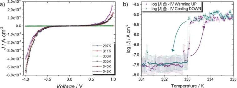
With the 6.7 nm thick film, the J/V curves registered at 297 and 340 K (corresponding to the temperature of LS and the HS states determined by magnetometry, XPS and XAS, respectively) are very strikingly different, and they provide evidence for switchable junctions with a clearly different behavior depending on the spin state of 1 (Figure 3a). Above T1/2, with compound 1 in the HS state, the tunneling
current density at 1 V applied bias potential is about two orders of magnitude higher than for the LS state (with tunneling current densities of ≈5 × 10⁻⁶ A cm−2 to ≈3 × 10⁻⁸, respectively). We also noted that the HS junction presents a moderate negative rectifying behavior, with the current flowing under negative bias being slightly larger than the one flowing at positive bias, which can be rationalized by considering that the HOMO of the compounds are brought within the conducting potential window at sufficiently negative biases (see Figure S9 in the Supporting Information).
Figure 3 : a) The complete series of J/V curve from 297 to 345K acquired with a rate of 15 mV s−1; b) log |J| at V = −1 V reported as a function of temperature acquired in sweeping mode using a rate of 1 K min−1 (warming up and cooling down,
violet and cyan respectively); the curved arrows are a guide for the eyes to emphasize the jump in electrical conductivity. To investigate the temperature‐driven switching behavior of the junction more in depth, and to verify that the great difference in current density we observed between low and high‐temperature data truly arises from the change of the spin state, we characterized the junctions at different temperatures. Figure S7b (Supporting Information) shows the obtained values of log |J| measured at an applied bias of ±1 V. To establish just how abrupt the switching phenomenon is, we repeated the measurements while increasing and decreasing continuously the temperature at a rate of 1 K min−1 (see Figure 3b) and found no significant temperature difference between the switching temperature in warming and cooling modes. Measurements in sweeping and stepping mode showed the same abrupt change in current density of approximately two orders of magnitude in the temperature window in which we expected the SCO to happen, at a critical temperature T* of 333 K (we report the complete series of log |J|/V curves in Figure S7a together with Fowler–Nordheim plots in Figure S8 in the Supporting Information). The transition voltage spectroscopy (TVS) analysis provides transition voltage values of the order of 0.1–0.6 V, but those values are likely related to some density of states in the oxide layer covering the EGaIn tip, as shown by Ricœur et al.55
Extending the variable temperature measurement to junctions made on the 9.5 nm film evidenced the same transition, though with a smaller change in current density upon the transition (see Figure S6 in the Supporting Information). As said above the lower current densities are very likely biased by our experimental setup and residual currents, and thus overestimated. Overall, it is noteworthy that our junctions all presented an abrupt SCO‐induced conductance switching, contrary to what was reported
by Shalabaeva et al. when measuring a 10 nm thick film of this SCO complex in an ITO/SCO/Al junction.21 This difference in behavior together with major differences in current densities between the two sets of experiments could have a variety of explanations. For instance, the differences in current densities could be ascribed to the differences in work functions due to the use of different electrode materials, to the fact that evaporated electrodes are known to display much higher current densities than EGaIn or mercury electrodes due to the improved effective contact with the underlying layer,29 or possibly to phenomena related to the interfaces with the electrodes (stress, electronic coupling). On the other hand, the discrepancy in conductance switching behavior could be also possibly linked to the soft nature of our top electrode that unlike rigid, evaporated top electrodes permits the required geometrical deformations of the molecular thin films at the transition temperature. It is difficult to ascertain which are the most relevant parameters, and rigorous testing of all of those hypotheses would require a separate, dedicated study. Preliminary data on another compound showing a SCO transition below room temperature, where the EGaIn ceases to be liquid and becomes much more rigid, could be ascribed to support the rigidity hypothesis and will be reported in due course.
2.4 Theoretical Model
To rationalize the experimental data and in particular to explain the magnitude of the change in current density caused by the SCO we modeled the behavior of the junctions with a single‐orbital Simmons‐like formalism that combines molecular orbital energies obtained from gas‐phase density functional theory (DFT) calculations and experimentally determined temperature‐dependent high‐spin fractions. We thus sought to reproduce the trends in tunneling current density as a function of temperature. For tunnel junctions consisting in a monolayer of molecules sandwiched between two electrodes, it has been shown that the model developed by Simmons'56-58 provides a reasonably simple way to describe the current flowing through the system.59, 60 Nevertheless, this model applies to homogeneous monolayer thin films consisting of a single compound, and it is not directly applicable to mixed multilayer stacks made up of compounds with different electronic configurations. We therefore adapted the classical Simmons' model to describe such a system by taking into account a random distribution of HS and LS molecules to compute the temperature dependent tunneling current density by adjusting the statistical population of the two states to the one determined experimentally (see the details of the model in the Supporting Information). We used DFT at the B3LYP/6‐31++G(d,p) level to estimate the gas‐phase orbital energies of the HS and LS compounds. For both HS and LS states, the calculated orbital energies for the highest occupied molecular orbitals (−5.8 and −6.2 eV, respectively) are closer to the Fermi energy function of the electrodes (−5.1 eV for Au and −4.2 eV for EGaIn) than the energies of the unoccupied molecular orbitals (−2.2 and −1.1 eV, respectively). Based on these results, assuming that tunneling is responsible for charge transport in our thin films, one would expect hole tunneling to be the dominant charge transport mechanism, and we therefore chose to take into account only the effect of hole tunneling in our model.
For both HS and LS states, we computed an approximated TDOS by homogeneous broadening of the orbital energies combined with an arbitrary rigid shift of 3.5 eV which provided DOS spectra that matched reasonably well the experimental UPS data (see Figure S3 in the Supporting Information). Combining the uncorrected orbital energies obtained by DFT with our mixed multi‐layer Simmons‐like model, we could simulate the tunneling current density as a function of temperature, by taking the temperature‐dependent HS fraction we determined experimentally. The curves generated by using magnetometry data on bulk samples and thin film samples (see Figure S10 in the Supporting Information) do not provide a good agreement in terms of absolute current density values but the empirical corrections we used were established for SAMs of organic molecules, and minor adjustments of those parameters (in particular the relative carrier mass m*) could change the absolute values of current densities in a major way. Nevertheless, our model does provide an acceptable estimation of the
expected change in the log |J| values when transitioning between the HS and LS states, with a small discrepancy between T1/2 and T* (8 and 1 K, respectively). They fail to reproduce the exceedingly abrupt
transition observed experimentally (surprisingly for such a nanoscale SCO system), exhibiting instead a more gradual conversion. While our tunneling data differ significantly from earlier reports, the relatively good agreement between our experimental and theoretical values is a strong argument in favor of using soft, conformal contacts (like EGaIn) for the characterization of transport properties of soft, pressure‐dependent molecular ultrathin films. We have no direct evidence on the exact nature of the transport mechanism in both films we measured. Nevertheless, given the lack of temperature dependence that would support a thermally activated multistep hopping mechanism, in spite of the rough assumptions underlying the Simmons model, its ability to predict the correct change of conductivity upon spin crossover is remarkable. Most importantly, it underlines that we have built a molecular junction where materials, thicknesses and electrodes materials allows for resistance switching to be governed by the change of the MO levels and not by the bulk conductance of the SCO material.
3 Conclusions
In conclusion, we have shown through a detailed spectroscopic analysis that it is possible to prepare high‐quality continuous ultrathin films of the [Fe(HB(tz)3)2] spin‐crossover complex on gold, and that such thin films can exhibit a SCO behavior similar to that of the bulk material. Building upon this fundamental preliminary finding, we studied vertical EGaIn tunnel junctions of 1, a nondamaging technique generally used for simpler molecular systems, to probe the electronic state of a 6.7 nm film. The resulting device presented a two orders of magnitude change in current density upon spin state switching. Strikingly, this change occurred in a very abrupt manner in less than 1 K, which is not at all what is usually expected for SCO complexes when shaped at that scale, where elastic cooperative effects are not enough to provide abrupt transitions or hysteretic effects.13 Altogether, the strategy we proposed and used to follow the spin state switching of the compounds in a passive SCO junction demonstrates the possibility to design large area switchable SCO tunnel junctions of ultrathin films (where SCO is induced thermally). This represents an important milestone toward the use of such junctions in the near future for the development of novel active spintronic devices in which the SCO layer could be used as a molecular switch, triggered by more complex stimuli including light irradiation and voltage pulses. Most importantly, our study also emphasizes the crucial importance of the interplay between the molecular material and its electrodes, which requires in depth fundamental analysis.
4 Experimental Section
Synthesis: Reagents were purchased commercially and used without further purification. MeOH was
distilled over Mg(OMe)2 under nitrogen. KHB(trz)3 (Htrz = 1H‐1,2,4‐triazole) was prepared according to
the reported experimental procedure61 and recrystallized in MeOH. [Fe(HB(trz)3)2] was obtained by
layering 15 mL of a degassed aqueous solution of KHB(trz)3 (1.02 g, 4 mmol) over 5 mL of a solution of
FeSO4.7H2O (0.56 mg, 2 mmol) in degassed water. The square‐shaped purple crystals that formed were
washed with water and Et2O, and then crushed in a mortar. The resulting powder was dried under
vacuum heating around 50 °C, and then purified by sublimation at 280 °C onto a cold finger under 2.10−6 mbar vacuum using a turbomolecular pump protected with a liquid nitrogen trap. Yield: 208 mg (42%). Calculated for C12H14B2FeN18 (487.83 g mol−1) C 29.54, H 2.89, N 51.68%; found C 29.41, H 2.94, N
51.23%. X‐ray diffraction of the powder obtained after purification by sublimation showed perfect matching with the reported LS structure of the anhydrous complex reported previously, with no alteration whatsoever over weeks (Figure S11, Supporting Information).18
Magnetic Measurements: Bulk magnetic measurements were performed on a Microsense EZ7 Vibrating
was weighed accurately in a silver capsule, cold‐sealed, and glued to a ∅3 mm carbon fiber rod with double‐faced scotch tape. DC measurements were performed under a 10 kOe magnetic field. Nitrogen gas was used for temperature control. Background subtraction was performed using a closely matched silver capsule. The diamagnetic contribution from the sample was estimated using Pascal's constants. For the thin film on Kapton, the compound was evaporated as a 100 nm thick 6 × 90 mm strip on to a 10 × 10 cm 50 µm thick Kapton foil. The calculated volume of 54 × 1018 Å3 corresponds to 0.174 µmol of the compound when considering the unit cell of the reported structure at room temperature. The foil was then wrapped tightly in a small cylinder perpendicularly to the strip, then placed into a straw to be introduced in a Quantum Design MPMS‐7XL SQUID magnetometer. The DC measurement was performed using a RSO head under 20 kOe magnetic field. Raw data were treated as described in reference 62.
Sample Deposition: The evaporations were performed in a Plassys thermal evaporator connected to a
glove box system. An alumina crucible was filled with the powder of 1 and once the pressure reached the 10−7 mbar range, the temperature was gently raised up to the evaporation temperature. The evaporation rate was followed by a quartz microbalance, and was stabilized in the 0.05 nm s−1 range at a temperature of 450–480 K. The tooling factor was determined by evaporating a thick film of 1 on an ultraflat silicon wafer through a soft porous membrane, and by checking the thickness of that film ex situ by AFM (see Figure S5 in the Supporting Information for details). For a target thickness of 20 nm, an actual film thickness of 27 ± 4.7 nm was measured, which corresponds to a tooling factor of 135%. This value was then used to correct the thickness of the thin films prepared for physical characterizations, and therefore obtained films with corrected thicknesses of 6.7 nm (for a target thickness of 5.0 nm) and 9.5 nm (for a target thickness of 7.0 nm).
XPS and UPS Characterizations: XPS experiments were carried out in a UHV apparatus with a base
pressure in the 10−10 mbar range. Monochromatized Al Kα radiation was used for XPS measurements (1486.6 eV, 100 W). The detector was a SPECS PHOIBOS 100 hemispherical analyzer mounting a 2D‐DLD detector, the angle between the analyzer axis and the X‐ray source was 54.44°. The XPS spectra were measured with a fixed pass energy of 40 eV. The binding energy (BE) scale was calibrated setting the Au4f signal of the substrate at 83.9 eV. In order to minimize air exposure and atmospheric contamination, samples were mounted on the sample holder inside a glovebox directly connected with the fast‐entry lock system of the XPS chamber. UPS spectra were measured using the He II line (40.8 eV) from a non‐monochromatized gas discharge lamp and the same analyzer used for XPS, yielding an energy resolution of 0.18 eV. The spectra were taken in normal emission, and they were energy calibrated using the Fermi level. The variable temperature experiment was performed by using an e‐beam heater system connected to the XPS/UPS sample holder. Every spectrum represented herein results from averaging four spectra collected after 1 h of thermalization at a specific temperature. Spectral analysis consisted in a linear background subtraction and deconvolution using a mixed Gaussian and Lorentzian line‐shape for each spectral component. The stoichiometry was calculated by peak integration, using theoretically estimated cross‐section for each transition.63
Synchrotron Characterization: The XAS experiments were performed on thin film samples at the DEIMOS
beamline64 of the SOLEIL Synchrotron facility. The flux of photon was reduced to prevent any radiation damage. None was observed. A magnetic field up to 20 kOe was applied along the photon propagation direction with the normal to the surface. The reported XAS spectra were acquired at the L2,3 edges of Fe
(applied parallel to the X‐ray propagation vector) and using the two circular polarizations (left, σ+ and right, σ‐) at normal incidence (θ = 0°). All the spectra were normalized following the procedures described in earlier reports.65, 66 Absorption spectra were measured in total electron yield (TEY) detection mode to guarantee the optimal detection sensitivity. The estimation of the temperature dependence of the HS‐Fe(II) molar fraction of the evaporated coverage was performed through
least‐squares interpolation of its normalized L3 XAS spectra with the ones of the bulk compound,
featuring temperature dependence as recorded in similar experimental conditions.67
Electrical Measurements: In order to measure the current through the molecular thin films, a liquid
top‐electrode of eutectic gallium indium alloy (EGaIn) was used. EGaIn oxidizes readily in ambient conditions to form a thin passivating oxide layer (mostly composed of Ga2O3) that allows to fabricate
tips with a controlled geometry.27 The so‐called “selected conical tips” were used as top‐electrodes on SCO films. To form stable contacts, the tips were brought close to the substrates until the tip apex wrinkling or deforming on the substrate could be clearly observed (by optical microscopy). The data on Figure 3 were acquired after a systematic thermalization time of 5 min and are the average of 12 J/V traces acquired in two different junctions (i.e., different position on the surface). For each individual tip, one junction (i.e., contact) was formed and J–V traces were recorded for forward bias 0→−V→V and J–V traces for the reverse bias V→−V. This procedure was used to avoid using a tip contaminated with absorbed impurities. The temperature control was achieved using a Linkam cryostat, and the I/V curves were acquired under nitrogen flux to avoid any oxidation of the molecular film upon increasing temperature. Each temperature corresponds to a different junction on the surface of the nanostructured surface, and for each temperature were acquired 1 sequence as described above. The temperature scale was calibrated by using a Pt‐100 thermocouple to measure the effective temperature of the AuTS substrate. Due to the low magnitude of the currents measured in the junctions (often of the order of 1 to a few pA), the built‐in potential contributed to a non‐negligible offset of the I/V curves and the data were thus systematically corrected by subtracting the 0 bias current for every junction.
Theoretical Calculations: The orbital energies were estimated by performing single‐point DFT
calculations using the crystal‐structures as input geometries without performing any optimization step, with the B3LYP functional and the 6–31++G(d,p) basis set as implemented in the Gaussian 09 program.68 The TDOS spectra were computed by Gaussian broadening of the molecular orbital energies (after a rigid shift of 3.5 eV) using the Multiwfn software.69
Acknowledgements
This work was supported by the French National Research Agency (ANR) Investment for the Future Programme IdEx Bordeaux (ANR‐10‐IDEX‐03‐02) and the Mexican government via the National Council of Sciences and Technology (CONACyT, program 073096, announcement 291060). Computer time for this study was provided by the computing facilities MCIA (Mésocentre de Calcul Intensif Aquitain) of the Université de Bordeaux and of the Université de Pau et des Pays de l'Adour. The authors acknowledge the ELORPrintTec platform, the LCPO laboratory, all the ICMCB and DEIMOS (SOLEIL) staff for their support during the measurements.
Conflict of Interest
The authors declare no conflict of interest.
References
1 - O. Kahn, C. Jay Martinez, Science 1998, 279, 44.
2 - C. Bartual‐Murgui, A. Akou, C. Thibault, G. Molnár, C. Vieu, L. Salmon, A. Bousseksou, J. Mater. Chem. C 2015, 3, 1277.
3 - J. Linares, E. Codjovi, Y. Garcia, Sensors 2012, 12, 4479. 4 - E. Ruiz, Phys. Chem. Chem. Phys. 2014, 16, 14.
5 - C. Lefter, S. Rat, J. S. Costa, M. D. Manrique‐Juárez, C. M. Quintero, L. Salmon, I. Séguy, T. Leichle, L. Nicu, P. Demont, A. Rotaru, G. Molnár, A. Bousseksou, Adv. Mater. 2016, 28, 7508.
6 - G. Molnár, S. Rat, L. Salmon, W. Nicolazzi, A. Bousseksou, Adv. Mater. 2018, 30, 17003862. 7 - K. Senthil Kumar, M. Ruben, Coord. Chem. Rev. 2017, 346, 176.
8 - N. Baadji, S. Sanvito, Phys. Rev. Lett. 2012, 108, 1.
9 - C. Lefter, V. Davesne, L. Salmon, G. Molnár, P. Demont, A. Rotaru, A. Bousseksou, Magnetochemistry 2016, 2, 18.
10 - P. Gütlich, H. A. Goodwin, Spin Crossover in Transition Metal Compounds I, Springer, Berlin, Heidelberg 2004. 11 - M. A. Halcrow, Spin‐Crossover Materials: Properties and Applications, John Wiley & Sons Ltd, Oxford, UK 2013.
12 - A. Bousseksou, G. Molnár, L. Salmon, W. Nicolazzi, Chem. Soc. Rev. 2011, 40, 3313.
13 - G. Félix, W. Nicolazzi, M. Mikolasek, G. Molnár, A. Bousseksou, Phys. Chem. Chem. Phys. 2014, 16, 7358. 14 - P. Gütlich, A. Hauser, H. Spiering, Angew. Chem., Int. Ed. 1994, 33, 2024.
15 - C. Janiak, T. G. Scharmann, H. Hemling, D. Lentz, J. Pickardt, Chem. Ber. 1995, 128, 235. 16 - C. Janiak, J. Chem. Soc. Chem. Commun. 1994, 0, 545.
17 - C. Janiak, T. G. Scharmann, J. C. Green, R. P. G. Parkin, M. J. Kolm, E. Riedel, W. Mickler, J. Elguero, R. M. Charamunt, D. Sanz, Chem. ‐ Eur. J. 1996, 2, 992.
18 - S. Rat, K. Ridier, L. Vendier, G. Molnár, L. Salmon, A. Bousseksou, CrystEngComm 2017, 19, 3271.
19 - V. Shalabaeva, S. Rat, M. D. Manrique‐Juarez, A.‐C. Bas, L. Vendier, L. Salmon, G. Molnár, A. Bousseksou, J.
Mater. Chem. C 2017, 5, 4419.
20 - M. D. Manrique‐Juarez, F. Mathieu, V. Shalabaeva, J. Cacheux, S. Rat, L. Nicu, T. Leïchlé, L. Salmon, G. Molnár, A. Bousseksou, Angew. Chem., Int. Ed. 2017, 56, 8074.
21 - V. Shalabaeva, K. Ridier, S. Rat, M. D. Manrique‐Juarez, L. Salmon, I. Séguy, A. Rotaru, G. Molnár, A. Bousseksou, Appl. Phys. Lett. 2018, 112, 013301.
22 - N. Paradis, F. Le Gac, P. Guionneau, A. Largeteau, D. Yufit, P. Rosa, J.‐F. Létard, G. Chastanet,
Magnetochemistry 2016, 2, 15.
23 - A. Diaconu, S. L. Lupu, I. Rusu, I. M. Risca, L. Salmon, G. Molnár, A. Bousseksou, P. Demont, A. Rotaru, J. Phys.
Chem. Lett. 2017, 8, 3147.
24 - P. Guionneau, E. Tailleur, M. Marchivie, J. Itié, P. Rosa, N. Daro, Chem. Eur. J. 2018,. 25 - C. a. Nijhuis, W. F. Reus, J. R. Barber, G. M. Whitesides, J. Phys. Chem. C 2012, 116, 14139.
26 - L. Cademartiri, M. M. Thuo, C. A. Nijhuis, W. F. Reus, S. Tricard, J. R. Barber, R. N. S. Sodhi, P. Brodersen, C. Kim, R. C. Chiechi, G. M. Whitesides, J. Phys. Chem. C 2012, 116, 10848.
27 - R. C. Chiechi, E. A. Weiss, M. D. Dickey, G. M. Whitesides, Angew. Chem., Int. Ed. 2008, 47, 142.
28 - M. Baghbanzadeh, F. C. Simeone, C. M. Bowers, K.‐C. Liao, M. Thuo, M. Baghbanzadeh, M. S. Miller, T. B. Carmichael, G. M. Whitesides, J. Am. Chem. Soc. 2014, 136, 16919.
29 - F. C. Simeone, H. J. Yoon, M. M. Thuo, J. R. Barber, B. Smith, G. M. Whitesides, J. Am. Chem. Soc. 2013, 135, 18131.
30 - C. A. Nijhuis, W. F. Reus, J. R. Barber, M. D. Dickey, G. M. Whitesides, Nano Lett. 2010, 10, 3611. 31 - N. Nerngchamnong, L. Yuan, D.‐C. Qi, J. Li, D. Thompson, C. A. Nijhuis, Nat. Nanotechnol. 2013, 8, 113.
32 - L. Yuan, N. Nerngchamnong, L. Cao, H. Hamoudi, E. del Barco, M. Roemer, R. K. Sriramula, D. Thompson, C. A. Nijhuis, Nat. Commun. 2015, 6, 6324.
33 - P. J. van Koningsbruggen, J. S. Miller, Solid State Sci. 2008, 10, 1804.
34 - V. Shalabaeva, M. Mikolasek, M. D. Manrique‐Juarez, A.‐C. Bas, S. Rat, L. Salmon, W. Nicolazzi, G. Molnár, A. Bousseksou, J. Phys. Chem. C 2017, 121, 25617.
35 - M. Nishino, K. Boukheddaden, Y. Konishi, S. Miyashita, Phys. Rev. Lett. 2007, 98, 1. 36 - J. A. Real, A. B. Gaspar, M. C. Muñoz, Dalton Trans. 2005, 0, 2062.
37 - H. Spiering, K. Boukheddaden, J. Linares, F. Varret, Phys. Rev. B 2004, 70, 184106. 38 - S. Brooker, Chem. Soc. Rev. 2015, 44, 2880.
39 - N. Paradis, G. Chastanet, T. Palamarciuc, P. Rosa, F. Varret, K. Boukheddaden, J. F. Létard, J. Phys. Chem. C 2015, 119, 20039.
40 - D. R. Kumar, S. Kesavan, M. L. Baynosa, J.‐J. Shim, Electrochim. Acta 2017, 246, 1131.
41 - J. Chastain, R. C. King, J. Moulder, Handbook of X‐Ray Photoelectron Spectroscopy: A Reference Book of Standard Spectra for Identification and Interpretation of XPS Data, Physical Electronics, Eden Prairie, MN, USA 1995.
42 - Y. G. Borod'ko, S. I. Vetchinkin, S. L. Zimont, I. N. Ivleva, Y. M. Shul'ga, Chem. Phys. Lett. 1976, 42, 264. 43 - E. C. Ellingsworth, B. Turner, G. Szulczewski, RSC Adv. 2013, 3, 3745.
44 - K. Burger, C. Furlani, G. Mattogno, J. Electron Spectrosc. Relat. Phenom. 1980, 21, 249.
45 - A. Pronschinske, R. C. Bruce, G. Lewis, Y. Chen, A. Calzolari, M. Buongiorno‐Nardelli, D. A. Shultz, W. You, D. B. Dougherty, Chem. Commun. 2013, 49, 10446.
46 - L. Poggini, M. Milek, G. Londi, A. Naim, G. Poneti, L. Squillantini, A. Magnani, F. Totti, P. Rosa, M. M. Khusniyarov, M. Mannini, Mater. Horizons 2018, 5, 506.
47 - L. Y. Johansson, R. Larsson, J. Blomquist, C. Cederström, S. Grapengiesser, U. Helgeson, L. C. Moberg, M. Sundbom, Chem. Phys. Lett. 1974, 24, 508.
48 - X. Zhang, T. Palamarciuc, P. Rosa, J. F. Létard, B. Doudin, Z. Zhang, J. Wang, P. A. Dowben, J. Phys. Chem. C 2012, 116, 23291.
49 - E. Ludwig, H. Naggert, M. Kalläne, S. Rohlf, E. Kröger, A. Bannwarth, A. Quer, K. Rossnagel, L. Kipp, F. Tuczek,
Angew. Chem., Int. Ed. 2014, 53, 3019.
50 - H. Wende, M. Bernien, J. Luo, C. Sorg, N. Ponpandian, J. Kurde, J. Miguel, M. Piantek, X. Xu, P. Eckhold, W. Kuch, K. Baberschke, P. M. Panchmatia, B. Sanyal, P. M. Oppeneer, O. Eriksson, Nat. Mater. 2007, 6, 516. 51 - M. Bernien, H. Naggert, L. M. Arruda, L. Kipgen, F. Nickel, J. Miguel, C. F. Hermanns, A. Krüger, D. Krüger, E. Schierle, E. Weschke, F. Tuczek, W. Kuch, ACS Nano 2015, 9, 8960.
52 - H. Naggert, J. Rudnik, L. Kipgen, M. Bernien, F. Nickel, L. M. Arruda, W. Kuch, C. Näther, F. Tuczek, J. Mater.
Chem. C 2015, 3, 7870.
53 - G. Poneti, L. Poggini, M. Mannini, B. Cortigiani, L. Sorace, E. Otero, P. Sainctavit, A. Magnani, R. Sessoli, A. Dei,
Chem. Sci. 2015, 6, 2268.
54 - C. M. Bowers, K. Liao, H. J. Yoon, D. Rappoport, M. Baghbanzadeh, F. C. Simeone, G. M. Whitesides, Nano
Lett. 2014, 14, 3521.
55 - G. Ricœur, S. Lenfant, D. Guérin, D. Vuillaume, J. Phys. Chem. C 2012, 116, 20722. 56 - J. G. Simmons, J. Appl. Phys. 1963, 34, 238.
57 - J. G. Simmons, J. Appl. Phys. 1963, 34, 2581. 58 - J. G. Simmons, J. Appl. Phys. 1963, 34, 1793. 59 - A. Vilan, J. Phys. Chem. C 2007, 111, 4431.
60 - H. B. Akkerman, R. C. G. Naber, B. Jongbloed, P. A. van Hal, P. W. M. Blom, D. M. de Leeuw, B. de Boer, Proc.
Natl. Acad. Sci. USA 2007, 104, 11161.
61 - S. Trofimenko, J. Am. Chem. Soc. 1967, 89, 3170.
62 - T. Palamarciuc, J. C. Oberg, F. El Hallak, C. F. Hirjibehedin, M. Serri, S. Heutz, J.‐F. Létard, P. Rosa, J. Mater.
Chem. 2012, 22, 9690.
63 - J. J. Yeh, I. Lindau, At. Data Nucl. Data Tables 1985, 32, 1.
64 - P. Ohresser, E. Otero, F. Choueikani, K. Chen, S. Stanescu, F. Deschamps, T. Moreno, F. Polack, B. Lagarde, J.‐P. Daguerre, F. Marteau, F. Scheurer, L. Joly, J.‐P. Kappler, B. Muller, O. Bunau, P. Sainctavit, Rev. Sci. Instrum. 2014, 85, 013106.
65 - M. Perfetti, M. Serri, L. Poggini, M. Mannini, D. Rovai, P. Sainctavit, S. Heutz, R. Sessoli, Adv. Mater. 2016, 28, 6946.
66 - L. Margheriti, D. Chiappe, M. Mannini, P.‐E. Car, P. Sainctavit, M.‐A. Arrio, F. B. de Mongeot, J. C. Cezar, F. M. Piras, A. Magnani, E. Otero, A. Caneschi, R. Sessoli, Adv. Mater. 2010, 22, 5488.
67 - B. Warner, J. C. Oberg, T. G. Gill, F. El Hallak, C. F. Hirjibehedin, M. Serri, S. Heutz, M.‐A. Arrio, P. Sainctavit, M. Mannini, G. Poneti, R. Sessoli, P. Rosa, J. Phys. Chem. Lett. 2013, 4, 1546.
68 - M. J. Frisch, G. W. Trucks, H. B. Schlegel, G. E. Scuseria, M. A. Robb, J. R. Cheeseman, G. Scalmani, V. Barone, B. Mennucci, G. A. Petersson, H. Nakatsuji, M. Caricato, X. Li, H. P. Hratchian, A. F. Izmaylov, J. Bloino, G. Zheng, J. L. Sonnenberg, M. Hada, M. Ehara, K. Toyota, R. Fukuda, J. Hasegawa, M. Ishida, T. Nakajima, Y. Honda, O. Kitao, H. Nakai, T. Vreven, J. A. Montgomery, J. E. Peralta, F. Ogliaro, M. Bearpark, J. J. Heyd, E. Brothers, K. N. Kudin, V. N. Staroverov, R. Kobayashi, J. Normand, K. Raghavachari, A. Rendell, J. C. Burant, S. S. Iyengar, J. Tomasi, M. Cossi, N. Rega, J. M. Millam, M. Klene, J. E. Knox, J. B. Cross, V. Bakken, C. Adamo, J. Jaramillo, R. Gomperts, R. E. Stratmann, O. Yazyev, A. J. Austin, R. Cammi, C. Pomelli, J. W. Ochterski, R. L. Martin, K. Morokuma, V. G.
Zakrzewski, G. A. Voth, P. Salvador, J. J. Dannenberg, S. Dapprich, A. D. Daniels, Farkas, J. B. Foresman, J. V Ortiz, J. Cioslowski, D. J. Fox, Gaussian 09, Revis. A02, Gaussian, Inc., Wallingford CT 2009.