HAL Id: tel-00670162
https://tel.archives-ouvertes.fr/tel-00670162
Submitted on 14 Feb 2012
HAL is a multi-disciplinary open access archive for the deposit and dissemination of sci-entific research documents, whether they are pub-lished or not. The documents may come from teaching and research institutions in France or abroad, or from public or private research centers.
L’archive ouverte pluridisciplinaire HAL, est destinée au dépôt et à la diffusion de documents scientifiques de niveau recherche, publiés ou non, émanant des établissements d’enseignement et de recherche français ou étrangers, des laboratoires publics ou privés.
Applications
Luis Lolis
To cite this version:
Luis Lolis. Agile Bandpass Sampling RF Receivers for low power Applications. Micro and nan-otechnologies/Microelectronics. Université Sciences et Technologies - Bordeaux I, 2011. English. �tel-00670162�
Université Bordeaux 1
Les Sciences et les Technologies au service de l’Homme et de l’environnement
THÈSE
PRÉSENTÉE A
L’UNIVERSITE BORDEAUX I
ÉCOLE DOCTORALE DES SCIENCES PHYSIQUES ET DE L’INGÉNIEUR
Luis, LOLIS
POUR OBTENIR LE GRADE DE DOCTEUR
SPÉCIALITÉ : Microélectronique
Agile Bandpass Sampling RF Receivers for low
power Applications
Soutenue le : 11 mars 2011 Après avis de :
M. REBAI, Chiheb MCF-HDR Sup’Com Tunisie Rapporteur M. LOUMEAU, Patrick PR TELECOM Paris-Tech Rapporteur
Devant la commission d’examen formée de :
M. ENZ, Christian PR CSEM Président
M. DALLET, Dominique PR ENSEIRB Directeur de Thèse M. BEGUERET, Jean-Baptiste PR Université Bordeaux I Co-directeur de Thèse M. PELISSIER, Michael Ph.D.-Eng. CEA-Leti Encadrant de Thèse M. JOET, Loïc Eng. ASYGN Examinateur M. REBAI, Chiheb MCF-HDR Sup’Com Tunisie Examinateur M. LOUMEAU, Patrick PR TELECOM Paris-Tech Examinateur
A Luma, A ma famille et à ceux qui me sont chers.
A
A
c
c
k
k
n
n
o
o
w
w
l
l
e
e
d
d
g
g
m
m
e
e
n
n
t
t
s
s
Before starting this manuscript, I would like to thank the people who made possible this work. First, my sincere thanks to my advisor Dr. Michael Pelissier, for his guidance, expertise and encouragement. I also would like to show my gratitude to Dr. Carolynn Bernier and Mr. Eric Mercier for their time and precious help organizing and correcting the publications and this manuscript. I am very grateful to my thesis supervisor Prof. Dominique Dallet from ENSEIRB and thesis co-supervisor Prof. Jean-Baptiste Bégueret from Université Bordeaux I, for their valuable academic advices and supervision.
I also thank the jury members: Dr. Chiheb Rebai, professor at Ecole Supérieure des Communications de Tunis, Dr. Patrick Loumeau, professor at TELECOM Paris-Tech, Dr. Nicolas Delorme and Mr. Daniel SAIAS, CEO/CTO at Asygn Company and Dr. Christian Enz, researcher from CSEM, for accepting to participate to the Jury.
I would like to thank Mr. Pierre Vincent, LAIR laboratory Head at CEA-LETI and Mr. Jean-René Lèquepeys, DACLE department Head at CEA-LETI, for giving me the opportunity of doing this interesting and also challenging research topic. This work wouldn’t be possible without the many helps and advices from all people in the LAIR laboratory, and for that I am extremely grateful. I also thank every DACLE member, particularly to Mrs Armelle De Kerleau for her kindness and Dr. Marc Belleville for his wise advices for the publication of the thesis results.
ACKNOWLEDGMENTS ... III CONTENTS ... IV
CHAPTER 1 :INTRODUCTION...1
1 THE EMERGING NEEDS FOR AGILE AND LOW POWER RFTRANSCEIVERS...2
1.1 The WPAN, WBAN and WS&AN - A Multitude of Low Power Applications on the ISM Band...2
1.2 Technological Trends towards Discrete Time Signal Processing: On the Interest of Bandpass Sampling ...3
2 PRESENTATION OF THE THESIS WORK...4
CHAPTER 2 :THE BANDPASS SAMPLING PROCESS & THE STATE OF THE ART ...7
1 INTRODUCTION...8
2 THE BANDPASS SAMPLING...8
2.1 Theoretical analysis...8
2.2 The voltage and charge sampling ...13
3 AN OVERVIEW OF RFDOWN-CONVERSION AND FILTERING ON DISCRETE-TIME ARCHITECTURES...17
3.1 Architectures Classification...17
3.2 Nyquist-like sampling RX ...18
3.3 RF/IF Bandpass Sampling with Single Path Filters RX...20
3.4 RF/IF Bandpass Sampling with complex filtering RX...22
3.5 A Comparative Table Summarizing the DT architectures ...24
4 DISCRETE TIME RECEIVER BASE BLOCKS STATE OF THE ART...25
4.1 LNA...25
4.2 Frequency Transposition...26
4.3 Frequency Synthesis Blocks ...28
4.4 Filtering Blocks ...30
4.5 Analog to Digital Converter...37
5 CONCLUSION...38
CHAPTER 3 :SYSTEM LEVEL MODELING AND DESIGN METHODOLOGY...41
1 INTRODUCTION...42
2 DETAILED FRAMEWORK ON THE IEEE802.15.4 AND BLUETOOTH LOW ENERGY PHY-LAYER...43
2.1 General Aspects...43
2.2 Sensitivity ...45
2.3 Linearity ...46
2.4 Channel Selection and the Interference / Blocking Performance ...47
2.5 Dynamic Range...49
3 SYSTEM LEVEL DESIGN METHODOLOGY...50
3.1 Definition of ADC Saturation - Maximum Gain and Adjacent Signal Filtering...51
3.2 Definition of required SNR and SNR degradation (Noise Figure and Noise Aliasing) 52 3.3 Definition of SNDR degradation - IIP3 test bench and specification ...53
3.4 Definition of the Filtering Specifications - Anti-aliasing, Image and Aliasing Interferer Rejection...55
C
3.5 ADC equivalent NF and IIP3 into resolution and SFDR...56
4 SYSTEM LEVEL SIMULATION TOOL...58
4.1 Basic Simulation Flow...58
4.2 Mathematical Principles on the System Level Simulation Tool...60
4.3 Base Blocks Modeling...62
5 CONCLUSION...66
CHAPTER 4 :QUANTITATIVE COMPARISON AND DEFINITION OF A BANDPASS SAMPLING RF RECEIVER ARCHITECTURE ...71
1 INTRODUCTION...72
2 FS AND F0:THE NYQUIST-LIKE SAMPLING...73
2.1 Architectural Description ...73
2.2 Filtering Techniques & Frequency Plan...74
2.3 System Level Design and Validation ...77
3 FS AND F0:RFBPS WITH QUADRATURE SAMPLING...80
3.1 Architectural Description ...80
3.2 Filtering Techniques & Frequency Plan...81
3.3 System Level Design and Validation ...82
4 FS AND F0:IFBPS WITH SINGLE PATH FILTERING...85
4.1 Architectural Description ...85
4.2 Filtering Techniques & Frequency Plan...86
4.3 System Level Design ...87
5 NEW ARCHITECTURE PROPOSITION: HIGH IFBANDPASS SAMPLING COMBINED WITH A COMPLEX DT FILTERING TO LOW-IF...91
5.1 Architectural Description ...91
5.2 Frequency Plan...92
5.3 The filtering techniques and the filtering masks ...97
5.4 System Level Design and Validation ...101
5.5 Conclusions on the Proposed Architecture...108
6 CONCLUSION...109
CHAPTER 5 : IMPLEMENTATION OF THE COMPLEX IIR FILTER ...115
1 INTRODUCTION...116
2 GENERAL PRINCIPLES OF THE IIR COMPLEX FILTER...117
2.1 Basic concept of a Discrete Time filter ...117
2.2 The Finite Impulse Response (FIR) filter...117
2.3 The Infinite Impulse Response (IIR) filter ...119
2.4 Complex discrete time filtering - Hilbert Transform ...122
2.5 Implementation of the proposed complex IIR filter ...125
3 ANALYTICAL APPROACH ON THE IMPERFECTIONS...131
3.1 Introduction to block imperfections...131
3.2 IIR Group delay impact on the EVM ...131
3.3 Impact of the filter coefficients finite resolution and the unit capacitance definition 133 3.4 Impact of the technological dispersion on the TF ...135
3.5 Noise analysis ...139
4 VHDL-AMS BEHAVIORAL MODELING FOR IIR COMPLEX FILTER...142
4.1 Motivation, modeling and validation test benches ...142
4.2 The parasitic capacitances impact on the filter TF...148
4.3 Timing Management - The Clock Tree and RC Time Constants ...150
4.4 OTA impact on the filter TF ...151
5 CONCLUSION...154
CHAPTER 6 :THE PHASE NOISE SPECIFICATIONS ON THE PROPOSED ARCHITECTURE 163 1 INTRODUCTION...164
2 CONTEXT -THE PHASE NOISE IMPACT IN CLASSICAL ARCHITECTURES...165
2.1 The Phase Noise Consideration in the Mixing Operation ...165
2.2 The Phase Noise Consideration in the Nyquist Sampling Operation ...166
2.3 The Bandpass Sampling System and Motivations for the Study ...168
3 THE JITTER IMPACT ANALYSIS...169
3.1 Analytical Approach - The Bandpass Sampling with Uncorrelated Jitter ...169
3.2 Numerical Approach to Analyze Arbitrary Phase Noise Impact on Bandpass Sampling ...172
4 CASE STUDIES...175
4.1 Method Applied on a GFSK Modulated Signal in Presence of Aperture Jitter Combined with Synthesis Jitter...175
4.2 Jitter Analysis in Presence of Interferer ...180
5 APPLICATION OF THE PHASE NOISE ANALYSIS TO THE SYSTEM LEVEL SCALING...185
5.1 Review on the Reference Architecture and the Block to Evaluate Phase Noise ...185
5.2 Defining Specifications on Phase Noise for BT-LE and IEEE802.15.4 on the Proposed Architecture...186
5.3 Impact on the Power Consumption of the Phase Noise Specifications for Bandpass Sampling ...193
6 CONCLUSIONS...194
CHAPTER 7 :CONCLUSION AND PERSPECTIVES...203
1 GENERAL CONCLUSIONS AND RESULTS...204
2 LIST OF CONTRIBUTIONS...207
2.1 Conference Publications...207
2.2 Patent...207
2.3 Projects Deliverables...207
2.4 Journal Paper...207
2.5 Presentations, Seminars and non-reviewed reports...207
3 PERSPECTIVES...208
BIBLIOGRAPHY ...209
GLOSSARY...216
RESUME ETENDU...219
1 INTRODUCTION...219
2 LA METHODE DE CONCEPTION SYSTEME ET L’OUTIL DE SIMULATION SYSTEME...220
3 COMPARAISON QUANTITATIVE ET DEFINITION D’UNE NOUVELLE ARCHITECTURE DE RECEPTION A SOUS ECHANTILLONNAGE...221
4 IMPLEMENTATION DU FILTRE COMPLEXE A TEMPS DISCRET A RII...222
5 SPECIFICATIONS EN BRUIT DE PHASE POUR L’ARCHITECTURE PROPOSEE...223
:
C
C
h
h
a
a
p
p
t
t
e
e
r
r
1
1
:
Introduction
Introduction
CHAPTER 1 : INTRODUCTION... 1 1 THE EMERGING NEEDS FOR AGILE AND LOW POWER RFTRANSCIEVERS... 2
1.1 The WPAN, WBAN and WS&AN - A Multitude of Low Power Applications on the ISM Band... 2 1.2 Technological Trends towards Discrete Time Signal Processing: On the Interest of Bandpass Sampling ... 3 2 PRESENTATION OF THE THESIS WORK... 4
1 The Emerging Needs for Agile and Low Power
RF Transceivers
1.1 The WPAN, WBAN and WS&AN - A Multitude of Low
Power Applications on the ISM Band
The Wireless Personal Area Network (WPAN) is limited to some tens of meters range
(<100m) and low- to medium- data rate (< 3 Mbps). Furthermore, the WPAN has evolved and led to the consideration of other networks such the Wireless Body Area Network (WBAN) and
Wireless Sensor & Actuator Network (WS&AN). WPAN applications have been standardized by the
15th working group of IEEE802 and is split in 7 task groups. The low data rate WPAN defines
the 4th task group leading to the IEEE802.15.4 specifications, whereas Bluetooth had been
considered by the first task group, therefore IEEE802.15.1. Primarily, it was created to link small devices and peripherals with a computer, not specifically for data transfer, although in some applications this data is processed and further sent to a wider network. Following the publication of 802.15.1-2005, the IEEE Study Group 1b voted to discontinue their relationship with the Bluetooth SIG. Later versions of Bluetooth are not IEEE standards. Therefore the Bluetooth Low Energy that we apply in our study is not part of the IEEE802.15 working group.
The Bluetooth standard was created in 1994 by Ericsson. It was defined for a data rate around 1 Mbps and 30m communication distance range. Lately, the Bluetooth 2.0 EDR extended the data rate up to 3 Mbps. The Bluetooth standard is particularly adapted to file transfer applications and connections between a PC and peripheral appliances, known as Piconet, where up to 8 devices can be connected in this network. The first device is the master and all the other devices are slaves communicating with the master. As mentioned before, Bluetooth got apart from IEEE in 2005 and developed its own solutions in the WPAN area. Lately, it was perceived that the Bluetooth devices and specifications were not optimized in terms of power consumption, mostly for lower distances applications (up to 10m).
The concept of Wireless Body Area Network (WBAN) was created mainly for medical and sport applications, such as heart beat monitoring and other body condition status. In this application the data rate is not the main issue but the service quality is very demanding. The most recent version, Bluetooth 4.0 integrates a low power section specification called Bluetooth Low
Energy (BT-LE) which objective is mainly to increase battery life for communication devices in
the WBAN context. This work is focused on the low power configuration of Bluetooth. On the IEEE802.15 side, the concept of WBAN was also explored. Created in 2007, the task group IEEE802.15.6 is developing a communication standard optimized for low power devices, operating around the human body (but not limited to humans) covering a variety of applications, such as medical, Consumer Electronics, personal entertainment to name a few. In this case, there is a direct competition in terms of applications and band in use (the advantage of IEEE802.15.6 compared to BT-LE is to cover various bands other than the 2.4 GHz Industrial, Scientific and
As previously mentioned, the IEEE802.15.4 was created by the 4th IEEE802.15 task
group. It was particularly interested in low data rate and high latency times. These characteristics are also well adapted to low cost, ultra low power and low data rate applications. It started to be widely used in industrial processes, now moving from Wireless Sensor Network (WSN)to Wireless
Sensor & Actuator Network (WS&AN), where the network configuration is automatically set with
the addition / suppression of nodes on the network. The IEEE802.15.4 is historically also applied for medical applications on the WBAN context [1]. The standard occupies three different bands: 868MHz (Europe), 915 MHz (USA) and 2.4 GHz worldwide.
The motivation on multistandard applications comes from the variety of Physical Layer
Device (PHY) and Media Access Control (MAC) layers specifications in the 2.4 GHz ISM band, and
even wider variety of specifications from the network layer protocols (Layer 3) to upper layers which can run over IEEE802.15.4-based networks, including ZigBee. Observing this promising field of applications, and considering that the 2.4 GHz ISM band is in most cases addressed by these standards, we propose to develop innovative receiver architecture capable of addressing this variety of standards in the WPAN, WBAN and WS&AN context. The most remarkable standard technologies for short range, IEEE802.15.4 and Bluetooth Low Energy, are the starting references for this work.
1.2 Technological Trends towards Discrete Time Signal
Processing: On the Interest of Bandpass Sampling
RF transceivers that require a lot of analog components do not fully benefit from technological scaling. As a consequence, analog blocks and base band blocks such as Digital Base
Band Processor (DBB) and the Application Processor (APP) do not progress similarly, the latter being
best-adapted to deep-submicron technologies scaling. In such technologies, the strongest drawback limiting analog functions performances are the low voltage supply and high threshold voltages. In other words, there is considerable reduction on the voltage headroom to implement analog functions. On the other hand, the improvements on the switching characteristics of MOS transistors offer excellent time accuracy, and lithography offers precise control on the capacitance ratios [2]. Considering these trends, Mitola first envisaged the concept of Software Defined Radio (SDR) [3]. All the RF and base band stages are digital, through the application of an Analog to
Digital Converter (ADC) directly connect to the antenna. It is evident that the ADC required
performances should fulfill extraordinary specifications, and in this case becomes incompatible with the mandatory energy-efficient context. Although digital communication standards occupy frequency bands from 800 MHz to 6 GHz, the bandwidth of a single channel, goes to a maximum of 20MHz, apart from Ultra Wide Band (UWB) standards. Therefore, demodulation and base band processing can be reduced to this frequency in order to have multistandard digital circuitry. Signal processing operations prior to the ADC can be actually reduced to amplification, filtering and downconversion.
The idea to merge SDR concepts with power consumption constraint considerations and consists in using Discrete-Time receivers. One major argument is the possibility to exploit the natural technological scaling trend, while avoiding the weaknesses, such as reduction of voltage headroom or increasing technology variability ([2]-[4]). Theses trends are summarized and
detailed in [5]. Analog discrete-time circuits, such switched-capacitor networks, are adapted to implement the amplification, down-conversion and filtering operations mentioned above.
A particular interesting process that can be exploited on the context of Discrete Time receivers is the Bandpass Sampling (BPS). The BPS is one kind of Discrete Time receiver which permits conversion from Continuous Time (CT) domain to Discrete Time (DT) domain while also operating the down-conversion. The application of this principle is also motivated by the fact that the useful information occupies a bandwidth which is considerably lower than the carrier frequency. The front-end samples only the useful information, making possible to reduce both frequency synthesis and circuit cutoff frequencies. In order to apply the BPS and DT signal processing concepts into low power applications, it is even more interesting to further reduce the sampling frequency by applying high under-sampling ratio combined to anti-aliasing filters prior to the sampler Once the signal is in DT domain, process such as DT filtering, based on the principle of capacitance charge sharing, and decimation, can be applied to reduce the sampling frequency and to reject unwanted signals / interferers. Finally, these techniques enable the reduction of the ADC constraints in terms of clock frequency and resolution.
The new challenges when designing BPS receivers come from the aliasing of the spectrum while under-sampling and processing decimation. An optimized frequency plan has to be designed as well as some filtering techniques to overcome interferer’s aliasing into the band of interest. Another considered aspect is to simplify the filtering networks by merging CT and DT filter techniques. We present in this work new methodologies and simulation tools able to address these various system level challenges in order to propose a new BPS architecture oriented to low power consumption and multi-standard purposes. The idea of designing a DT reconfigurable and low power receiver merges the technology trends towards the deep-submicron technologies and the evolution on the WPAN 2.4GHz ISM applications and standards.
2 Presentation of the Thesis Work
The objective of this thesis work is to propose and specify new receiver architectures able to address characteristics of both agile multi-standard and ultra low power receivers, exploring the BPS technique. In CHAPTER 2, the BPS theory is presented. We highlight the new challenges in terms of the system level design that the BPS process unveils. An overview of the various RF DT receiver architectures is presented. The idea is to set some original ways for down-conversion and filtering based on DT signal processing by merging different solutions and bringing the best of each, exploiting current available literature. On the following, the critical blocks state of the art in the receiving path is presented. The performances of the state of the art set the reference for low power system level design. CHAPTER 3 presents a system level simulation tool developed in MATLAB. Wide-band modeling is implemented to take into consideration the specificity of BPS receivers. A system level specification method which rapidly converges to the standard requirements is also presented. Using the proposed method and associated tool, a quantitative comparison has been carried out for different BPS architectures and is presented in CHAPTER 4. The system level design and block specifications over the
various architectures permit to have more insight on the DT architectures trade-offs. A particular attention is brought on the filtering optimization of the receiver chain between the continuous time elements (BAW, Lamb filters) and discrete time elements (switched capacitor active or passive networks). The carried out study ends by a proposition of a new RF BPS receiver architectures based on a high intermediate frequency and a complex DT filtering, regarded as the best trade-off between power consumption and agility. The derived block specifications are compared to the state of the art of the CHAPTER 2 in order to strengthen the work towards a low power goal.
The complex DT filtering function presenting Infinite Impulse Response (IIR) is a key component of the proposed architecture. This filter has a reduced order for a high selectivity and rejection performance while avoiding drawbacks coming from zero IF architectures, such 1/f noise, DC-offset, I/Q mismatches and second order non linearity. CHAPTER 5 presents the theory of DT filtering and its implementation on silicon. The objective of CHAPTER 5 is to validate the DT filter and to evaluate the impact of circuit implementation imperfections on the required frequency response. To achieve this goal, two approaches were adopted, analytical development on the imperfections and behavioral modeling simulation. The analytical approach is defined in terms signal and noise, in order to dimension capacitance sizes. From there, the behavioral modeling is applied further evaluate the circuit imperfections such as parasitic capacitances and non-linear parameters.
:
The
Bandpass
Sampling
Process
&
the
State
of
the
Art
C
C
h
h
a
a
p
p
t
t
e
e
r
r
2
2
: The Bandpass
Sampling Process & the State of
the Art
1 INTRODUCTION...8
2 THE BANDPASS SAMPLING...8
2.1 Theoretical analysis...8
2.2 The voltage and charge sampling ...13
3 AN OVERVIEW OF RFDOWN-CONVERSION AND FILTERING ON DISCRETE-TIME ARCHITECTURES...17
3.1 Architectures Classification...17
3.2 Nyquist-like sampling RX ...18
3.3 RF/IF Bandpass Sampling with Single Path Filters RX...20
3.4 RF/IF Bandpass Sampling with complex filtering RX...22
3.5 A Comparative Table Summarizing the DT architectures ...24
4 DISCRETE TIME RECEIVER BASE BLOCKS STATE OF THE ART...25
4.1 LNA...25
4.2 Frequency Transposition...26
4.3 Frequency Synthesis Blocks ...28
4.4 Filtering Blocks ...30
4.5 Analog to Digital Converter...37
1 Introduction
The DT receiver is being presented in the literature as an interesting method to merge the technological down scaling trend to further improve integration and the need for agile multi-standard transceivers. The objective of this thesis work is at the same time to optimize the concept of DT receiver on the multi-standard aspect and to improve the power consumption for low power RF communications such as WPAN, WBAN and WS&AN. The technique of BPS is being presented here as a solution to alleviate the frequency synthesis constraints thanks to the implementation of the down-conversion process and a CT to DT conversion.
Considering the DT-based architectures, BPS operation and DT signal processing like filtering and decimation are merged into the whole chain through down-conversion and filtering. This chapter focuses on the theory of BPS. New challenges in terms of system level design come with the application of BPS. Two different techniques are possible during the sampling process: the voltage sampling and the charge sampling. This chapter highlights the difference between both techniques.
Concerning the architecture itself, the frequency plan can be defined in different ways with regards to BPS and DT filtering techniques, depending on preferred options e.g.; oriented towards multi-standard or low power applications for instance. In this chapter, the State of the Art (SOA) of the DT receivers is presented. We define a classification method based on the down-conversion process, the frequency plan and filtering techniques. Three orthogonal families of DT receivers can be mentioned in the SOA. They are compared in terms of agility and power consumption characteristics. The distinct BPS configurations defined in this chapter are further applied in the ISM band and the Ultra Low Power (ULP) standards, in order to lead a quantitative comparison in Chapter 4.
In this chapter, since the system level design of this work is low power oriented, we study the SOA on blocks whose power consumption is critical in RF transceivers. This includes the
Low Noise Amplifier (LNA), Mixer, Sample-and-Hold (S/H) blocks, but also the frequency synthesis
ones such as Phase-Locked Loop (PLL) and Delay-Locked Loop (DLL). The scope of this SOA concerns the 2.4GHz ISM band. Furthermore, on the system level design, the derived specifications provided in Chapter 4 will be compared to the retrieved SOA performances in order to demonstrate the feasibility of the proposed DT architectures in a low power context.
2 The Bandpass Sampling
2.1 Theoretical analysis
The conversion from the analog to the digital domain is composed by two distinct operations: first from continuous time to discrete time domain and then from continuous amplitude to discrete amplitude domain. Sampling a signal means observing a given value from a continuous time waveform at a given time instant. During the uniform sampling process the values of the
waveform are observed at the instants nTS, where TS is called the sampling period. The sampling
process is modeled by two distinguished operations: the multiplication of the input signal vin(t)
(Figure 2-1) by an infinite sequence of Dirac pulses, and a discretization in time and frequency domain [6, 7]:
n S in n S in S int
v
t
t
nT
v
nT
v
_
(2-1)
n S in S n S S in S inV
f
nf
T
nf
f
T
f
V
f
V
_1
1
(2-2)The convolution by a sequence of Dirac pulses in the frequency domain means that the sampled signal is periodic in frequency at fs=1/TS (2-2) (Figure 2-5). The signal vin_s(t) (Figure
2-1) is still defined in CT-domain. The second operation is the discretization of vin_s(t) to vin[n].
While applying the DT Fourier Transform, we observe the discrete spectrum with a normalized frequency range r=f/fs. Lately, we show that the DT signal processing is not exclusive of the digital domain (discrete amplitude), but also possible on the analog domain (continuous amplitude). The sampled spectrum in the normalized frequency “r” domain is obtaining by substituting f=r .f S:
n S S in S S infs
r
n
T
f
r
V
f
r
V
_1
(2-3)From the scaling property of the Dirac delta function [8] which defines:
fs
n
r
n
r
fs
(2-4)We infer that the scaling coefficient 1/Ts disappears on the DT spectrum. Defining Vin_S(r)=Vin_S(r.fs), we have:
n in n in S inr
V
r
r
n
V
r
n
V
_
(2-5)The important difference is that the scaling factor 1/TS only exists in CT domain, and
disappears after the CT-to-DT conversion [6]. The Bandpass Sampling, also known as sub-sampling, considers a sampling frequency which does not respect the strict Nyquist-Shannon Criterion [9, 10] fs>2.f
H, where fH is the highest frequency of the signal to be sampled. The BPS
theory is a generalized interpretation of the Nyquist-Shannon Theorem [11]. A bandpass signal vin_RF(t) is a signal where the PSD Vin_RF(f) is centered at a given center frequency f0 (Figure 2-4) with a bandwidth BWCH much lower than this f0 ( Figure 2-4). The signal is bandpass sampled
vin_RF_s(t), respecting the Nyquist-Shannon criterion fs>2.BWCH. The signal PSD is again periodic
at fs (Figure 2-6) with an image of the signal falling into the lower band, the base band or an intermediate frequency.
0 0.2 0.4 0.6 0.8 1 -0.4 -0.3 -0.2 -0.1 0 0.1 0.2 0.3 0.4 t(s) A vin(t) vin-s(t) 0 0.2 0.4 0.6 0.8 1 -0.4 -0.3 -0.2 -0.1 0 0.1 0.2 0.3 0.4 t(s) A vin-RF(t) vin-RF-s(t)
Figure 2-1 : The base band signal over sampled: vin(t) and
vin_s(t) (fs=200Hz)
Figure 2-2 : The bandpass signal under-sampled: vin_RF(t)
f0=500Hz (fs=250Hz) -4000 -200 0 200 400 0.005 0.01 0.015 0.02 0.025 0.03 0.035 f Vin (f ) (Hz) (Hz) fS f L fH BWCH -6000 -400 -200 0 200 400 600 0.002 0.004 0.006 0.008 0.01 0.012 0.014 0.016 f(Hz) Vin -R F (f )
Figure 2-3 : Vin(f) Figure 2-4 : Vin_RF(f), f0=500Hz
-6000 -400 -200 0 200 400 600 0.2 0.4 0.6 0.8 1 1.2 1.4 1.6 x 10⁻³ f Vin -S (f) fS (Hz) (Hz) fS -6000 -400 -200 0 200 400 600 0.5 1 1.5 2x 10 -3 f(Hz) Vin -R F -s (f )
Figure 2-5 : Vin_s(f) f0=0, fs=200Hz Figure 2-6 : Vin_RF_s(f), f0=500Hz, fs=250Hz
Figure 2-1 illustrates the base input signal along with the sampled values according to the Shannon-Nyquist criterion. In Figure 2-2, the same signal is converted to f0=500Hz and Bandpass Sampled. The sampled signal PSD Vin_s(f) is given in Figure 2-5 : it is continuous and periodic at fs. In Figure 2-2, the signal input vin_RF(t) is modulated by a carrier at f0=500Hz (Figure 2-4). The signal is Bandpass Sampled compared to the carrier at fs=250Hz, leading to the
same sampled signal from the Nyquist sampling. The sampled spectrum is periodic at fs=250Hz (Figure 2-6). In both Figure 2-5 and Figure 2-6 the spectrum around the base band is the same (scaled by 1/Ts). From expression (2-5), the scaling faction 1/Ts is suppressed.
Figure 2-7 illustrates the bandpass sampled signal down-converted to the base band. The spectrum is periodic at fs, and an image of the signal at RF is convolved to the base band, and the input signal is band limited by fL and fH (Figure 2-7(a)). From Figure 2-7(b), the lowest distance
between n.fs/2 (n being even) and the center frequency of the signal sets the Intermediate
Frequency (IF) of the down-conversion Figure 2-7(c). In other words, the convolution between the Dirac pulse placed at n.fs/2 and the RF signal sets the base band signal.
f f 0 fs/2 -fs/2 -fs -nfs/2 -(n-1)fs/2 fs f 0 fs/2 fs (n-1)fs/2 (n)fs/2 (n-1)fs/2 (n)fs/2 RF signal Spectrum Sequence of Dirac Pulse Spectrum Sampled Signal Spectrum -fs/2 -fs -nfs/2 -(n-1)fs/2 fL fH (a) (b) (c) IF IF
Figure 2-7 : Frequency representation of the BPS process ; (a) the RF signal, (b) the Dirac pulses sequence, (c) the bandpass sampled signal
Observing the frequency plan presented in Figure 2-7, the following relations have to be respected in order to avoid spectrum aliasing. The value “n” is defined as the under-sampling ratio ([11]): s H f f n 2 (2-6)
2 1 L s f f n (2-7)
H s f f n 2 (2-8) 1 2 2 n f f n f L S H (2-9)The maximum allowed bandwidth is therefore derived from (2-9):
0 0
max min 2f n 1 fs , n fs 2f
The first advantage on the BPS is the down-conversion in the frequency domain and the time discretization of the signal on the same process. The second one is that low sampling frequencies can be applied in order to relax frequency synthesis. The discrete-time signal processing can still be applied in analog domain (discrete-time with continuous amplitude) in order to implement filtering process and decimation functions. These filters are referred in this thesis work as Discrete-Time filters and filters applied after the ADC are defined as Digital filters.
The drawback of the BPS process is the spectral folding of undesired signal into the band of interest (Figure 2-8 (a)). For instance, we have to consider the thermal noise, limited in a band BWnoise which represents the cut-off frequency of the sampling system. In a sampling system, the
periodicity of the spectrum implies that the wideband noise folds into each of the fs/2 bands [11]. Before sampling, consider the in-band continuous time noise PSD defined as NC_PSD (Figure
2-8) and the out-of-band noise PSD defined as NC_PSD/noise, where noise is capacity of filtering
the input noise prior to sampling. The sampled noise PSD is defined as PSDS_PSD (Figure 2-8 (b)).
The increase of noise PSD between before and after sampling process is defined as the aliasing factor, =Nout_PSD/Nin_PSD (Figure 2-8 (b)).
The signal-to-noise ratio of the sampled signal is degraded by at least the aliased noise from DC to BWnoise. Thereafter, to reduce the impact of , an anti-aliasing filter is applied which
rejects the out-of-band noise by noise. The resulting aliasing factor is defined as :
deg / 2 1 SNR fs BWnoise noise (2-11)
In BPS, the Nth harmonic of the Dirac pulses defines the down-conversion (Figure 2-8
(a)). The distance between the Nth harmonic and the signal of interest sets the Intermediate
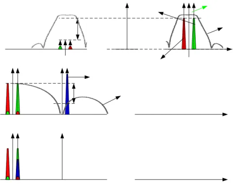
Frequency IF after sampling. In a wideband spectrum context, there can be multiple interferers folding into the band, when their frequency distance to another multiple of the sampling Dirac is also IF (Figure 2-8 (b)) : they are aliasing interferers or image interferers.
Figure 2-8 : The BPS: the spectrum before (a) and after (b) sampling
The spectrum aliasing represents the most important constraint to consider when designing BPS architectures. The accurate knowledge of the aliasing bands enables the definition of filtering techniques and frequency plan, considering the given application and specifically its frequency band in use.
2.2 The voltage and charge sampling
There are two methods to implement the sampling operation at the circuit level: the
Voltage Sampling and the Charge Sampling. Voltage sampling is a conventional method which is
implemented by Sample-and-Hold (S/H) circuit. It tracks an analog signal and stores its value as a voltage in a sampling capacitance, and keeps this voltage for some length of time. The
Charge-and-Hold (C/H) circuit integrates the signal current within a given window. The input is transferred
from voltage to charge domain before it is sampled. In the next sections, we derive the sampling transfer function in order to show the basic differences between these two techniques ([12]). The output noise divided to Gain Bandwidth (G . BW) is derived to compare the relations between
noise and power consumption for both techniques.
2.2.1 Voltage Sampling
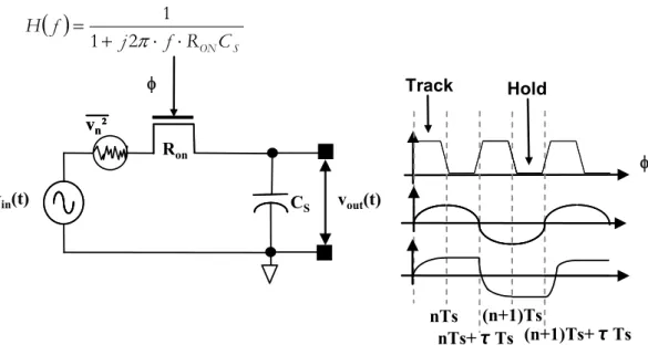
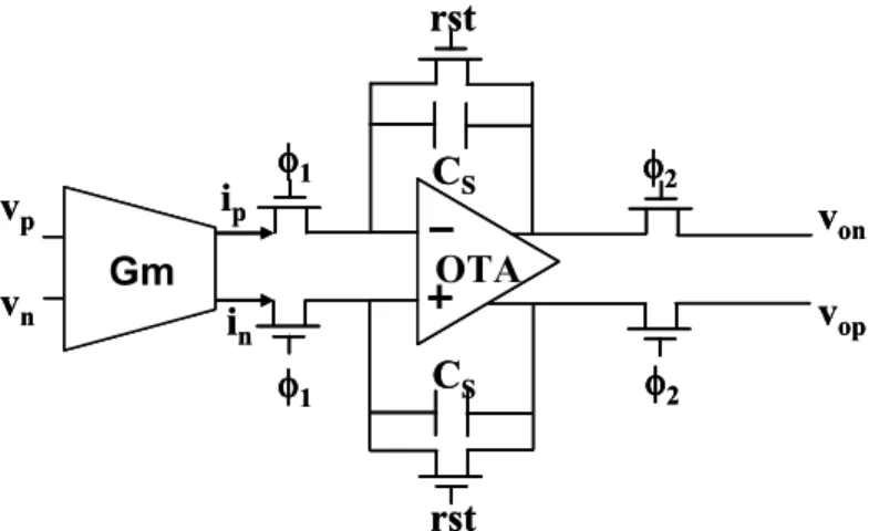
Ideally, a voltage sampling can be modeled as the input voltage signal sampled by ideal sampler (2-1). Actual implementations use the S/H block presented in Figure 2-9. The samples are considered at all nTs times. The sample is Hold between nTs and nTs+τTs, (τ is the duty cycle 0<τ<1). During the Hold period, the signal can be quantized by an ADC or DT analog signal processing can be implemented (i.e. DT filters). The next sample is tracked from nTs+τTs to (n+1)Ts. At (n+1)Ts , the next sample is considered. If, in the tracking phase, the exact value of vin(t) is hold, the sampled DT signal is the same than as defined in (2-1). On the other hand, during the tracking phase, the switch ON resistance RON and the sampling capacitance Cs
represent a low-pass filter between vout(t) and vin(t) (Figure 2-9), defined in the frequency domain as H(f):
S ONC R f j f H 2 1 1 (2-12) vout(t) vin(t) CS Track Hold nTs nTs+τTs (n+1)Ts (n+1)Ts+τTs Ron vn² vn²Figure 2-9 : The Sample-and-Hold circuit and the clock scheme
The sampled signal is therefore defined by:
r
V
r
n
V
r
n
H
r
n
V
n in n out S out
_ (2-13)In conclusion, the discrete time sequence is the application of the sampling process of a low-pass filtered Continuous Time signal.
2.2.1.1 Input Referred Noise and the Gain Bandwidth Product.
The noise generated by the S/H circuit is defined by the switch resistance RON and the
circuit cut-off frequency. The total noise is the generated PSD noise integrated along the frequency:
0 2 2 0 2 2 2 1 1 4 4 df C R f R T K df f H R T K V v S ON ON ON n
S n C KT V v 2 2 (2-14)
fs C T K Hz V PSD S H S 2 / 2 / (2-15)where k is the Boltzmann Constant, T is the temperature in Kelvin and fs=1/Ts. The input referred noise depends on the process gain on the sampling level. Consider a buffer presenting a transconductance “gm” and a unit load resistance; we observe the Gain Bandwidth (G.BW) (in hertz) product:
S C gm GBW 2 (2-16)
The output noise-to-gain bandwidth ratio is defined as follows:
fs C T K gm C BW G PSD S S 2 4 2 2 2 (2-17)
What is observed is that power consumption (in this case represented by gm) will depend on the required input referred noise figure and gain. In this section, it is shown that the choice for the sampling capacitance and for the transconductance gain infers the sampling system bandwidth, gain and noise. Small capacitances lead to high noise at constant power consumption. A third aspect is the sampling frequency which folds the KT/C noise in the fs/2 band.
2.2.2 Charge Sampling
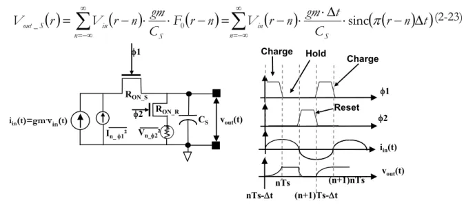
In charge sampling, the voltage is transferred into a current source, and it is integrated in CS between nTs-t and nTs (Figure 2-10). The integrated value is therefore held and reset; the
charging integration restarting at (n+1)Ts-t. The sampled voltage is defined as [13]:
gm v t u t nTs t u t nTs dt Cs dt t v gm Cs nTs v in nTs t nTs in out 1 1
(2-18)where u(t) is the unit step function. Now, let consider f0(t) defined as:
t u t t
u tf0 (2-19)
The equation (2-18) becomes:
v
t f
t
t nTs
Cs gm dt t nTs f t v gm Cs nTs vout
in in 0 0 1 (2-20)
V
f F f Cs gm f V t f t v Cs gm t vout in 0 out in 0 (2-21)Similar to H(f) defined in (2-12), F0(f) represents the frequency response for the filtering
function prior to sampling [13]:
f t
f t
F0 sinc (2-22)
Similarly to (2-5), the DT spectrum of the charge sampled signal is given by:
n S in n S in S outr
n
t
C
t
gm
n
r
V
n
r
F
C
gm
n
r
V
r
V
_ 0sinc
(2-23) iin(t)=gm.vin(t) 1 vout(t) CS Charge 1 Hold nTs-t nTs (n+1)Ts-t iin(t) vout(t) Reset (n+1)nTs 2 In_1² Vn_2² 2 RON_S RON_R ChargeFigure 2-10 : The Charge-and-Hold circuit and the clock scheme
The sinc function is an intrinsic filtering function on the charge integration, which can be considered as an anti-aliasing function. As the voltage sampling is limited by the gm and the Cs from the intrinsic low-pass function on the S/H circuit; the charge sampling is limited by Cs and gm integration process, which also represents a low-pass behavior. The cut-off frequency depends on the integration period t (and therefore on the clock), contrarily to the RC time constant for the voltage sampling. The filtering stage (H(f) F0(f)) is applied prior to sampling, therefore the filtering transfer function stages are not periodic. On the sampling process the filtered signal becomes periodic.
2.2.2.1 Input Referred Noise and the Gain Bandwidth Product.
During the charging phase, the RON resistance from the sampling switch RON_S is seen as
a current noise source, which is integrated in the defined window F0(f). The noise from the
sampling switch is defined as follows:
S S ON S S ON n C R t C T K df f F R T K V v _ 2 0 0 _ 2 2 1 _ 2 4
(2-24)The reset switch of Figure 2-10 also contributes to the noise level. During the charging phase, the noise from the reset switch is discharged (the time constant depending on the sampling switch RON_S), and at the beginning of the hold phase, it is added to the sampling switch noise:
ON S S
tRON SCS
S C R t S R ON R ON n e C T K df e C R R T K V v _ 2 2 _ 2 _ 0 _ 2 2 2 _ 2 1 1 4
(2-25)
t RON SCS S S ON S H C e C R t fs C T K Hz V PSD 2 _ _ 2 / 2 2 / (2-26)The filtering function of the charge sampling is defined by (2-21). The cut-off frequency is independent on the RON_SCS time constant, but on the integration interval t (when
sinc(ft)=0.71, i.e. ft =.0.44). The noise becomes scaled by the t/R
ONCS ratio:
S S ON S S ON S S S ON S H C C R t if C R t C KT C R t if C KT Hz V PSD _ _ _ 2 / 2 2 2 (2-27)In order to compare this with the voltage sampling, we develop the expression for the noise divided by G.BW on the charge sampling process. The gain at DC for the charge sampling
is given thanks to (2-22), G=gm.t/C
S. The -3dB cut-off frequency is defined when fct
=.0.44 (sinc(fct)=0.71), which leads to fc=0.44/t. GBW is defined as follows: 44 . 0 Cs gm BW G (2-28)
2 2 2 2 44 . 0 1 2 2 _ t RON SCS S ON S S e C R t fs C KT gm C BW G PSD (2-29)Better gain bandwidth is achieved by charge sampling for the same gm, where the noise can be as low as KT/CS for high RON_S.
2.2.3 Comparative study summary
The following table summarizes the different characteristics of both sampling techniques:
Parameters Voltage sampling Charge sampling
BW(Hz) 1/(2RONCS) 0.44/t
Noise % 1/CS % t /(RONCS)
Realization Simple V-I Converter
Resetting Structure Anti-aliasing LP filter Sinc filter
Table 2-1 : The low power and/or wideband LNA SOA
The voltage sampling is mostly dependent on the RC time constant, and for high frequencies, the switch resistance is a critical parameter to consider. At Nyquist sampling, the =2RC time constant is defined to be at least =1/(5.f
H), where fH is the highest frequency to
be sampled. The H(f) (2-12) transfer function presents a non-constant group delay g, which
leads to signal distortion. Figure 2-13 illustrates (right hand axis) the variation of the group delay in percent. At Nyquist sampling, if the time constant is one fifth of the highest sampling frequency to be sampled (=1/(5.f
H)) fH=0.2.fc, from Figure 2-11 we observe that it represents a
variation on the group delay of g=3.7%. On the other hand, in BPS process, the band occupied
by the signal is very small compared to the center frequency f0>>BWCH. For a signal centered at
the cut-off frequency of the system f0=1/, the variation of g=3.7% is observed when
f0/BWCH=12.67. In conclusion, the constraint to define RC time constant in BPS is reduced if
process. It is important to notice that the voltage sampling transfer function is independent on the sampling frequency and on the duty cycle.
On the charge sampling, the transfer function is defined by a sinus cardinal where the cut-off frequency is dependent on the sampling interval t (Figure 2-10). The charge sampling needs a linear V-I converter and a reset stage, which leads to somewhat more complex circuits. The sinus cardinal function has the advantage of presenting a transfer function with linear phase, where the cut-off frequency can be closer to fH for Nyquist sampling process. For the BPS it
becomes a drawback since the transfer function depends on the applied sampling frequency. Considering a duty cycle of t.fs=0.5, if the signal center frequency is f
0=fs, the signal is already
attenuated by a factor greater than 3dB. For higher frequencies the sinus cardinal filter will suppress the signal of interest. In order to reduce the sampling frequency, t has to be kept constant, and in this case, the duty cycle is changed. In any of cases the charge sampling becomes a constraint on the clock generation.
0 0.2 0.4 0.6 0.8 1 1.2 1.4 -5 -4 -3 -2 -1 0 |H (f)| (dB) 0 0.2 0.4 0.6 0.8 1 1.2 1.4-75 -60 -51.9 -48 -30 -15 -3.87 X: 0.9614 Y: -48.07 X: 1.039 Y: -51.93 f/fc |H(f)|(dB) g(%) g (%) 0 0.2 0.44 0.6 0.8 1 1.2 1.4 1.6 1.8 2 -40 -35 -30 -25 -20 -15 -10 -3 0 |F0 (f) |(dB) f.(t)
Figure 2-11 : The group delay relative variation in voltage
sampling Figure 2-12 : The charge sampling sinc filter
In conclusion, if lower sampling frequencies and simple clock generation are aimed at, the voltage sampling has to be preferred. For high under-sampling ratios, implemented with either voltage or charge sampling, an anti-aliasing filter is mandatory to reduce the impact of the aliasing noise. The RC time constant drawback noticed in Nyquist operations is less constraining in BPS test cases when f0>>BWCH.
3 An Overview of RF Down-conversion and
Filtering on Discrete-Time Architectures
3.1 Architectures Classification
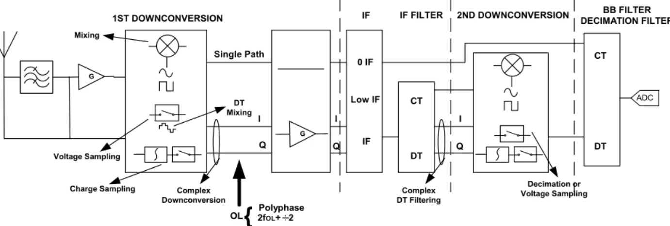
In order to classify the various DT receiver architectures, we derive a generic mapping of the possible down-conversion and filtering techniques (Figure 2-13). The studied DT architectures in the literature are [2, 4, 6, 14-20]:
G Single Path G I Q OL
{
2fPolyphaseOL+ 2 1ST DOWNCONVERSION IF 0 IF Low IF IF IF FILTER CT DT2ND DOWNCONVERSION DECIMATION FILTERBB FILTER
CT DT ADC I Q I Q Charge Sampling Voltage Sampling Mixing DT Mixing Complex
Downconversion DT FilteringComplex
Decimation or Voltage Sampling
Figure 2-13 : – Synoptic of the down-conversion and filtering techniques.
In most cases, the RF filter is mandatory, since the linearity constraints on the LNA would be impossible to fit considering low power requirements. The idea in this work is to find the fair trade-off between reconfigurability and power consumption. Software Defined Radio architectures often use wideband LNAs without any RF filters [4, 6]. When non linear LNA’s are employed, a bank of RF filters is needed to address multiple bands.
Frequency down-conversion can be implemented using classical mixer stages, where the Local Oscillator (LO) can present various waveforms. Different waveforms are implemented in order avoid harmonic intermodulation products. Charge sampling [2, 4, 15-17] and voltage sampling [6, 14, 18, 19] have also been implemented directly at RF frequencies. The first down-conversion can be implemented in single path or in quadrature. Three distinct groups appear in this classification:
- Nyquist-like sampling Receiver (RX) [2, 4, 6, 15, 16].
- RF/IF Bandpass Sampling with single path filters RX [14, 19, 20]. - RF/IF Bandpass Sampling with complex filtering RX [17, 18].
The first family of architectures presents a sampling frequency at least fs=fRF. The
minimum under-sampling ratio is n=2. We then refer this kind of process as Nyquist-like sampling RX. The second family exploits the properties of BPS in order to reduce the sampling frequency, while applying voltage sampling. Precise quadrature synthesis is needed for the complex sampling operation. The third family implements the concept of complex filtering in DT domain. The complex filter is used either to implement direct conversion with single clock generation or to implement image rejection at low-IF. On the following sections, the various receiving strategies from the SOA will be classified according to the generic scheme of Figure 2-13, and pros and cons are listed for each architecture family.
3.2 Nyquist-like sampling RX
The common point of all architectures in this family is the single down-conversion to zero- or low-IF. Quadrature frequency synthesis is therefore necessary to discriminate the receiving paths in the former case. The classification for such receivers is in Figure 2-14. Charge
and voltage sampling examples are present in this type of architecture. The related SOA for this architecture family is in [2, 4, 6, 15, 16].
The RF filter is suppressed in the case where several RF bands are desired; on the other hand more complicated DT filtering networks are implemented to achieve the required rejection and highly linear LNA are used. Although the inherent integration filter is capable to implement out-of-band anti-aliasing filtering, many out–of-band signals are still present from DC to fRF
which may saturate the amplifier stage and block the signal of interest.
Considering the inherent integration filtering of charge sampling [2, 4, 15, 16], the under-sampling ratio (2-6) is limited to 2, which leads to under-sampling frequencies as high as the RF center frequencies. The presented quadrature frequency synthesis blocks consist of a clock reference at 2.f
RF then followed by a divider-by-two. Thereby, considering the rising or the falling edges of
this division process, the quadrature clocks are generated. This technique while improving I/Q mismatches compared to polyphase Voltage Controlled Oscillator (VCO) requires generating the base frequency at least at twice the RF frequency.
G Single Path G I Q OL 2fOL+ 2 1ST DOWNCONVERSION IF 0 IF Low IF
IF FILTER 2ND DOWNCONVERSION DECIMATION FILTEBB FILTER R
DT ADC I Q [2,4,15,16] [6] [2,15] [4,6,16]
Figure 2-14 : – Down-conversion and filtering techniques for [2, 4, 6, 15, 16]
Over-sampling, and DT mixing is present in [6]. This technique allows applying Harmonic
Rejection (HR) with a DT mixing process. In [6], the generated frequency is fs=8.f
RF, where 8
different phases define a sine/cosine pair. This technique improves anti-aliasing characteristics and harmonics intermodulation rejection. The selected gains are 1:√2: -√2:-1:-1:-√2:√2:1 for cosine wave and √2:1:1:√2:-√2:-1:-1:-√2 for sine wave. The DFT of this sequence leads to a signal where the 3rd and 5th harmonics are rejected.
For all receivers considered in this section, once the signal is down-converted, successive decimations down to the ADC sampling frequency are implemented. In order to avoid the noise / interferer aliasing in the band presented in Figure 2-8, consecutive DT filtering and decimation are implemented. There is a trade -off between the DT filter / decimation circuit complexity and the ADC performances. Higher ADC sampling frequency is present in [16], where more performing DT filtering techniques are presented in [4]. In this case, the filters orders or the number of decimation steps increase. Implementing DT filtering at high fs is sensitive to parasitic capacitances and represents a constraint on the clock tree generation (mismatch and clock buffers). Figure 2-15 and Figure 2-16 illustrate the power consumption distribution for [16] and [4], respectively. Notice that the clock and the synthesis power consumptions represents from 30% to 40% of the total receiver power.
At zero-IF, careful design is required to reduce 1/f noise, DC offset and second order non-linearity [4, 6, 16]. A low-IF frequency plan is preferred in [2, 15]. Both choices suffer from I/Q mismatch: at zero-IF, it leads to EVM degradation whereas at low-IF, it leads to finite image rejection. Apart from the drawbacks of zero-IF, low-IF presents a more constraining test bench regarding I/Q mismatch, considering that the image signal is an interferer which power is higher than the signal of interest one.
21% 61% 18% DPLL Analog Clk 29% 39% 32% Clk Analog DT filter
Figure 2-15 : – Power consumption Budget for [16] Figure 2-16 : – Power consumption Budget for [4]
The sampling frequency, which sets the down-conversion, changes for each channel to be addressed. Since constant decimation order is applied, the ADC works at a variable sampling rate.
A fractional decimation is needed Between the ADC sampling frequency and the digital base band, where digital processors work at constant rate. The DT signal processing gives certain flexibility to the circuit. Consider the filtering function defined on the normalized frequency range. The filter notches are defined at multiples of the decimated frequency, meaning that they shift in absolute value with the sampling frequency. The ADC clock frequency can be reduced changing the decimation order. In conclusion, this family of architectures proposes a great agility to address various standards, considering that the reconfiguration relies on a wide frequency range synthesis and several filtering/decimation stages. A bank of RF front-end filters or highly linear LNAs are used, depending on the integration level / power consumption trade-off.
3.3 RF/IF Bandpass Sampling with Single Path Filters RX
In this case, low sampling frequencies are preferred, which implies that charge sampling is avoided. The voltage sampling S/H circuits are better adapted for that matter [14, 19, 20]. The classification for such receivers is illustrated in Figure 2-17:
G Single Path I Q 1ST DOWNCONVERSION IF 0 IF IF IF FILTER CT DT BB FILTER DECIMATION FILTER 2ND DOWNCONVERSION DT ADC I Q I Q 2fOL+ 2 OL [14] [14,15] [14] [14,15] [14] [14] [15] [15] [20] [20]
In order to reduce the sampling frequency, [20] the charge sampling becomes impractical since the inherent integration filtering rejects the signal of interest (as presented in section 2). Considering that the RF filter bandwidth correctly rejects out-of-band blockers, the sampling frequency can be reduced as low as BWRF. For direct conversion, the quadrature clock at 2.fs is
sensibly small compared with the previous architecture family. To correctly separate the I/Q signals, the under-sampling ratio is set as follows: (n/2) must be an odd number ([20]). Lately in Chapter 4, we will observe that this topology is even more sensitive to I/Q mismatch than if fs=fRF. This is the case since the phase difference multiplies over the harmonics of fs. With a low
sampling frequency and no intrinsic filtering, the voltage sampling with high “n” needs anti-aliasing filtering. For the thermal noise, smooth filtering is sufficient. For example the output noise of a tuned LNA presents low enough noise to support the aliasing factor. CT anti-aliasing at RF are implemented by Surface Acoustic Wave (SAW), Bulk Acoustic Wave (BAW), BAW Lamb
Wave Resonators (LWR) and LC tuned LNA filters.
Single path sampling can be used to avoid problems from I/Q mismatch. In [19], the first BPS sampling operation is used for down-conversion. From the first sampling process the signal is down-converted from the RF frequencies to an IF. Consider the aliasing cases illustrated in Figure 2-8, the IF must be higher than the front-end filter BW to avoid image and out-of-band aliasing. The frequency plan is defined in such a way that a single sampling frequency (fs=761.8 MHz) is applied to down-convert three RF bands (GSM, UMTS and IEEE802.11g) to the same IF (114.6 MHz to 189.2 MHz) range. Since a single fs is applied, the IF band is as wide as the RF band. To address several channels, the second sampling frequency is variable inside the IF band. The decimation ratio between the first and the second sampling frequencies is mostly non integer. The simplest way to implement this decimation is to reconvert the signal from CT-domain to DT-CT-domain, and then resampling. The CT-CT-domain to DT-CT-domain conversion is implemented by an interpolation filter at IF. The wide IF bandwidth is the main drawback of this architecture, since the filter needs a very large relative bandwidth (BWIF/IF49%). The second
sampling frequency is centered on the channel to demodulate. The complex IF sampling also suffers from I/Q mismatches, but at lower frequencies, this constraint is better overcome.
In [14], a higher under-sampling ratio of n=23 is considered, where an anti-aliasing filter is implemented at the LNA output. In this work, the same RF filter design is applied before and after the LNA. Both filters and the LNA are off-chip in this work. In [14], the sampling frequency is slightly higher than the RF BW. From the first sampling stage to the ADC, several DT filter and decimation stages are applied. The signal is down-converted to IF1=fs/3. The image signal at fRF+2fs/3 is filtered prior to sampling by RF filtering techniques. From the first
sampling frequency to the ADC clock frequency, several decimations by 2 are implemented. After the decimation process, the signal falls again at fsdec/3, where fsdec is the decimated sampling
frequency. A possible interferer that is centered at fs/6 will also fall at fsdec/3. The DT filter is
implemented in such a way to have the pass band at fs/3 and a zero at fs/6. The chosen filter type is the Bi-quadratic filter ([14]) (IIR filter). The same DT filter can be used along with all decimation stages. Low-IF and low fADC can be achieved as long as the image rejection
specification is met by the bi-quadratic filter.
This architecture family relies on reducing the sampling frequency while applying voltage BPS. Possible passive IF filtering for anti-aliasing can be implemented by BAW-Lamb filters and
SAW filters. The SOA on the filtering blocks is presented in section 4.4.2. The RF front-end filter is used as an interferers anti-aliasing filter, and tuned LNAs for noise anti-aliasing prior to sampling. Single path sampling to low-IF presented in [14] merges the sampling frequency reduction and relax 1/f noise, DC-offset and IIP2 constraints. The drawback is the DT filter implementation complexity.
3.4 RF/IF Bandpass Sampling with complex filtering RX
The complex demodulation presented in section 3.2 consists on having two sampling clocks which are shifted in phase by 90º, and, for the low-IF case study, on applying the complex sampling for image rejection. In section 3.3, single path sampling is applied with the image signal being rejected prior to sampling by a CT filter (at RF or IF). The complex sampling suffers from I/Q mismatch which will generate distortion at base band level in the case of zero-IF or limited image rejection in the case of low-IF. The image rejection implemented by CT filters is only achieved with selective filters or with relatively high IF.
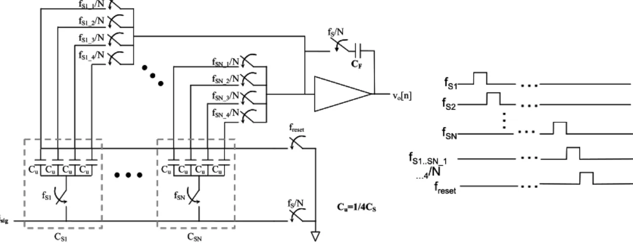
In order to avoid I/Q mismatch issues from complex sampling process and to relax or suppress off-chip CT filters, the technique of complex DT filtering is implemented in [17, 18]. The main idea is to shift the frequency response of a low-pass DT filter into an intermediate frequency using the Hilbert Transform [21]. The theory of the DT filtering, and in particular the complex DT filtering, is presented in Chapter 5. The resulting filter contains complex coefficients and is non-symmetric from a frequency point of view, enabling to filter image frequency signals. The receiving strategy of [17, 18] is summarized in Figure 2-18:
G Single Path 1ST DOWNCONVERSION IF IF IF FILTER CT DT BB FILTER DECIMATION FILTER 2ND DOWNCONVERSION DT ADC I I Q I Q [17] [17] [17] [18] [18] [18]
Figure 2-18 : – Down-conversion and filtering techniques for [17, 18]
In [18], the center frequency of the complex filter is equal to fc=fs/4. Through voltage sampling, the signal is down-converted to IF1=fc or IF1 close to fc. In [18], it has been chosen to have IF1=fc. In [18], two operating modes are observed: the first one implementing a high sampling frequency in order to reduce the S/H noise impact (2-14) and the second one applying half of the sampling frequency to observe the power savings. In Figure 2-19 and Figure 2-20 we illustrate the power budget for high and low sampling frequency modes and the power saving (20% less power consumption). The front-end filter rejects the first image frequency signal at fRF -2.IF1. The decimation implements a second down-conversion. Where IF1=fc=fs/4 (which is the
case for [18]), the signal is down-converted to zero-IF. In this case, the complex filter is used to separate I/Q signal. When fc=fs/4 the phase shift between I and Q paths transfer function at fc is /2, therefore, quadrature sampling phase shift can be implemented using a single clock reference and several filtering paths. If IF20, image rejection is implemented by using a