Digitally-Assisted, Ultra-Low Power Circuits and
Systems for Medical Applications
by
Jose
L. Bohorquez
B.S.,
University of Florida (2002)
M.S., University of Florida (2004) MASSACHUSETTS INSTatPE OF TECHNOLOGYFEB 23 2010
LIBRARIES
Submitted to the Department of Electrical Engineering and Computer Science
in partial fulfillment of the requirements for the degree of Doctor of Philosophy in Electrical Engineering
at the
MASSACHUSETTS INSTITUTE OF TECHNOLOGY
February 2010
©
Massachusetts Institute of Technology 2010. All rights reserved.A uthor ... ...
Departme of Eft cca iglineering and Computer Science January 7, 2010 Certified by .... ... Joel L. Dawson Associate Professor Thesis Supervisor Certified by .... ,... Anantha P. Chandrakasan Professor
7)
Thesis SupervisorAccepted by .. ./.
. . . .. . . . . .. .
Terry Orlando Chairman, Department Committee on Graduate ThesesDigitally-Assisted, Ultra-Low Power Circuits and Systems
for Medical Applications
by
Jose
L. Bohorquez
Submitted to the Department of Electrical Engineering and Computer Science on January 7, 2010, in partial fulfillment of the
requirements for the degree of
Doctor of Philosophy in Electrical Engineering
Abstract
In recent years, trends in the medical industry have created a growing demand for a variety of implantable medical devices. At the same time, advances in integrated circuits techniques, particularly in CMOS, have opened possibilities for advanced implantable systems that are very small and consume minimal energy. Minimizing the volume of medical implants is important as it allows for less invasive procedures and greater comfort to patients. Minimizing energy consumption is imperative as batteries must last at least a decade without replacement. Two primary functions that consume energy in medical implants are sensor interfaces that collect information from biomedical signals, and radios that allow the implant to communicate with a base-station outside of the body. The general focus of this work was the development of circuits and systems that minimize the size and energy required to carry out these two functions. The first part of this work focuses on laying down the theoretical framework for an ultra-low power radio, including advances to the literature in the area of super-regeneration. The second part includes the design of a transceiver optimized for medical implants, and its implementation in a CMOS process. The final part describes the design of a sensor interface that leverages novel analog and digital techniques to reduce the system's size and improve its functionality. This final part was developed in conjunction with Marcus Yip.
Thesis Supervisor: Joel L. Dawson Title: Associate Professor
Thesis Supervisor: Anantha P. Chandrakasan Title: Professor
Acknowledgments
Whatever challenges I have faced in life, they pale in comparison to the countless blessings God has granted me. I, therefore, thank Him above all for the great honor of having had the opportunity to study at MIT, and for giving me strength in times of difficulty.
Secondly, I thank Professors Joel Dawson and Anantha Chandrakasan for giving me the opportunity to be part of their research groups and the privilege of their guidance. Both their areas of expertise and their advising styles were complementary in a way that tremendously enriched my experience as a graduate student. They gave me the freedom to explore areas that I was interested in while guiding me to ensure my research was relevant. They were understanding when personal challenges required my absence; they were encouraging when I faced research difficulties. They also gave me access to two groups of exceptional research colleagues with a broad range of knowledge and experience that I was able to draw from to enhance my own research; a group of students who are as friendly and cooperative as they are bright. I am very grateful to the members of both research groups for sharing their ideas and always being available to bounce my own off of. I am especially grateful to Patrick Mercier and Willie Sanchez. They reviewed my papers and often offered excellent advice on my research, but more importantly, they have been great friends whom I've enjoyed spending time with. I also owe a great debt of gratitude to Marcus Yip who was a pleasure to work with and whose efforts contributed directly and significantly to my thesis.
Over the last few years, my wife and I have been blessed with a handful of great friends whom we have shared much joy with. Jaime Andres and Marlyn Echeverry have been close friends for over a decade now, and we were extremely fortunate that fate brought them to Boston for two years during which we shared times of sorrow and incredible joy. We watched Gator football together and ate many steaks. We had the blessing to be there when their daughter, little Natalia, was born, and the gift of having them with us when our daughter, Isabela, was baptized. We had
con-tentious discussions on politics and edifying conversations on faith, all along fortifying a friendship that will surely last a lifetime.
During my first year at MIT we were also fortunate to meet Hoda Eydgahi, Miriam Makhlouf, Michael Schnall-Levin, Samantha Green-Atchley, and Stephanie Gil. De-spite being a little crazy, we all helped each other keep sane by sharing in social
diversions from our academic obligations.
Although I have already thanked Willie Sanchez, I must thank him again along with his fiancee, Shirley Cardona, for being great friends over the past year. What began with their offer to baby-sit Isabela has grown into a wonderful friendship. Their love for Izzy means the world to us, and their friendship is a true blessing.
Before joining MIT and on multiple occasions during my studies, I had the good fortune to work with a team of exceptional engineers at BitWave Semiconductor. I am grateful to that entire team, especially Geoff Dawe, Russ Cyr, and Don Young
Chang. They have been good friends and invaluable mentors.
Over the last year, I have also had the great fortune of meeting Al-Thaddeus Avestruz, Michael Rinehart, Seward Rutkove, and Lynne Levitsky. The exciting endeavor of starting a company with them has been an experience of great personal growth and new aspirations. I feel humbled to be part of such a talented team and look forward to our continued collaboration with great enthusiasm.
Finally, I thank my family for their love and support. All of the opportunities I have had in life were afforded by the many sacrifices my parents, Francisco and Clara, made. My brother, Jesus Alberto, and sister, Maria Carolina, have always been examples of faith and love in my life. Throughout my studies, their support and encouragement has been constant. My nieces, Natalie, Tatiana, and Daniela, have been sources of pride and joy since their birth. I also feel blessed to have married into a wonderful family and thank Carmen, Melissa, Sebastian, Humberto, Santiago, and Valentina for the support and joy they have brought into our lives.
Of course, the person who has sacrificed most throughout the last few years and
whose unwavering support has been my greatest source of strength and comfort is my wife Natalia. She has been patient and understanding beyond reasonable
expec-tations; through wedding planning; through her pregnancy with Isabela; through our daughter's first two years; and, now, through her second pregnancy, she has always adjusted her life to lighten my load. My achievements are as much hers as they are mine, and I will always be grateful for her loving encouragement. I must also thank our daughter Isabela. Though she may not understand it now, her playful affection has brought me great peace, rest, and joy during the moments of greatest stress and frustration.
Contents
1 Introduction
1.0.1 Trends in Medical Electronics . . . . 1.0.2 Medical Implant Communication Service Band . . . . 1.0.3 Biomedical Sensor Issues . . . . 1.0.4 Research Goals and Thesis Organization . . . .
2 Frequency-Domain Analysis of Super-Regenerative Amplifiers 2.1 Introduction . . . . 2.2 General SRA Theory . . . .
2.2.1 Circuit Model and Block Diagram for SRA . . . . 2.2.2 SRAs as Time-Varying, Second-Order Systems . . . . . 2.2.3 General SRA Solution for Linear Mode Operation . . . 2.2.4 SRA Solution for a Ramp and Sine Damping Functions 2.3 Convolution Model of SRA Solution . . . . 2.3.1 SRA Response to an Arbitrary Input . . . . 2.3.2 SRA Response to a Sinusoidal Input . . . . 2.3.3 SRA Response to Multiple Sinusoids . . . . 2.3.4 SRA Response to a Pulse-Shaped Sinusoidal Input . . 2.4 Receiver Sensitivity Analysis . . . . 2.4.1 Noise Analysis using the Convolution Model . . . . 2.4.2 Solving for the BER and Sensitivity . . . . 2.4.3 Using a Time Random Variable for Detection . . . . . 2.5 Measurement Results . . . . 33 33 . . . . 35 . . . . 35 . . . . 37 . . . . 38 . . . . 40 . . . . 42 . . . . 45 . . . . 47 . . . . 50 . . . . 51 . . . . 53 . . . . 56 . . . . 57 . . . . 60 . . . . 63
2.6 Sum m ary . . . . 66
2.7 Appendix 1: Convolution yielding the variance of Ix . . . . 68
2.8 Appendix 2: Solving for the PDF of TT ... ... 69
3 Ultra-Low Power Transceiver for Medical Implant Communications 71 3.1 Introduction . . . . 72
3.2 Architecture Overview . . . . 73
3.2.1 Exploiting the Unique Features of Medical Implants . . . . 74
3.2.2 Link Analysis and Antenna Considerations . . . . 75
3.3 FSK/MSK Transmitter . . . . 77
3.3.1 FSK/MSK Theory . . . . 78
3.3.2 Transmitter Implementation . . . . 79
3.3.3 Capacitor Array with Predistortion . . . . 79
3.3.4 Setting fc and AF . . . . 82
3.4 Super-Regenerative Receiver . . . . 82
3.4.1 Super-Regeneration Theory . . . . 82
3.4.2 Receiver System Design . . . . 85
3.5 Circuit Implementation . . . . 87
3.5.1 DCO Implementation . . . . 87
3.5.2 Programmable Ramp Quench Oscillator . . . . 89
3.5.3 Envelope Detector . . . . 92
3.5.4 Programmable Comparator . . . . 93
3.6 Prototype Frequency Correction Loop . . . . 94
3.7 Measurement Results . . . . 96
3.7.1 Transm itter . . . . 97
3.7.2 Receiver . . . . 100
3.8 Sum m ary . . . . 103
4 Digitally-Assisted Sensor Interface for Biomedical Applications 105 4.1 Applications . . . . 106
4.2.1 Thermal Noise and the Noise Efficiency Factor .1
4.2.2 Flicker Noise . . . . 113
4.2.3 Using Chopping to Mitigate Flicker Noise . . . . 114
4.2.4 Power Line Interference . . . . 116
4.2.5 Techniques for Mitigating the Effects of PLI . . . . 119
4.2.6 Electrode and IAMP DC Offset . . . . 125
4.2.7 Dealing with Electrode DC Offset . . . . 126
4.2.8 Top-Level Design Requirements . . . . 127
4.3 Instrumentation Amplifier Design . . . . 128
4.4 Sinc Anti-Aliasing Filter . . . . 139
4.5 Mixed-Signal Feedback for Interference Cancelation . . . . 151
4.5.1 M otivation . . . . 151
4.5.2 PLI Considerations . . . . 154
4.5.3 Prototype System Design . . . . 155
4.6 Measurement Results . . . . 169
4.6.1 Frequency Response . . . . 173
4.6.2 Input-Referred Noise Measurement . . . . 178
4.6.3 Total Harmonic Distortion . . . . 181
4.6.4 IAMP Input Impedance . . . . 183
4.6.5 Notch Filter . . . . 186
4.7 Sum m ary . . . . 194
5 Conclusion and Future Work 195 5.1 Summary of Contributions . . . . 195
5.2 Future Work . . . . 198
A Chopper-Based IAMPs 201 A.1 A Simple Chopper-Based IAMP . . . . 201
A.2 Current Feedback IAMP with EDO Cancelation . . . . 204
A.3 OpAmp-based IAMP with EDO Cancelation . . . . 206
A.4 IAMP based on a Chopper-Stabilized OpAmp . . . . 208 110
List of Figures
1-1 Wireless link between patient and healthcare provider. . . . . 28
2-1 (a) SRA circuit model, and (b) SRA feedback loop model. . . . . 35
2-2 Time-varying pole/zero locations for an SRA as the damping function
changes. ... ... 37
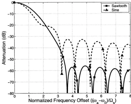
2-3 Sensitivity functions for sawtooth/ramp and sine damping functions
(7 = 3). . . . . 42
2-4 (a) Damping function, (b) sensitivity function, (c) time derivative of sinusoidal input, (d) windowed input, and (e) k(t). . . . . 44
2-5 Numerical simulations comparing the exact equation k(t) with the
convolution approximation k, (t) for y = 3 and (a) wa = wo, (b) wa = wo +2Q,, and (c) wa= wo
+
4Q.. . . . . 45 2-6 Graphical representation of SRA response to a sinusoidal input signal. 482-7 Frequency response using a sawtooth/ramp damping function and
vary-ing values of y. . . . . . . . . . . . . . . . . . . . . . . . . . . . . . . 50
2-8 Frequency response using a sawtooth/ramp and sine damping functions ( y = 3). . . . . 51
2-9 SRA (a) transconductance Gm(t), (b) damping function ((t), (c) input current ia(t), (d) output voltage for linear system v,(t), and (e) output voltage for compressive nonlinear system. . . . . 61
2-10 Schematic of SRA and envelope detector. . . . . 64
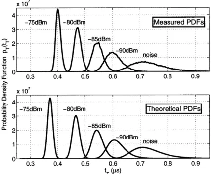
2-11 Theoretical and measured envelope detector waveforms for -75dBm and -85dBm CW input signals and two sample waveforms for no input signal (i.e. only noise). . . . . 67 2-12 Measured and theoretical probability density functions for the random
variable tT. . . . . 67
2-13 Frequency response of the SRA for Q,/(27r) = 48OkHz/vr. . . . . . 68
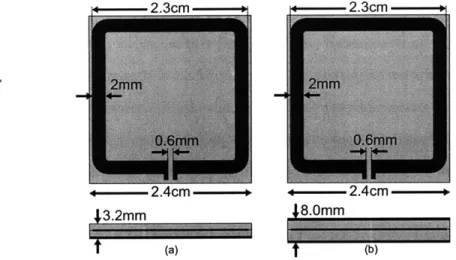
3-1 Transceiver block diagram. . . . . 73 3-2 (a) Loop antenna with FR4 substrate and superstrate, and copper
patch below the substrate. (b) Loop antenna with metal patches above and below the substrate and superstrate. . . . . 76 3-3 (a) Direct modulation FSK transmitter and (b) simplified circuit model. 78 3-4 (a) Sub-ranging capacitor array and (b) piece-wise linear predistortion. 80 3-5 Frequency steps vs. NF using linear, predistorted, and piece-wise linear
(PWL) predistorted capacitor banks. . . . . 81 3-6 (a) SRR circuit model, and (b) SRR feedback loop model. . . . . 83
3-7 (a) Differential Colpitts oscillator, (b) half circuit model, (c) equivalent half circuit, (d) noise model, and (e) equivalent noise model. . . . . . 88 3-8 Differential Colpitts digitally-controlled oscillator with predistorted
sub-ranging capacitor banks and loop antenna. . . . . 90 3-9 (a) Sawtooth oscillator, SRR bias generator, and baseband clock. (b)
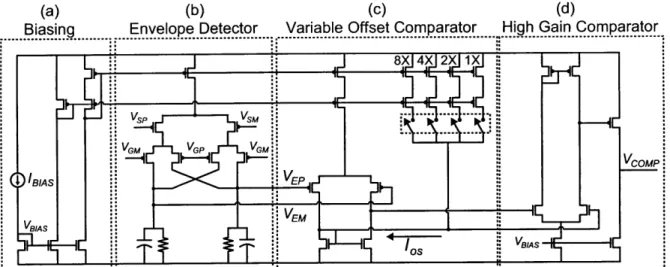
Output signals. . . . . 91 3-10 Schematic for differential envelope detector and comparator with
pro-grammable input offset voltage. . . . . 93 3-11 Measurements of the frequency correction loop including the
transi-tion of the DCO frequency, coarse tuning coefficient, and fine tuning coefficient as the channel is changed from (a) 7 to 8, (b) 1 to 10 incre-mentally, and (c) 1 to 10 in a single command. . . . . 95 3-12 Die photograph (1.0 x 0.5mm active area). . . . . 97
3-13 DCO frequency for (a) coarse, (b) medium, and (c) fine tuning. Ther-mometer coding and predistortion of each capacitor bank lead to mono-tonic, linear tuning for each range. . . . . 98 3-14 Measured spectral mask of transmitter with a data rate of (a) 200kbps
and (b) 120kbps. The signal is taken through an antenna 10cm from the transm itter. . . . . 99 3-15 Power received at an antenna placed 20cm from the transmitter and
DCO frequency vs. bias current. . . . . 100
3-16 Receiver chain time domain signals. . . . . 101
3-17 (a) Far off and (b) close in CW blocker rejection. Input signal level set to sensitivity + 6dB = -93dBm with a carrier frequency of 403.35MHz and a bit rate of 40kbps. . . . . 102
4-1 Block diagram of a typical sensor interface including the off-chip and on-chip aggressors that must be dealt with. . . . . 108 4-2 Frequency-domain analysis of the signal and noise at different stages
of a chopper-based sensor interface system. . . . . 115 4-3 Classical model for power line interference in two-electrode
measure-ments (SWE3 off), and three-electrode measurements (SWE3 on). . . 118
4-4 Simplified driven-right-leg circuit for safe common-mode voltage reduc-tion . . . . 123 4-5 Typical connection of EEG amplifiers to their respective electrodes. . 124 4-6 Electrode configuration for standard 10-20 electrode system (black
dots) with additional electrodes for 10-10 system (gray dots). Figure taken from [46] . . . . 124 4-7 Instrumentation amplifier using MOS-bipolar pseudoresistor elements
[25]. . . . . 127
4-8 Instrumentation amplifier architecture used for the work presented in this thesis. Although the chopping switches were not used, they are shown here to analyze their effect. . . . . 129
4-9 (A) Single ended equivalent of IAMP in Fig. 4-8 including noise sources, and (B) corresponding block diagram. . . . . 130
4-10 Schematic of fully differential operational amplifier including second stage choppers. These choppers are not used in normal operation but are included here for completeness. . . . 132
4-11 Simplified schematic of fully differential opamp without choppers. . . 133 4-12 (A) Frequency-domain illustration of desired signal band (white) and
aliasing components (gray) that would corrupt the signal after sam-pling. (B) A typical anti-aliasing filter amplitude response that filters aliasing components by some required amount. (C) The minimum re-quired amplitude response of an anti-aliasing filter. The dark gray boxes represent bands that can be aliased without corrupting the sig-nal band. (D) Discrete-time spectral component between -f,/2 and f,/2 illustrating how the desired channel is not corrupted and the non-filtered components of (C) are frequency translated to the bands be-tween the channel edges and the Nyquist frequencies. . . . . 141
4-13 Simplified schematic of the instrumentation amplifier and SAFF. The output voltage of the SAFF, V2 is periodically reset to VCM using the
clock signal <D. This integrate-and-dump or charge-sampling technique results in a sinc frequency response. . . . . 143
4-14 Schematic of fully differential, linear transconductor used in the filter. 146
4-15 Simplified schematic of transconductor used in the SAFF. The effective transconductance is Gm = 2/R, x gm2/gmi, where RS is digitally tun-able. The effective output resistance is a function of the second-stage transistors. Their value is made large through cascoding to prevent
performance degradation . . . . 147
4-16 Filter gain G4 vs. R, setting bR for each C, setting bc. The top line
corresponds to a value of bc = 0, and lower lines correspond to higher values of capacitance. . . . . 152
4-17 Filter gain Go for strategically selected values of bc and bR. As shown, the gain can be programmed in approximately 1 dB steps. Finer steps
are possible at lower gain settings. . . . . . . 152
4-18 Block diagram of mixed-signal system including the IAMP+Filter+DAC ASIC, off-chip ADC, and FPGA for notch implementation. . . . . 156
4-19 Amplitude of the loop gain's frequency response for Gf = 2-22. As
f
approaches fo, the amplitude approaches infinity. For large values of IfI -IfoI,
however, the loop gain becomes very small. . . . . 1614-20 Phase of the loop gain's frequency response for Gf = 222. . . . . 161
4-21 Amplitude of the closed-loop frequency response for Gf = 2-22. Clearly there is a very narrow notch at fo. The notch width can be easily programmed by changing Gf. . . . . 163
4-22 Phase of the closed-loop frequency response for Gf = 222. . . . . 163
4-23 (A) Schematic of the combined instrumentation amplifier and charge redistribution DAC. The DAC is implemented with binary weighted capacitors and switches. A simplified diagram of the switches' imple-mentation is shown in (B). (C) shows a simplified, single-ended model of the IAMP with with two inputs: one for the signal vi and another for an equivalent voltage DAC signal Vda.. . . . . 168
4-24 Die photograph of IC with IAMP, filter, and feedback DAC. . . . . . 170
4-25 Zoomed in version of die photograph. . . . . 170
4-26 Test board. . . . . 171
4-27 FPGA board connected to test board. . . . . 172
4-28 Simplified schematic of test board. . . . . 172
4-29 IAMP frequency response for various bias settings. . . . . 173
4-30 IAMP phase response for various bias settings. . . . . 174
4-31 Filter frequency response: iSAAF = 150 nA, bc=31, bR=1, iIAMP -1.6 pA, GO(0) = 1.4 dB. . . . . 175
4-32 Filter frequency response plotted with a linear frequency axis: iSAAF = 150 nA, bc=31, bR=1, iAMP = 1.6 pA, GO(0) = 1.4 dB . . . . 176
4-33 Filter frequency response zoomed in near the notch frequency: iSAAF
-150 nA, bc=31, bR=1, iIAMP = 1.6 pA, GO(0) = 1.4 dB . . . . 176
4-34 System frequency response (IAMP
+
filter) plotted with a linear fre-quency axis: iSAAF = 150 nA, bc=31, bR=1, iIAMP= 400 nA, GO(0)-1.4 dB . . . . 177 4-35 System frequency response (IAMP + filter) plotted with a logarithm
frequency axis: iSAAF = 150 nA, bc=31, bR=1, iIAMP = 400 nA,
G O(0) = 1.4 dB . . . . 177 4-36 IAMP input-referred RMS noise voltage density. . . . . 178 4-37 Input-referred noise of the system (IAMP + filter) as measured from
the output of the filter for four different IAMP bias settings and a constant filter bias current of ISAAF = 150 nA. . . . . 180
4-38 Input-referred noise of IAMP alone, and IAMP plus filter for two IAMP bias settings for a constant filter bias setting of ISAAF = 150 nA. . . . 180 4-39 IAMP's output spectrum for an input signal of 20 mV,_p. The total
harmonic distortion was 0.02% at 50 Hz and below 0.1% for frequencies between 1 Hz and 1 kHz. . . . . 182 4-40 Filter's output spectrum for an output signal of 620 mVrms and bias
current of iSAAF = 150 nA. bR = 0, bc = 10, Go = 1.75(4.8 dB). The input signal was a 10.8 mV,_p sinusoid. The total harmonic distortion was below 0.1% for frequencies between 1 Hz and 1 kHz. . . . . 183 4-41 Modified IAMP gain when 1.2 pF capacitors are connected between
vim and ground and between the DAC's output and vip. This gain can
be used to find the differential- and common-mode input impedances of the IA M P. . . . . 184 4-42 Extracted capacitance values that can be used to extract the the
differential-and common-mode input impedances of the IAMP. . . . . 185 4-43 Filter gain versus bR setting for each bc setting. The higher lines
represent low capacitance settings. . . . . 187
4-44 Filter gain versus bc setting for each bR setting. The higher lines
represent low resistance settings . . . . 187 4-45 Magnitude of the closed-loop frequency response of the system with
the notch on (normalized to the passband gain to highlight the notch's attenuation). The gain of the digital block was varied to show the programmability of the notch width. The center frequency of the notch can be set arbitrarily. . . . . 188 4-46 Phase of the closed-loop frequency response of the system with the
notch on. Smaller settings for Gf result in a sharper notch and a narrower bandwidth of phase distortion. . . . . 188 4-47 Time-domain measurement of the output of the system when the notch
is turned off (top) versus on (bottom). For this measurement, the notch frequency and the square wave fundamental frequency are both set to 50 Hz. The bias settings are: IIAMP = 400 nA, ISAAF = 150 nA, V efD =10 mV . . . . 189
4-48 Input-referred RMS voltage spectral density when a 60 Hz, 1 mV signal is applied to the input of the system. The blue line shows that when the notch is turned on, the interference is eliminated, although other harmonics appear. The new harmonics are much smaller, however. The bias settings are IIAMP = 400 nA, ISAAF = 150 nA, VrefD =10 mV 190 4-49 Input-referred RMS voltage spectral density when no input signal is
applied. The blue line shows that any added broadband noise is neg-ligible, although a small tone appears at 60 Hz. The bias settings are
IIAMP = 400 nA, ISAAF = 150 nA, VrefD =10 mV . . . . 191 4-50 EKG measurement with the notch filter off. . . . . 192 4-51 EKG measurement with the notch filter on. . . . . 192 4-52 EKG measurement with the notch filter off. A 10 MQ resistor was
placed between vim and ground for this measurement to create a mis-match between the common-mode input impedances and reduce the system's CMRR. This results in significantly more PLI corruption. . . 193
4-53 EKG measurement with the notch filter on showing how the notch filter is very effective at canceling PLI. . . . 193
A-1 A simple representation of choppers (top), a symbol for a fully differ-ential chopper (bottom left), and a switch-based implementation of a differential chopper, typically implemented with MOS switches (bot-tom right). Clocks signal
#
1 and42
are often made non-overlapping, but can simply be inversions of each other. . . . . 202A-2 Time-domain chopping waveforms. . . . . 202
A-3 A simple chopper-based IAMP. . . . . 203 A-4 A chopper-based IAMP that uses a linear transconductor instead of an
OpAmp resulting in a higher input impedance [74]. A feedback path is used to attenuate the up-converted EDO. . . . . 205
A-5 A chopper-based instrumentation amplifier with an additional feed-back path to cancel EDO [17]. Down-chopping is performed before the dominant pole to relax the bandwidth requirements and filter the up-converted DC offset of the OpAmp. . . . . 207
A-6 A chopper-based IAMP with the input choppers connected at the input of the OpAmp [65]. A second feedback path is used to reduce the DC offset caused by the parasitic switched-capacitor resistance created by the input choppers and C,. . . . . 209
A-7 Single-ended model of the chopper-stabilized IAMP in Fig. A-6 includ-ing noise sources and the parasitic switch-capacitor resistance R,. . . 209
A-8 (A) shows the block diagram of the system in Fig. A-7 including the choppers. (B) and (C) show how the position of the input chopper can be shifted without affecting the transfer function. (D) shows the simplified, equivalent block diagram with the choppers removed. . . . 210
9 Frequency response for the loop gain of the block diagram in Fig. A-8 for typical values that result in a stable system. These values are
fint =10 mHz, feff =10 mHz,
ff
= 159 mHz, fo = 1 Hz, and fpi = 32 H z. . . . . 212 A-10 Closed-loop frequency response of the input-output transfer functionfor the block diagram in Fig. A-8 for typical values that result in a stable system . . . . 213 A-11 Closed-loop frequency response of the resistor R,'s noise-to-output
transfer function for the block diagram in Fig. A-8. . . . . 214 A-12 Closed-loop frequency response of the OpAmp's noise-to-output
List of Tables
1.1 Key specifications for the MICS band. . . . . 30
3.1 Summary of Measured Transceiver Performance . . . . 103
4.1 Summary of Minimum Requirements for CMRR and IAMP Input Im pedance . . . . 121 4.2 Programmable R, values . . . . 150 4.3 Example Notch Filter Parameters . . . . 162
Chapter 1
Introduction
Electronic medical implants have been around for over five decades and some enjoy widespread application. Pacemakers, perhaps the most famous and common, were first introduced in the 1960s and are currently used by more than 2 million Americans in a $10 billion-a-year market that continues to grow quickly [6]. Other implants, such as deep brain stimulators, currently used by 190,000 patients, and cochlear implants, used by over 30,000 patients, continue to rise in popularity as they gain acceptance in the medical community and improve in functionality. Beyond these
"common" medical implants, there is ongoing research and development in a wide array of systems, ranging from the artificial pancreas geared towards diabetes patients, to visual prosthetics that may return eyesight to the blind.
1.0.1
Trends in Medical Electronics
Although medical implants vary widely in their uses and architectures, they have some fundamental commonalities. First, all of these devices must be optimized for exceptional energy efficiency to improve battery life and prevent tissue damage due to heat. Many of these devices are life sustaining and must, therefore, have battery lives that are on the order of 10 years without the possibility of recharge. Other devices, such as cochlear implants, have a lower failure cost and can therefore be designed to use rechargeable batteries. However, they must still operate at low power levels
to prevent tissue damage, since increased power consumption implies greater heat dissipation if the circuits are not 100% efficient.
In addition to energy efficiency, the use of radio frequency (RF) telemetry to communicate with medical implants is becoming ubiquitous. RF telemetry allows doctors to reconfigure medical implants post-surgery, and it allows information ex-traction from implanted sensors. This is critical in applications such as deep-brain stimulation where, for example, the pulse frequency and amplitude used to stimulate different parts of the brain must be optimized to achieve the desired effect. Simi-lar benefits are found in other implants such as pacemakers where sensors are used to record data on abnormal cardiac events that are later transferred wirelessly to a healthcare provider.
Circuit miniaturization is a third trend that is more specific to applications such as neural recording systems that require between 100-1000 sensors. Reducing the size of medical implants has always been a critical design goal, but the volume of the circuitry has hitherto been negligible compared with sensors, actuators, and bat-teries. Recent advances in micro-electro-mechanical systems (MEMS), however, have led to impressive reductions in sensor/actuator microelectrode arrays [45], [70]. Fur-thermore, improvements in energy efficiency and advances in battery technology are shrinking the volume of energy sources in implants. Combined, these two trends are placing pressure on the circuitry to shrink as well, and effectively mean that most of the electronics should be integrated on a single chip with minimal external com-ponents. This can be challenging for systems with many sensors, especially since instrumentation amplifiers often use large capacitors (nF - pF range) to AC couple to sensors or to implement ultra-low corner frequencies (<1 Hz).
1.0.2
Medical Implant Communication Service Band
While electronic medical implants have been around for nearly fifty years, RF wireless communications with these devices was uncommon until recently. Inductive coupling was introduced in the 1970s as a means of communicating with medical implants and recharging implanted batteries. The capability of recharging an implanted battery is
critical for devices such as cochlear implants that consume relatively large amounts of power, while the ability to communicate with the device facilitates post-surgery reconfigurability and information extraction from implanted sensors. There are draw-backs to inductive coupling, however, including limited data rates ( 1-30kbps) and the requirement for physical contact and proper alignment between the programmer and the implant. To overcome some of these drawbacks, medical device manufac-turers petitioned the Federal Communications Committee (FCC) in the mid-90s to allocate spectrum reserved for wireless RF telemetry with medical implants. In 1999, the FCC introduced the medical implant communications service (MICS) band, re-serving the 402-405 MHz frequency range for the exclusive use of communication with and between medical implants.
RF telemetry in the MICS band was introduced to afford two main benefits: increased communication range of at least two meters, and increased data rates. In-creasing the communication range between the implant and the base-station can have significant benefits for patients. For example, inductive coupling is a poor fit for ap-plications that require continuous monitoring of an implanted sensor since the coil in the base-station must be well aligned with the coil in the implant. This effectively constrains the patient to a static location or requires that the base-station be phys-ically attached on the skin. In contrast, if the base-station can be located anywhere within two meters of the implant, it can be carried around in the patient's pocket or be placed near the patient while they sleep. This, in turn, opens the possibility of home monitoring since precise positioning of the base-station in unnecessary. In such a use case, the base-station can relay information from the implant to a healthcare provider through the internet, as shown in Fig. 1-1. This connection reduces the need for frequent doctor visits.
The second benefit of RF telemetry, increased data rates, can have various benefits. First, unlike inductive coupling, which is typically limited to ~50 kbps, significantly higher data rates are possible in the MICS band since each channel is 300 kHz wide. Most biomedical signals vary slowly and, therefore, have small bandwidths and can be sampled at very low rates. Having the ability to transmit and receive information
patient implant base-station
Figure 1-1: Wireless link between patient and healthcare provider.
at high data rates, however, allows the implant to employ duty cycling. For example, if the rate at which data is being accumulated is 1 kbps and the data rate of the transmitter is 100 kbps, the implant can store 1 second worth of data and then transmit that data in a 10 ms burst. This means the transmitter can be turned off 99% of the time and its average power consumption is 100 times smaller than its power consumption when it is transmitting. This is beneficial since a major goal is to minimize the energy consumption to extend battery life, and energy is the time integral of power. If instead of transmitting at 100 kbps, the transmitter's data rate is 10 kbps and it consumes the same amount of power when transmitting, its average power consumption would be 10 times larger since its duty cycle would be 10% instead of 1%.
The assumption that a transmitter would consume the same amount of power at both data rates is reasonable for narrow-band RF transmitters using similar modu-lation schemes because the bulk of the power is consumed by RF components such as oscillators, mixers, and power amplifiers, whose power consumptions do not scale linearly with the transmitter's bandwidth. Instead, their power consumption is often set by other requirements such as linearity or noise, or they are limited by nonideal-ities in physical components such as the low
Q
of inductors. While this observation argues for using higher data rates, spectral mask requirements set limits on how fast data can be transmitted. Complex modulation schemes such as orthogonal frequency-division multiplexing (OFDM) or multi-level quadrature amplitude modulation enable high data rates for a given spectral mask requirement, but require complex hardware implementations or stringent requirements on RF blocks that lead to lower powerefficiency. For a narrow-band transmitter, therefore, there is a tradeoff between com-plex architectures that are more spectrally efficient but consume more power, and simpler topologies that consume less power but are less spectrally efficient [67]. With either approach, however, having the ability to use more bandwidth than inductive coupling should lead to better energy efficiency since the energy consumption does not, necessarily, increase linearly with utilized bandwidth.
In some applications, such as neural recorders that use hundreds of electrodes, the rate of data acquisition can be on the order of hundreds of kbps. These applications require higher data rates of data transmission and highlight the second benefit of using RF transmitters.
Table 1.1 summarizes the key requirements of the MICS band. In addition to these quantitative requirements, there are guidelines for operation to reduce the risk of interference between MICS transceivers [1]. For example, the transmitter in the implanted device should only transmit when asked to do so by the base-station, except in the case of a medical-implant event. Also, the base-station should operate in a listen-before-speak manner that first determines the channel with the lowest ambient noise and commands the implant to change to that channel before critical data exchanges occur. This last requirement necessitates frequency agility which dictates that the implant must have the ability to operate in any of the ten channels.
These basic requirements and guidelines outline how the MICS band should be used to achieve communication with implanted devices while reducing the probability of interference between MICS radios. They do not, however, go as far as creating a standard that would guarantee the inter-operability of devices from different manu-facturers. For example, they do not require any particular modulation or encoding scheme. While there are commercial benefits to having standardized requirements, such as increased market penetration due to the benefits of inter-operability, there are also benefits to having greater design freedom. From a research point of view, the flexibility in MICS transceiver design opens the door to holistic optimization methods that should lead to ultra-low energy consumption.
Band of Operation 402-405 MHz
Channel Bandwidth 300 kHz
Maximum In-Channel Power Radiation 25 pW (-16dBm) EIRP1
Maximum Out-of-Channel Power Radia- 20 dB below peak in-channel
tion power
Frequency Stability 100 ppm (- 40 kHz)
Table 1.1: Key specifications for the MICS band.
1.0.3
Biomedical Sensor Issues
Electronic medical implants are generally used to either stimulate parts of the human body for therapy or to measure biomedical signals to perform diagnostics. More advanced systems use both sensors and actuators concurrently to create closed loop functionality that improve therapy [34]. A challenge that arises in signal detection is that some of these biomedical signals are very small. For example, neural field potentials (NFPs) can be as small as a few micro-volts. To accurately measure such small signals, the input-referred noise of a system must be on the order of 1 puV, and it must be able to provide gain on the order of 40-80 dB. To achiever these goals, low-noise instrumentation amplifiers (IAMPs) and anti-aliasing filters are commonly used to interface between a sensor and an analog-to-digital converter (ADC) used to digitize the signals. The term sensor interface (SI) will be used throughout this thesis in reference to all circuitry necessary to interface between the sensor (typically
a pair of electrodes) and the ADC.
There are several challenges that must be overcome to properly design such a sensor interface. First, the differential input impedance must be very large (>10 MQ) because the source impedance of the electrodes used to measure such signals can be very large. Second, the effects of flicker noise must be mitigated since many physiological signals occupy frequency bands below 100 Hz. Third, the SI must be robust against large DC offsets in the electrodes caused by charge accumulation at the skin-metal interface [40]. These offsets can be as large as hundreds of millivolts and will saturate the system if proper techniques are not employed. Fourth, the SI must be robust against power-line interference (PLI) at 50 or 60 Hz. The common-mode
amplitude of PLI can be on the order of tens of volts, and the differential-mode signal can be as large as a few millivolts even with an ideal IAMP. For many biomedical applications, PLI falls into the frequency bands of interest and its differential mode component can be significantly larger than the signal of interest, necessitating a wider dynamic range.
In addition to these performance requirements, the overall sensor interface must be very energy efficient, and for some applications, must consume minimal area and use few or no discrete components. This last requirement is particularly challenging because some of the techniques used to mitigate the effects of electrode DC offset or to notch out PLI use large discrete capacitors
(~
1pF) to obtain very lowcorner-frequencies (< 1 Hz).
1.0.4
Research Goals and Thesis Organization
There were two fundamental goals to this research: the development of an energy effi-cient transceiver for medical implant communications, and the development of a small and ultra-low power sensor interface for biomedical applications. Although particular emphasis was placed on implantable devices, many of the techniques are applicable to non-invasive diagnostic systems. En route to developing the MICS transceiver, we developed a frequency-domain method for analyzing super-regenerative amplifiers (SRAs) and receivers (SRRs). We found that this method can be a powerful tool for predicting the sensitivity and selectivity of SRRs, and for selecting parameters for optimal performance. We also introduced a novel way of detecting on-off keying (OOK) with SRRs using time-domain measurements instead of amplitude measure-ments, and showed the benefits of this technique in relaxing linearity requirements of the system. Chapter 2 describes these methods and techniques.
Chapter 3 focuses on the development of a prototype MICS transceiver developed in 90-nm CMOS. The system includes a direct modulation MSK transmitter and super-regenerative OOK receiver, both using a single digitally-controlled oscillator with fine frequency resolution. We also introduce a frequency correction loop method that eliminates the need for a phase-locked loop.
Chapter 4 describes many of the issues surrounding biomedical sensor interface systems and proposes a novel variable-gain, anti-aliasing filter that is area- and power-efficient. In also introduces a novel mixed-signal notch that can be used to cancel PLI or other forms of interference, relaxing the dynamic range requirements of other blocks in the system. The notch filter's center frequency and bandwidth are digitally programmable.
Chapter 5 summarizes the contributions of this work and proposes new research projects to further the state of the art.
Chapter 2
Frequency-Domain Analysis of
Super-Regenerative Amplifiers
In the early stages of our research, a survey of ultra-low power receiver architectures showed that super-regenerative receivers (SRRs) were among the most energy effi-cient and sensitive, particularly among narrow-band systems. When it came time to conduct sensitivity and selectivity analysis, however, we found that very few papers tackled the problem of noise analysis in super-regenerative amplifiers (SRAs). We also found that much of the theoretical groundwork laid in the 1940s and 50s restricted its analysis to AM demodulation through oversampling of the received signal's en-velope. Since our goal was to use the SRR to synchronously detect OOK signals, we undertook the task of developing a mathematical model to accurately determine the sensitivity and selectivity of an SRA. This section describes the development of that model and how it can be used to analyze the response of SRAs to myriad input signals.
2.1
Introduction
The super-regenerative amplifier/receiver was first introduced by Edwin Armstrong in 1922 [5] as an exciting development in communications systems. Although it never gained the popularity of the superheterodyne receiver, recent growth in low-power,
short-range wireless links has reawakened an interest in SRAs due to their excellent sensitivity for small amounts of DC power consumption [12, 21, 43,44,48, 66]. The general concepts behind the operation of SRAs are intuitive, but the theory necessary for quantitative analysis tends to be mathematically tedious due to its nonlinear, time-varying nature. Thorough time-domain solutions have been available since the 1950s [71], and more recent work has focused on generalizing those results to generic SRAs [44]. Other recent work has shown the capacity to operate SRAs synchronously, improving the selectivity and data rate of SRA receivers [43], and the benefits of pulse-shaping OOK signals to optimize the sensitivity of an SRA receiver [42, 50].
Building on these works, we propose a convolution model that allows for frequency domain analysis of SRAs. We then show that frequency domain methods allow for straightforward analysis of arbitrary deterministic and stochastic input signals, and
use various examples that lead to complete sensitivity equations.
As explained in [71], the SRA can be operated in four general modes combining the choices of slope-controlled versus step-controlled and linear versus logarithmic modes. The first choice describes the type of quench signal or damping
function
used, and the second choice describes whether the SRA output is limited to small values that prevent nonlinearities, or if its amplitude is permitted to grow to the point of compression. The subtleties of the slope- versus step-control modes will be explained in Section 2.2, but we note that the analysis presented here is restricted to the slope-controlled mode. This method has been of greatest interest in recent literature because it offers benefits in both sensitivity and selectivity. Also, we focus our analysis mostly on the linear mode of operation. However, we introduce the concept of a trigger-time in Section 2.4.3, which is relevant to both the linear and the logarithmic modes of operation.
This chapter is divided into five main sections. Section 2.2 briefly describes the general theory of the SRA and recounts the time-domain solution for its differential equation. Section 2.3 presents a convolution model of the SRA and uses it to find an SRA's response to various deterministic signals. Section 2.4 shows how the con-volution model can be used to find the SRA's response to additive white Gaussian
noise (AWGN) and uses the results to calculate the expected bit error rate (BER) and sensitivity of an OOK receiver. It also introduces the concept of a trigger-time which can be used to accurately set the optimum threshold and detect signals in an OOK receiver while avoiding the problems usually caused by nonlinearity. Section 2.5 describes a test circuit used to verify the theory presented and compares measured results to those predicted using the convolution model. Section 2.6 summarizes the
key concepts and concludes the paper.
2.2
General SRA Theory
v
0(t)
ia(t)
{
Gm(t) -v(t)
I
C
L
R
T
(a) a(-S) + VS (s0 a __ ZRLC (b)Figure 2-1: (a) SRA circuit model, and (b) SRA feedback loop model.
2.2.1
Circuit Model and Block Diagram for SRA
Fig. 2-1 shows the simplified (a) circuit model and (b) feedback model for an RLC-based SRA. The parameters of interest for the resonant RLC tank are: wo, the reso-nant frequency, Zo, the characteristic impedance, Qo, the quality factor, and (o, the quiescent damping factor. The relationships between these parameters and the circuit
components are WO =
c(2.1)
L _1 Zo - w L= (2.2) C woC(2) 1 1 1 Zo (o == - = ----. (2.3) 2RCwo 2Qo 2 RUsing these parameters, the impedance for a parallel resonant tank can be written as
Zowes
ZRLC(s) =2's2 + 2owos
+ wo
If Gm(t) varies slowly enough with respect to wo, such that the system in Fig. 2-1 is quasi-static, we can define a time-varying transfer function for the feedback loop shown in Fig. 2-1(b) by
ZTv(st) = V =(sjt) ZRLC(S) (2.5) Ia(s) 1 - Gm(t) - ZRLC(S)
which can be rewritten as
Zowos
ZTv(s,t) = s2 + 2((t)wos + WoWOS (2.6)
where ((t) is the instantaneous damping factor or damping
function
and is defined as((t) = (o(1 - Gm(t)R). (2.7)
Note that (2.6) only differs from (2.4) in the denominator where (o is replaced by ((t). This is because the positive feedback from transconductance Gm(t) can be modeled as a negative resistance that only affects the damping factor of the second-order system in Fig. 2-1.
jo
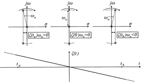
jo
jco
4(ta)(Oo>0 4'(0)wo=0 C(t)w<OM
-.
t b t
Figure 2-2: Time-varying pole/zero locations for an SRA as the damping function changes.
2.2.2
SRAs
as
Time-Varying, Second-Order Systems
An SRA differs from a linear time-invariant (LTI) system in that its poles are period-ically shifted between the left-hand side and right-hand side of the complex plane by varying the damping function ((t). The exact function used to define ((t) determines the characteristics of the SRA's response to an input signal, and various functions can and have been used [21], [66]. As an example, Fig. 2-2 shows the instantaneous value of the poles of an SRA as ((t) is linearly varied during one cycle using a ramp function. As will be shown, for each period, the resulting time-varying system yields a filtered and amplified sample of its input signal's envelope. Unlike LTI systems whose filtering qualities are strictly dependent on the static location of their poles and zeros, the filtering qualities of SRAs additionally depend on the characteristics of the damping function used to vary their pole locations. Furthermore, in contrast with LTI systems, SRAs exploit the instability portion of their cycle to achieve very high gain despite using active components that provide relatively small gain.
2.2.3
General SRA Solution for Linear Mode Operation
Historically, SRAs have been used in either the linear or logarithmic mode [44,71]. In the linear mode, the SRA is configured such that its output remains small enough throughout each quench cycle to prevent significant nonlinearities. As a result, the envelope of the SRA's output is proportional to the amplitude of the input signal. In the logarithmic mode, the SRA is configured such that its output saturates during each cycle. The integral of its envelope is then proportional to the logarithm of the input signal's amplitude. The following analysis is valid for the linear mode, but later discussions will show how the results can be used to accurately model an SRA that is allowed to enter compression.
Using (2.6) we can write the following differential equation to describe the LTV model of the SRA in Fig. 2-1
v"(t) + 2((t)wov'(t) + wov0(t) = 2R(owoi'(t). (2.8)
A more general version of (2.8) and its thorough solution can be found in [44], where the general solution is broken down into the sum of the free response and the forced response. The following analysis assumes that the free response is zero. In a practical implementation, this means that any oscillation from a previous cycle is quenched before time ta when a new cycle begins. This simplifies the mathematics, but more importantly, it improves the performance of the receiver since it ensures that each cycle is independent of all previous cycles. Mathematically, the quenching is done by allowing the poles to remain in the left-hand side long enough for the envelope of the output voltage to decay below the noise levels. To expedite the decay, the poles can be pushed far to the left, or equivalently, the damping function can be made a large positive value. Practically, this can be done by briefly shorting the tank as in [10], by reducing the transconductance, Gm (t), to a very low value as in [12], or by making
Gm(t) negative.
RLC-based SRA with an input current ia (t), resulting in the output voltage
vO(t) = ZIo o CA)d x i' (T)ewo f(A)dAsin[wo(t - r)]dr. (2.9)
In (2.9), ((t) is defined such that it is positive for ta 5 t < 0 and negative for 0 < t < tb as in Fig 2-2. The solution can be broken down into the time-dependent gain p(t) and the filtering term k(t)
vO(t) = Zop(t)k(t), (2.10) where p~)=e uotC(ANdA, (2.11) k(t) =
j
i(r)g(T)sin[wo(t - r)]dT, (2.12) and g(t) = ewo f C(A)dA. (2.13)The gain component pL(t) reaches its peak at t = tb and its maximum value p(tb) is referred to as the super-regenerative gain [71]. The term g(t) is referred to as the sensitivity function and has a peak value of unity at t = 0. For common damping functions it decays rapidly outside of a time window concentrated about t = 0, limiting the effect of the input signal ia (t) outside of that window. This quality will be exploited in Section 2.3 to approximate k(t) by a convolution and perform frequency domain analysis of the SRA. For slope-controlled SRAs, ((t) changes slowly enough that multiple periods of the input signal occur during the sensitivity period [71]. If ((t) changes from positive to negative abruptly, the SRA is said to be operating in the step-controlled region and has a significantly different frequency response. The subsequent analysis assumes the SRA is operated in the slope-controlled mode, which is preferable as it achieves better sensitivity and selectivity [71].
2.2.4
SRA Solution for a Ramp and Sine Damping Functions
Almost any arbitrary shape can be used as the damping function ((t) as long as it is positive for ta ; t < 0 and negative for 0 < t < tb. Two common waveforms in slope-controlled SRAs are the ramp (or sawtooth) and the sine-wave [10,21,42-44,66]. The ramp damping function proves particularly useful for analysis since it leads to Gaussian equations that have closed-form solutions. Furthermore, it achieves higher gain and has a frequency response preferable to that of sine-wave damping as discussed in this section and Section 2.3.2.
For the time span ta < t < tb, the ramp damping function has the form
((t) = -#t (2.14)
where
#
is its slope and has units of Hz. Substituting (2.14) into.(2.11) and (2.13) results in pramp(t) = eI = e, 2 (2.15) and t2 gramp(t) = e-w0 = , 7e (2.16) where 1s (2.17)has units of s/rad and is defined as the SRA time constant.
The sine-wave damping function has the form
((t) = -- sin(qt) (2.18)
Wq
where
Wq 2 r (2.19)
tb ta
(2.13)
results ineit)= exp (1 2c~W , (2.20)
and
g9in(t)
=
exp ~
2 .(2.21)
To facilitate the comparison between these two damping functions, we set tb =
Ital = !Tq, where Tq is the quench period, and define the ratio
tb T
S2a, (2.22)
This allows us to make the substitution Wq = 7r/(yo.). Using (2.22) and solving
(2.15) and (2.20) at t = tb allows us to evaluate the super-regenerative gain for both damping functions as
Pramp(tb) = e (2.23)
and
2 72
psin (tb) = e; 2. (2.24)
The ratio between the two gains is
iramp(tb) - e( (-2 eo . (2.25)
pLLin(tb)
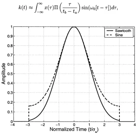
For a ratio of -y = 3, the gain of the SRA using a ramp damping function is 14.5x greater (23dB) compared with the sine-wave damping function. Of course the ampli-tude of the sine-wave damping function could be increased to increase its gain, but this would widen the bandwidth of the SRA, increasing noise and degrading selectiv-ity. This will be shown in Section 2.3.2 along with the effects of -y on the frequency response of the SRA. Fig. 2-3 shows gramp(t) and g8i,(t) for y = 3. For time
val-ues near zero, the two sensitivity functions are similar. However, gramp approaches
zero more quickly and is reduced to 0.01 at tb = 3o-, while gin is only reduced to 0.161. Later sections show this gives the ramp damping function a superior frequency
fre-quency response improves. For a given value of o-,, this requires longer quench cycles and, therefore, lower bit rates creating a tradeoff. The tradeoff favors increasing y, however, since the gain grows as e12 whereas the bit rate is reduced linearly.
2.3
Convolution Model of SRA Solution
In this section, we show that (2.12) closely resembles a convolution and exploit this quality to perform frequency domain analysis on the SRA. Typically, we are interested in the value of the envelope of v0 (t) near the end of the cycle (t ~ tb), since that is when the maximum super-regenerative gain is achieved. Since the output is oscillatory, we are not interested in its value exactly at tb, but rather at some time near tb when the sinusoidal term is at its peak. In that time range, (2.12) can be rewritten as the nearly exact approximation
k(t) ~
J
x(r)II ( 7 ) sin(wo[t - T])dT,-oo tb - ta
(2.26)
-4 -3 -2 -1 0 1
Normalized Time (t/a)
2 3 4
Figure 2-3: Sensitivity functions for sawtooth/ramp and sine damping functions (7 =
where
x(t) = i'a(t)g(t). (2.27)
and
fl (x)= 1 if
lxi
< 1/2 (2.28)0 otherwise.
The approximation in (2.26) assumes tb e -t, a although this assumption is not
necessary and can be avoided at the expense of increased complexity by modifying the argument of 1(t). Equation (2.26) can be rewritten as the convolution
k,(t) = x(t)L (tb t
)
* sin(wot) (2.29)which is valid for time t 1 tb. Note that if the value of k(t) is desired near some time other than tb, that time instant can be substituted in the argument of U(t).
As discussed in Section 2.2.4, g(t) always has a maximum value of unity at t = 0, and typically drops sharply for |t| > 3u,. Fig. 2-4 illustrates the effects of this property on (2.12) when ia(t) is the sinusoid
ia(t) = Ia sin(wat + #a). (2.30)
As shown in Fig. 2-4(a,b), g(t) grows to a maximum value of unity as the damping function approaches zero. Fig. 2-4(c) illustrates the time derivative of ia(t), and (d) shows x(t) which has the form of a time-windowed version i'(t). As shown in Fig. 2-4(e), k(t) is oscillatory and grows for t < 3o,, but then flattens out. This occurs because x(t) becomes very small for values of t > 3-,. As mentioned previously,
k, (t) is only valid (and nearly exact) for t ~ tb. However, Fig. 2-5 shows that it is
generally a very good approximation for values of t > 3u,. In fact, if 7 > 3, (2.29) can be simplified further by removing the 11(t) term without much loss to accuracy since x(t) is very nearly zero for