HAL Id: tel-01803013
https://tel.archives-ouvertes.fr/tel-01803013
Submitted on 30 May 2018
HAL is a multi-disciplinary open access
archive for the deposit and dissemination of
sci-entific research documents, whether they are
pub-lished or not. The documents may come from
teaching and research institutions in France or
abroad, or from public or private research centers.
L’archive ouverte pluridisciplinaire HAL, est
destinée au dépôt et à la diffusion de documents
scientifiques de niveau recherche, publiés ou non,
émanant des établissements d’enseignement et de
recherche français ou étrangers, des laboratoires
publics ou privés.
Atomistic simulations of H2 and He plasmas
modification of thin-films materials for advanced etch
processes
Vahagn Martirosyan
To cite this version:
Vahagn Martirosyan. Atomistic simulations of H2 and He plasmas modification of thin-films
materi-als for advanced etch processes. Micro and nanotechnologies/Microelectronics. Université Grenoble
Alpes, 2017. English. �NNT : 2017GREAT101�. �tel-01803013�
THÈSE
Pour obtenir le grade de
DOCTEUR DE LA
COMMUNAUTÉ UNIVERSITÉ GRENOBLE ALPES
Spécialité : NANO ELECTRONIQUE ET NANO TECHNOLOGIES
Arrêté ministériel : 25 mai 2016Présentée par
Vahagn MARTIROSYAN
Thèse dirigée par Olivier JOUBERT, CNRS
et codirigée par Emilie DESPIAU-PUJO, UJF
préparée au sein du Laboratoire Laboratoire des Technologies
de la Microélectronique
dans l'École Doctorale Electronique, Electrotechnique,
Automatique, Traitement du Signal (EEATS)
Modification de matériaux en couches
minces par plasmas H2 ou He : Simulations
atomistiques pour procédés de gravure
innovants
Atomistic simulations of H2 and He plasmas
modification of thin-films materials for
advanced etch processes
Thèse soutenue publiquement le 15 décembre 2017,
devant le jury composé de :
Monsieur Olivier JOUBERT
Directeur de Recherche, CNRS, Directeur de thèse
Monsieur Remi DUSSART
Professeur, Université d'Orléans, Président
Monsieur Jonathan MOUGENOT
Maître de Conférences, Université Paris 13 , Examinateur
Madame Emilie DESPIAU-PUJO
Maître de Conférences, Université Grenoble Alpes, Co-directeur de thèse
Monsieur Vasco GUERRA
Professeur, IST Lisbonne, Portugal , Rapporteur
Monsieur Gilles CARTRY
1
Table of abbreviations ……….……… 4
1. General introduction ……… 5
1.1. The evolution of Microelectronics ………. 6
1.2. Low-temperature reactive plasmas ……….. 9
1.2.1. Structure of radio-frequency (RF) glow discharges ……… 10
1.2.2. Plasma sheath and directional ion bombardment ………. 12
1.3. Low-pressure plasmas for material processing in Microelectronics ………. 14
1.3.1. Surface reactions and Etching mechanisms ……… 14
1.3.2. How to transfer a pattern into a material stack? ……… 15
1.4. Technological challenges of advanced plasma etching processes
for next-generation transistors ……….. 18
1.4.1. Structure of advanced transistors (FinFET and FDSOI) ……….. 18
1.4.2. Limitations of conventional plasma processes (CW-ICP and CCP) ………. 21
1.4.3. Alternative plasma technologies for advanced etching processes ……… 25
1.5. Light gases (H
2/He) material modification for nanoscale precision etching .…..…….. 29
1.5.1. The Smart Cut
TMtechnology for SOI substrates preparation ……….. 29
1.5.2. The Smart Etch concept ………. 30
1.5.2.1.
Principle of the Smart Etch ……….. 31
1.5.2.2.
Experimental implementation of the Smart Etch concept ………… 32
1.6. Molecular Dynamics simulations to assist process development ………. 35
1.7. Purpose of the study and organization of the PhD manuscript ………. 36
2. Molecular dynamics simulations ……….. 38
2.1. MD: General principles ……… 39
2.1.1.
Atomic motion ………. 39
2.1.2. Interatomic potentials, ab-initio and classical MD ………. 40
2.1.3. Statistical physics ……… 41
2.1.4. Numerical integration ………. 41
2.2. MD for modeling plasma-surface interaction ………...……. 42
2.2.1. General concept of the model ………...……. 43
2.2.2. Simulation of plasma species impacts ………...…… 43
2.2.3. Simulation cell and periodic boundary conditions ………. 44
2.2.4. Thermalization ………. 45
2.2.5. Timescale related problems ……… 46
2.2.6. Etch products ……… 47
2.3. Modeling of Si-H-He and SiN-H-He interactions ……… 48
2.3.1. Choice of the Si-H interatomic potential ……….. 48
2.3.2. Choice of the Si-N-H interatomic potential ………. 48
2.3.3. Choice of the Si/SiN-He interatomic potential ………..…….. 49
2.4. Preparation of the initial Si and SiN substrates ………. 49
2.4.1.
Crystalline Si (100) substrate ………..………. 49
2.4.2.
Amorphous SiN substrate ………..……… 50
2.5. Encountered issues related to H
2and He interactions with Si and SiN ………... 52
2.5.1. Timestep and cell size ……… 52
2.5.2. Adequate runtime and capture of He and H
2desorption phenomena ……….. 53
2.6. Computational details and simulation parameters ……… 56
2
2.6.2. Analysis of the substrate modification ………..….. 60
3. Helium plasma modification of Si/Si
3N
4thin films ………...………... 63
3.1. Motivation and objectives of the study ………... 63
3.2. Computational details ………..………... 64
3.2.1. Preliminary statistical studies ………...………… 64
3.2.2. Conditions of simulation ……….. 66
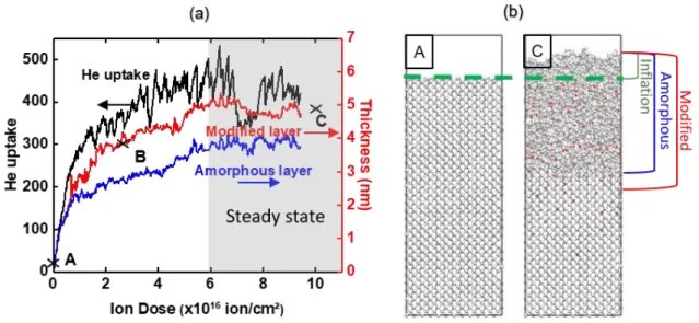
3.3. Surface evolution with the ion dose and self-limited ion implantation ………..………. 68
3.4. Structure and composition of the modified layers at steady state ………..……… 70
3.5. Helium trapping and clusters formation in both materials ………... 72
3.5.1. Mechanisms of He implantation and storage ………..………. 72
3.5.2. Temperature-dependent desorption of He ………..……….. 74
3.6. Influence of the ion energy on the substrate modification ………..……. 76
3.7. Comparison with experimental data ………....………… 77
3.8. Technological potential of helium plasmas for the Smart Etch process ………..…. 81
3.9. Conclusion ………..……….... 82
4. Hydrogen plasmas modification of Si thin films ………..…… 84
4.1. Motivation and objectives of the study ………. 84
4.2. Computational details ………... 86
4.3. H
x+(x=1-3) ion implantation in Si ……… 87
4.3.1. Surface evolution with the ion dose and self-limited ion implantation ……… 87
4.3.2. Structure of the H-implanted Si layer at steady state ………...………..… 89
4.3.3. Influence of ion type and ion energy on the substrate modification ………..….. 92
4.3.4. Effect of the surface temperature and application to the Smart-Cut technology …. 94
4.4. Mixed H
x+ion/ H radical bombardment of silicon (H
2plasma exposure) ……… 96
4.4.1. Surface evolution with the ion dose and etching ………..….. 96
4.4.2. Structure and composition of the [a-Si:H] modified layer at steady state ……….. 98
4.4.3. Influence of the ion energy (E
ion) ……….. 99
4.4.4. Influence of the radical-to-ion flux ratio (Γ= Γ
H/ Γ
Hx+) ……….. 100
4.4.5. Influence of the ion composition ……….. 102
4.4.6. Limitations of hydrogen plasmas for the Smart Etch of silicon substrates ……….. 103
4.5. Conclusion ………..……. 104
5. Modification of SiN by a H
2plasma ………. 106
5.1. Motivation and objectives of the study ……… 106
5.2. Computational details ……….. 107
5.3. Pure H
x+(x=1-3) ion implantation in SiN ……….. 108
5.3.1. Evolution of the surface with the ion dose ……… 109
5.3.2. Structure of the H-implanted material at steady state ………. 110
5.3.3. Influence of the ion energy and ion type on the substrate modification ………. 111
5.3.4. Conclusive remarks ………. 115
5.4. Mixed H
x+ion/H radical bombardment of SiN (H
2plasma exposure) ……… 116
5.4.1. Evolution of the surface with the ion dose ………..…………. 117
5.4.2. Structure and composition of the modified layer at steady state ………. 118
5.4.3. Influence of the ion energy (E
ion) ……….. 119
5.4.4. Influence of the radical-to-ion flux ratio (Γ= Γ
H/ Γ
Hx+) ……….... 121
3
5.4.6. Comparison with experiments ………..………... 123
5.4.7. Stochastic effects of ion implantation at low doses ……… 127
5.4.8. Key parameters for the Smart Etch of SiN in hydrogen plasmas ……….. 130
5.5. Conclusion ………..…….. 134
6. General conclusion ………..…….. 136
7. Appendix ……… 141
7.1. Interatomic Potentials used in the present work ………..……… 141
7.1.1. Tersoff’s potential ……….. 141
7.1.2. Murty’s Si-H potential and the simplified cubic interpolation ………..……. 143
7.1.3. ZRL Si-N-O-H potential ………..…………. 146
7.1.4. Modeling of the repulsiveness for short interatomic distances ……… 149
7.2. Straightforward way to debug the force field ………. 150
7.3. Optimization and parallelization of the MD code ………..………. 151
7.3.1. Modified re-neighboring algorithm: Smart linked cell ………...………..….. 151
7.3.2. Optimization, using atomic order ……… 154
7.3.3. Principles of the OpenMP parallelization ………..……… 155
4
Table of abbreviations
Symbol
Description
ALE
Atomic Layer Etching
ARDE
Aspect Ratio Depending Etching
CCP
Capacitively Coupled Plasma
CMOS
Complementary Metal Oxide Semiconductor
CW
Continuous Waves
FDSOI
Fully Depleted Silicon on Insulator
FET
Field Effect Transistor
ICP
Inductively Coupled Plasma
IEDF
Ion Energy Distribution Function
LTM
Laboratoire des Technologies de la Microélectronique
MD
Molecular Dynamics
MOSFET
Metal Oxide Semiconductor Field Effect Transistor
REBO
Reactive Empirical Bond Order
RF
Radio-Frequency
RFA
Retarding Field Analyzer
RIE
Reactive Ion Etching
TEM
Transmission Electron Microscopy
XPS
X-ray Photoelectron Spectroscopy
5
Chapter 1
General Introduction
1. General introduction ……… 5
1.1. The evolution of Microelectronics ………. 6
1.2. Low-temperature reactive plasmas ……….. 9
1.2.1. Structure of radio-frequency (RF) glow discharges ……… 10
1.2.2. Plasma sheath and directional ion bombardment ………. 12
1.3. Low-pressure plasmas for material processing in Microelectronics ………. 14
1.3.1. Surface reactions and Etching mechanisms ……… 14
1.3.2. How to transfer a pattern into a material stack? ……… 15
1.4. Technological challenges of advanced plasma etching processes
for next-generation transistors ……….. 18
1.4.1. Structure of advanced transistors (FinFET and FDSOI) ……….. 18
1.4.2. Limitations of conventional plasma processes (CW-ICP and CCP) ………. 21
1.4.3. Alternative plasma technologies for advanced etching processes ……… 25
1.5. Light gases (H
2/He) material modification for nanoscale precision etching .…..…….. 29
1.5.1. The Smart Cut
TMtechnology for SOI substrates preparation ……….. 29
1.5.2. The Smart Etch concept ………. 30
1.5.2.1.
Principle of the Smart Etch ……….. 31
1.5.2.2.
Experimental implementation of the Smart Etch concept ………… 32
1.6. Molecular Dynamics simulations to assist process development ………. 35
1.7. Purpose of the study and organization of the PhD manuscript ………. 36
We are leaving in the world where microelectronic devices such as smartphones, computers, cameras, sensors and many other ones, became an inseparable part of our life. These devices have evolved for the last 40 years, and will evolve as long as there is a demand. One part of this demand is surely based on the necessity of people to have more and more powerful and less expensive gadgets in their quotidian, since these devices allow to ameliorate their life. In this context, microelectronics has enjoyed an extraordinary success since its birth in the 60’s; for example, it is sufficient to say that most part of smartphones released in 2017 are much more powerful and functional than most part of computers only ten years before, and the prices are not comparable neither. However, the production of smartphones, is far from being the only field necessitating the development of microelectronics. It is even more required in the scientific environment, especially for the development of AI (Artificial Intelligence) and of numerical simulations, two fields which were born and developed alongside microelectronics, and which are nowadays coexisting as a mutual aid system. Although the performance of computing devices has increased significantly, currently it is highly insufficient for multiple simulations; therefore, the further
6
evolution of microelectronics should allow us to move faster towards the fundamental understanding of Physics (nature). Although it is easy to see the rise of microelectronics each year, one should know that there is a huge scientific, engineering and computer work behind this progress, and that each year, overcoming new technological problems becomes more and more challenging. In this thesis work, we will deal with one of these specific challenges, but in order to understand the related problems, let’s take a short review on micro-components bases and examine the tools used in their fabrication.
1.1. The evolution of Microelectronics
First, let’s start with some notions and definitions, which are unavoidable in the world of microelectronics.
A semiconductor is a material that has an electrical conductivity value falling between that of a conductor, such as copper, and an insulator, such as glass.
In other words, semiconductors are neither conductors nor insulators; however, as one can guess from the name, in some cases it can behave like a conductor, and this property is at the heart of transistor fabrication and operation.
A transistor is a semiconductor device used to amplify or switch electronic signals and electrical power.
The concept of field effect transistor (FET) was patented by Julius Edgar Lilienfeld in 1926 [Lilienfeld 26], but the first practically implemented device was a point-contact transistor, invented in 1947 by William Shockley, John Bardeen and Walter Brattain [Bell Labs]. The transistor is the building block of modern electronic devices and has revolutionized the world; its inventors worthily shared the 1956 Nobel Prize in Physics for their achievement. There are multiple types of transistors but here we focus on the most used in microelectronics: the field effect transistor. As it was mentioned, semiconductors are not conductive, i.e. there is no free charge inside these materials; however, it is possible to add electrical charges into materials via doping (using ion implantation). There are two types of doping, n and p; the first one consists in implanting additional negative charges (electrons), the other one positive charges (holes). Figure 1.1 shows an npn transistor, with a metal gate and an insulator between the substrate and the gate. When there is no voltage applied on the gate, some electrons diffuse and cross the np border, creating a barrier for the further diffusion of electrons and thus blocking the current. On the
7
contrary, when a positive voltage is applied on the metal gate, this attracts the electrons and creates a channel allowing electrons to flow through it.
Using this property, we can create two states in the transistor, OFF when there is no current, and ON when there is one, which gives a possibility to create a binary system. The magic of the transistor is the invariance regarding to its size. Since transistor operation does not depend on its dimensions, the miniaturization of components could start in the early 60’s and continue until today, which played a key role in the successful development of microelectronics. From Figure 1.1, we can understand what advantages the miniaturization brings: by reducing the size of the transistor, we hit 3 targets at a time:
• Smaller transistors are faster, since the electrons must pass a shorter distance (gate length) during the switch (ON/OFF)
• Smaller transistors are less energy consuming, since smaller transistors require lower voltage to switch
• Smaller transistors generate less material waste
The first transistor was the size of a human palm, while in December 2016, TSMC, GlobalFoundries, IBM and Samsung separately presented papers on 7nm FinFET technology [IEDM 16]. Figure 1.2 illustrates well this race to miniaturization by showing, on the left, a 5Mb hard drive produced in 1956 by IBM, and on the right, a standard current micro-SD produced in 2017, which can easily have a storage capacity greater than 256 GB. This is an illustration of the famous Moore’s law, predicted by Intel co-founder Gordon Moore in 1965, saying that the number of transistors per square inch on integrated circuits will double every year.
Figure 1.1. Example of a FET (field effect transistor). When there is no voltage applied on the gate, there is no current between the source and the drain: the transistor is OFF. When there is a positive applied voltage, there is a current flowing through the channel: the transistor is ON
8
Nevertheless, this race to miniaturization may stop soon since transistors are reaching dimensions where quantic effects are not anymore negligible, which can perturb the expected properties of micro-components.
Given the current size of advanced transistors, we understand they cannot simply be handmade, so let’s study the physics/technology allowing the fabrication of such tiny structures. Currently there are two principal ways to fabricate such micro-components, which are known as “bottom-up” and “top-down” methods. The “bottom-up” method consists in assembling the elementary (molecular or even atomic) components into a complex structure, like in the famous video-game “Tetris”. However, this approach is not highly adopted by the industry, since it is very time consuming and thus not applicable for massive fabrication. The “top-down” method is a combination of lithographic and plasma etching steps for the construction of complex material stacks. This method has always been used for the fabrication of integrated circuits; all its steps have evolved (and have been ameliorated) with time, allowing the successful miniaturization of micro-components. The role of etching in this procedure is to transfer patterns in the active layers of the transistors. Historically (until the 80’s), this step was performed using wet etching processes. They were later replaced by dry (plasma) etching processes, since plasmas allow to achieve anisotropic etching (see Figure 1.3), which is vital for the fabrication of the newest transistors, having sizes of ~10nm.
Figure 1.2.
(left) IBM 5MB hard drive in 1956, price in 1956 3200$ ~30000$ in 2017
(right) Micro-SD 256 GB in 2017, price ~100$
Price per MB is decreased more than 15 million times.
9
1.2. Low-temperature reactive plasmasPlasma is one of the four fundamental states of matter (plasma, gas, liquid, solid) and represents 99% of the matter in the Universe. Maybe the simplest definition of a plasma is as follows:
Plasma is a totally or partially ionized gas.
It is composed of stable molecules, neutral atoms, electrons and ions, but this collection of charged particles is, on average, electrically neutral. Plasmas can be classified according to their charged particle density (ne in cm-3) and their electron temperature (Te in eV). One of the most important property of
plasmas is known as quasineutrality, i.e. that the density of negative species (electrons and negative ions) is equal to the density of positive species (positive ions). As the quasineutrality suggests, a plasma is globally neutral, but not always, or more precisely, not everywhere: significant charge densities can spontaneously exist only within some distance which is known as the Debye length [Lieberman 05]. The other representative property of a plasma is its tendency to preserve the quasineutrality, which induces various plasma behaviors like the plasma oscillation. If in some region of a plasma, some part of electrons is rolled away, it creates a positive space charge region, which will attract back these electrons. In reality, this is what happens in a plasma permanently: electrons being faster tend to escape from the plasma, but are attracted back, and this process is repeating, which is known as the plasma oscillation. The frequency of this oscillation, called electron plasma frequency, is one of the fundamental characteristic of plasmas [Lieberman 05]. Plasmas can be natural (like the core of the Sun, the interstellar space, the aurorae) or artificial. Among the artificial plasmas, one can distinguish the “hot plasmas” (used for magnetic and inertial confinement fusion), the “thermal plasmas” (widely used in
Figure 1.3.
Illustration of wet (isotropic) etching and dry plasma (anisotropic) etching.
10
metallurgy) and the “cold (or low-temperature) plasmas”, used for material processing in microelectronics and which are further described below.
1.2.1. Structure of radio-frequency (RF) glow discharges
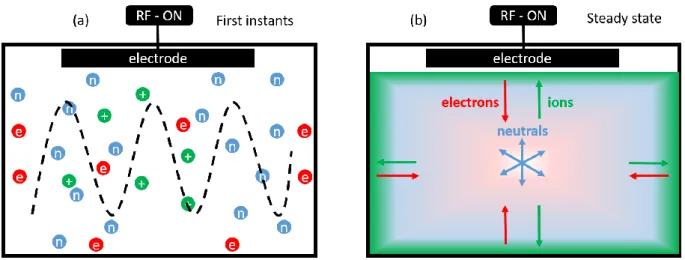
To create artificially a plasma from a gas, one should supply enough energy to ionize it. In the microelectronic industry, glow discharges are obtained by applying an electric field to a gas into a reactor. Since a gas is normally composed of neutral molecules and atoms only, this electric field should cause nothing, but as often in nature, there are some impurities in the system. In this case, there are some randomly and freely moving electrons, which can respond instantaneously to this electric field. These few electrons, which gain energy (i.e. are heated) by absorbing the electrical power, collide with other particles and can ionize them (detach an electron), initiating a chain reaction called electron avalanche.
The generation of a simple RF (radio frequency) glow discharge created in a reactor is illustrated in Figure 1.4(a,b).
The gas is confined in the reactor Figure 1.4(a), where there is an electrode contacted to a RF source, which is able to generate signals of type 𝐸 = 𝐸0+ 𝐴 ∗ sin(𝜔𝑡). Once the RF is applied, as presented in
Figure 1.4(b), free electrons are responding to this electric field, and inelastic collisions between electrons and other plasma species can accomplish any of the following processes:
Figure 1.4. Generation of a RF discharge containing neutral atoms (blue), electrons (red) and positive ions (green). (a) RF is OFF, there are few free electrons, (b) RF is ON which starts the electron avalanche and turns on the plasma.
11
• Excitation: 𝐴 + 𝑒 → 𝐴∗+ 𝑒; 𝐴∗→ 𝐴 + ℎ𝜈
𝐴. The electron impact excitation is responsible for the
glow and the color of plasma discharges.
• Dissociation: 𝐴2+ 𝑒 → 𝐴 + 𝐴 + 𝑒. This process converts relatively unreactive etch gas
molecules into chemically reactive radicals, often used as precursors in deposition or etching mechanisms.
• Ionization: 𝐴 + 𝑒 → 𝐴++ 𝑒. This process is indispensable to maintain the plasma and is the
most energy-requiring one. It takes place for all type of elements but for different electron energy thresholds. The most resistive gas vis-a-vis to ionization is helium, which needs 24.7eV to release an electron. It is also possible to have a dissociative ionization 𝐴2+ 𝑒 → 𝐴 + 𝐴∗+ 𝑒. • Attachment: 𝐴 + 𝑒 → 𝐴−. Although negativeions do not play a direct role in material processing,
this process should not be underestimated. Indeed, it is usually favored compared to ionization and the presence of negative ions can modify the plasma properties (sheaths, ion flux, etc.). Often this process occurs alongside with molecule dissociation.
Glow discharges are driven/sustained electrically and can be excited at various frequencies (DC or low-frequency, RF, microwave). Plasmas used for etching or deposition are often driven at frequencies lying between 1MHz and 200MHz, i.e. within the radiofrequency (RF) domain. In particular, 13.56MHz and its harmonic are standards which have been set aside for industrial applications. Indeed, since the masses of ions and electrons are very different (e.g. H+ ions are 1836 times heavier than electrons in a
hydrogen plasma), in the RF range, these species react very differently to the electric field: electrons being very mobile follow the instantaneous variations of the electric field, meanwhile the ions respond only to its time-average value. For very low frequencies, ions could follow the electric field as well, and vice versa, for very high frequencies, electrons would stop do it. This distinct behavior rises an exceptional property of RF glow discharges: each type of species is in thermal equilibrium with itself, meanwhile they are not in equilibrium with each other. In particular, due to the weak energy coupling between electrons and heavy particles (𝑚𝑒≪ 𝑚𝑖,𝑛), the temperature of electrons is much higher than
12
1.2.2. Plasma sheath and directional ion bombardment
Since the plasma is enclosed in a reactor chamber, there is a flux of particles towards the walls. This flux is given by the formula Γ = 1
4. 𝑛 ∙ 𝑣𝑡ℎ, where 𝑛 is the particle density and 𝑣𝑡ℎ is the thermal velocity
of particles and can be computed as 𝑣𝑡ℎ= √ 8𝐾𝑏𝑇
𝜋𝑚, where T is the temperature of the species and m is
its mass. Since 𝑇𝑒≫ 𝑇𝑖 and 𝑚𝑒≪ 𝑚𝑖, thus Γ𝑒≫ Γ𝑖. This means that the plasma should lose electrons
faster than ions, which is impossible at steady state since in this case the plasma would not remain quasineutral. Thus, the flux equality Γ𝑒= Γ𝑖 must be fulfilled, but how? In the first instants of plasma,
when switching the discharge, electrons are favored to go to the walls (see Figure 1.5(a)): after this step, which happens almost instantaneously since electrons are very rapid, a positive space charge region is created between the walls (which get negatively polarized) and the plasma. This positively charged region is called the sheath and is represented in green (the color which corresponds to ions) in Figure 1.5(a). Sheaths, which ensure that the plasma remains quasineutral, are small regions (~100µm–1cm) where substantial electric fields can develop across. Their role is to confine low energy electrons (and negative ions) into the plasma and to accelerate positive ions towards the walls. Since the flux of bombarding ions is anisotropic (parallel to the electric field) and since their energy can be tuned (by controlling the sheath voltage), sheaths are obviously interesting for surface treatment in general and in particular for etching applications. On the contrary, as illustrated in Figure 1.5(b),neutral species (atoms and molecules) are ignoring this effect and tend to diffuse isotropically towards the surfaces where they can - eventually - chemically react.
Figure 1.5. (a) First instants of the plasma, favored loss of electrons on the walls. (b) Creation of sheaths, which equilibrate the ion and electron fluxes on the walls.
13
The understanding of the sheath formation becomes more coherent when ion and electron fluxes are described quantitatively. To do that, let’s use the fact that at steady state, Γ𝑒= Γ𝑖, and solve it
mathematically for an electropositive plasma. This calculation was first done by Bohm in 1949. It was shown that when the sheath is established, on its edge the ions have a velocity Vi higher than 𝑈𝑏 = √
𝑘𝑇𝑒 𝑚𝑖,
which is known as the Bohm criteria. Often it is also interpreted in reverse: for the sheath to be established, on the edge of the sheath, ions should have a velocity at least equal to Ub. A more detailed
structure of the plasma discharge is given on Figure 1.6.
At steady state, the flux of positive ions at the walls is given by the following formula: Γi = 0.6 ∙ 𝑛0∙ 𝑈𝑏, (1.1)
where the 𝑛0 is the electron density in the center of plasma, this flux being called the Bohm flux. And
the plasma potential is given as follows:
𝑉𝑝𝑙𝑎𝑠𝑚𝑎 = 1
2𝑘𝑇𝑒∗ ln ( 𝑚𝑖
2𝜋𝑚𝑒). (1.2)
The derivation of these formulas is detailed elsewhere [Lieberman 05], nevertheless we can understand them intuitively. Since the ions are entering the sheath with the Bohm velocity, the linear dependence between this velocity and the ion flux is clear, as well as the dependence on 𝑛0, since on the sheath
edge the ion density is 𝑛0. The dependence of the plasma potential (Vplasma) on the electron temperature
(Te) is easy to understand: the higher the electron temperature, the more electrons will be lost at the walls, and thus the more positively charged the plasma will be compared to the walls. The dependence on the ion mass can be explained by the following statements. Firstly, the plasma is created and
Figure 1.6. Structure of the discharge: plasma species density (electrons, ions and neutrals) and potential profiles depending on the location. The sheath region is represented in green.
14
sustained via transformation of the electrical power (RF) into kinetic energy of electrons, a part of which is then converted into potential energy (sheath), which is afterwards dissipated by ions impinging on the walls. The heavier the ions, the smaller the Bohm flux (following the Bohm criteria). Thus, since the ion energy acquired in the sheath does not depend on the ion mass, the smaller the dissipated energy on the walls, and consequently the higher the plasma potential. The electron temperature in his turn depends on the plasma pressure and the reactor geometry. Since classically Te ~3eV, for most gases it gives about ~15eV of plasma potential, which means that the ions impinging on the walls have at least ~15eV.
Note that the nature of sheaths and plasma discharges can be much more complicated, and that here only a simplified model was given. For a more detailed description, the readers are invited to examine other works specifically dedicated to RF plasma discharges [Lieberman 05].
1.3. Low-pressure plasmas for material processing in Microelectronics
Now that the operation of a discharge is more or less understood, we can learn how it can be applied for material processing in microelectronics. The main two properties of discharges exploited in microelectronics are: the isotropic flux of radicals, and the anisotropic flux of energetic ions towards the walls.
1.3.1. Surface reactions and etching mechanisms
The main interest of discharges for surface processing lies in the reactions taking place between reactive radicals or ions present in the plasma, and the substrate atoms. Particularly, reactive radicals can chemically react and create volatile products with substrate atoms (which then move back into the plasma), which is known as chemical etching. A classic example of such reaction is the etching of silicon by halogens (Cl, F, Br), where the formed volatile products are mainly in form of SiX4, where X
represents the radical used in the process. These reactive radicals may also allow to etch one material selectively with respect to another one, since they do not react similarly with all type of atoms. With an appropriate choice of plasma chemistry, for example, one can stop the etching of a specific thin layer when the underlying material will be reached. However, chemical etching remains perfectly isotropic, meanwhile one big advantage of dry plasma etching is the ability of anisotropic (directional) etching. This specific ability comes from the plasma ions, which are able to sputter substrate atoms, which is known as physical etching. Ions are indeed accelerated towards the surface, and mostly promote the
15
vertical etching. The role of impacting ions on etching anisotropy is very complex and is very case-dependent. Particularly, depending on the ion type, the ion energy or the targeted material, the mechanisms of how ion bombardment promotes the anisotropic etching are very diverse. The most distinguishing property of physical etching is its ability to etch non-volatile products. In some processes, the effects of only one of these two plasma species (radicals or ions) may be wanted. Yet in classical ICP/CCP plasmas (see section 1.4.2 for details), we deal with the combination of these two effects known as RIE (Reactive Ion Etching). RIE is not a simple combination of two etching mechanisms, but a synergy between them, which yields quite new properties. Particularly, the resulting etch rate (i.e. the speed of etching) may be much faster than the sum of each mechanism etch rate taken apart [Coburn 79]. Of course, the fundamental interpretation of this ion-neutral synergy is quite complex and case-dependent, which is one of the reasons of empirical research in microelectronics.
1.3.2. How to transfer a pattern into a material stack?
It may be a bit sophisticated to enter directly in the application of plasma discharges for the fabrication of new type of transistors, so here we just study some elementary bricks, which are implied in such processes, and only in abstract forms, to preserve the genericity.
Example 1. Imagine that we have a substrate of element A, and we want to remove few nanometers of this material from the top (see Figure 1.7(a)). We place the substrate above the electrode in the discharge chamber, and we use a plasma which is able to etch material A.
In this case the material will be etched via RIE, and to remove the given thickness from the top, it is sufficient to estimate the etch rate, and compute the necessary plasma exposure time.
Example 2. Now let’s imagine that we have a substrate of element A, and we want to add few nanometers of element B upon the first one (see Figure 1.8(a)). In this case, a method named CVD (chemical vapor deposition) is often used, which has numerous variations, like LPCVD (low pressure
16
CVD), UHVCVD (ultra-high vacuum CVD), etc. But let’s consider here a deposition technique which implies a plasma, i.e. the PECVD (plasma enhanced CVD). One should thus take a plasma containing the element B (see Figure 1.8(b)), and place the substrate above the electrode in the discharge chamber.
In this process, the main role is played by radicals (chemically active), which will continuously bind to the dangling bonds of the substrate, allowing element B to progressively grow upon element A.
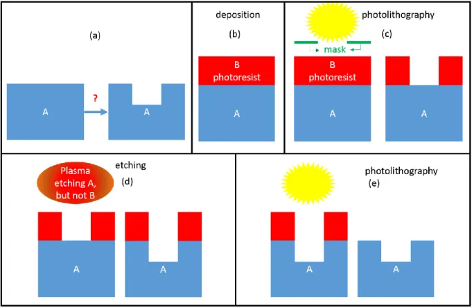
Example 3. Finally, consider a much difficult process implying more steps. Let’s try to create a pattern in a substrate (see Figure 1.9(a)). In the first step (Figure 1.9(b)), a photoresist is deposited on material A. A photoresist is a light-sensitive material, which degrades when it is exposed to light emission, and then the degraded part is easily removed using an appropriate chemistry. Then, using a mask, we create a pattern in material B (Figure 1.9(c)). Afterwards we proceed to the etching step, where we choose a plasma chemistry that can etch material A but cannot etch material B (selective etching), in order to etch only the part where A is not protected by B (Figure 1.9(d)). Finally, we remove the photoresist by degrading it via light emission exposure (Figure 1.9(e)). From this simple example, we can evoke a lot of technical problems involved in this process and encountered in real experimental conditions, but let’s consider only those that are related to the etching.
17
As seen in Figure 1.9(e), after the etching step the pattern has a perfect rectangular form, i.e. the etching was faultlessly anisotropic. This is almost impossible in practice, since among the species impinging on the substrate, only ions have a normal incidence (anisotropic flux). Since reactive radicals are coming isotropically, they tend to induce a lateral etching, which in this case can create some undercutting feature like in Figure 1.10(a), which may in turn affect the properties of micro-compounds.
Another problem, known under the name ARDE (aspect ratio dependent etching), is illustrated in Figure 1.10(b), where the rate of lateral etching decreases with the increase of the aspect ratio (ratio between the depth and width of the pattern). One of the reasons for such a behavior is simply the fact that the
Figure 1.9. Creation of a pattern into the substrate, using deposition, photolithography and plasma etching.
Figure 1.10. Pattern transfer related problems. (a) Isotropic etching
18
radicals tend to reach more and more difficultly the bottom when the depth increases, since their flux is isotropic.
In this subsection, some simple and generic examples of pattern transfer by etching were shown, to give an idea about the goals in micro-fabrication and the encountered problems. However, in the microelectronics industry, problems are usually less abstract, since each small parameter may change crucially the problem (e.g. gas chemistry, reactor geometry, plasma source, substrate material, temperature, etc.), which turns micro-fabrication processes into a complex combinatory problem. 1.4. Technological challenges of advanced plasma etching processes for next-generation
transistors
For the development of new type of transistors, like the FinFET or FDSOI (Fully Depleted Silicon on Insulator), there is a necessity to etch complex material stacks with a nanoscale precision and an almost infinite selectivity to preserve the electronic properties of active layers (e.g. silicon channel). To understand this necessity and where it comes from, one should first know the general structure of these advanced transistors.
1.4.1. Structure of advanced transistors (FinFET and FDSOI)
In Figure 1.11(a) is illustrated the structure of a standard MOSFET (Metal Oxide Semiconductor Field Effect Transistor),
Figure 1.11. (a) Structure of a 2D planar MOSFET, (b) Structure of a 3D FinFET. The wall of the gate is set transparent, to allow to see the channel.
19
which was the main structure of transistors manufactured until 2012. Their dimensions were reduced over 40 years, but these transistors, also known as planar 2D transistors, finally met their limits in the race of miniaturization. Indeed, because of the transistor shrinking, the length of the gate decreased as well. This led to reduce the control the gate exercises over the channel region, and in particular, the leakage current became more and more problematic.
To overcome the discussed issues, numerous researches were launched in the 2000s. One possible technology making possible to solve these problems and allowing to preserve existing manufacturing processes was the FDSOI. It is represented schematically on Figure 1.13(b). The difference compared to a standard planar transistor is simple: firstly, an ultra-thin layer of insulator is placed above the silicon bulk, which is called BOX (buried oxide), and then a very thin layer of silicon film plays the role of the channel. Thanks to its thickness, there is no necessity to dope the channel, thus making the transistor fully depleted.
As it is illustrated on the Figure 1.12, this simple modification highly reduces performance-degrading leakage currents [STMicroelectronics], since the current is confined in this case. Even if this technology was used by numerous companies like IBM, TSMC and STMicroelectronics, currently only the last one continues to support it. The other companies have migrated to the development of new 3D FinFET transistors proposed by Intel.
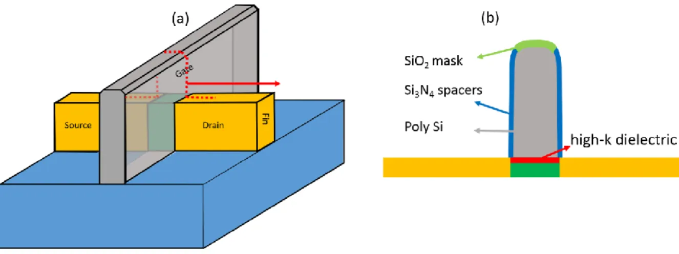
In the 2000s, University of California (Berkeley) researchers proposed a new design of transistors, known as FinFET (Fin Field-Effect Transistor) or 3D transistor, which is presented in Figure 1.11(b) (channel in green) [Chenming 00, Hisamoto 00]. In this case, the gate electrode has an excellent control over the channel because it surrounds the channel, which allows to reduce more the gate length. These transistors are already manufactured and can be found in recent products of various companies, like Intel, AMD, NVIDIA, etc. Figure 1.13(a) shows a simplified version of this modern transistor but does not give its complete structure; indeed, each brick inside is in fact covered by specific thin layers, which
20
are necessary to preserve the high functionality of the scheme. In Figure 1.13(b), the cross-cut of a FinFET is shown, where we can see the gate, a Poly-Si surrounded laterally by silicon nitride spacers and covered on top by a silicon dioxide mask. Notably, these silicon nitride spacers allow to insulate the leakage current, and their use is very common in the design of advanced transistors (e.g. in FDSOI it is used for the same purpose).
To obtain such a structure, first silicon nitride is deposited all over the surface; then it is etched anisotropically, leaving the silicon nitride spacer only on the vertical sidewalls of the gate, as illustrated in Figure 1.14.
These spacers are only few-nanometers-thick, and their removal should be done very cautiously to avoid any damage on the underlying Si, which could affect the electrical properties of the transistor. This specific etching step is a tough challenge, which is at the heart of this PhD work. It is discussed in the next subsections alongside with the limitations of conventional plasma processes.
Figure 1.13. Cross-Cut of a FinFET, which shows some thin layers present in the transistor
21
1.4.2. Limitation of conventional plasmas processes (CW-ICP and CCP)
Plasma reactors must meet high requirements in terms of etching (high etch rate, anisotropy, selectivity, uniformity, etc.) while supporting increasing substrate sizes. In addition to the chamber geometry and the excitation frequency, it is the coupling mode of the electric power to the plasma which differentiates them most. In the microelectronics industry, two types of RF sources are mainly used: the CCP (Capacitively Coupled Plasma) and the ICP (Inductively Coupled Plasma).
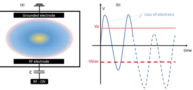
CCP reactors were the first ones used for the RIE in the 1970-1980s. The schematic of a CCP is shown in Figure 1.15(a). It is generally a parallel plate reactor, in which a plasma is confined between two electrodes, where one of them is coupled to a RF power through a capacitor, and the other one is grounded.
As it was discussed above, the minimal ion energy in such plasmas is about 15-20 eV, which corresponds to the plasma potential, but often much higher energies are required in etching procedures. In a CCP when the RF is switched ON, the plasma, aiming to keep the quasineutrality, will respond instantaneously. It will lose a lot of electrons, which will go on the upper plate of the capacitor and will charge it negatively, which in turn will shift down the RF voltage on the powered electrode below the plasma potential Vp (see Figure 1.15(b)). Ions, due to their inertia, will only see the mean voltage, also called the self-bias voltage: -Vbias. Thus, in order to increase the ion energy on the wafer, one should
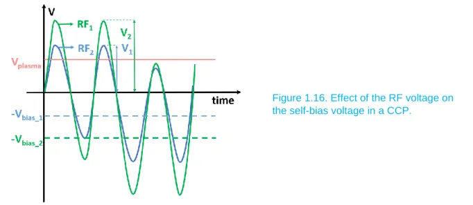
simply increase the RF power; the voltage on the powered electrode will be shifted down one more time, Figure 1.15. (a) Structure of a CCP reactor, (b) Evolution of the voltage on the RF electrode when the plasma is switched ON.
22
and the mean value -Vbias will be lower (see Figure 1.17). Since the power is coupled capacitively to the
plasma, the increase of the RF power will also increase the ion flux. Thus, CCP reactors allow to control the ion energy and the ion flux, but they do not allow to control them independently, which is an important limitation of these plasmas. This problem was overcome in the next generation of dual-frequency CCP reactors, where the RF is applied on both electrodes, but with different frequencies. In this case, the low frequency electrode controls the ion energy by modulating the RF power, while the high frequency electrode controls the plasma density by modulating the RF frequency. Working at moderate pressure (10mTorr to 1 Torr), such reactors however provide relatively low plasma densities (109-1010 cm-3) and
high ion energies (100’s of eV).
Much higher density plasmas (HDP) working at very low pressure (<10mTorr) became available thanks to the ICP reactors, in which the power is coupled inductively to the plasma via antennas (see Figure 1.17).
Figure 1.16. Effect of the RF voltage on the self-bias voltage in a CCP.
23
The variation of the RF current in the external coil (separated from the plasma via a dielectric window) induces a varying axial magnetic field, which in turn generates an azimuthal electric field accelerating electrons in the plasma. The excited electromagnetic wave is absorbed in the plasma over a characteristic length called the skin depth, large compared to the sheath size but comparable to that of the discharge. The power transfer is thus efficient and allows to achieve high plasma densities (1010
-1012 cm-3). And the higher the power on the RF coil, the higher the plasma density, and thus the higher
the ion flux on the walls. A second RF generator is connected to an electrode immersed in the plasma (capacitively coupled to the wafer), which allows to accelerate the ions toward the electrode surface with the desired energy, and to have an independent control of the ion flux and the ion energy. ICP reactors permit to obtain plasma densities/ion fluxes an order of magnitude higher than in CCP reactors. Nevertheless, these CCP and ICP reactors have a common limitation: they provide ion energies at least equal to ~15eV, which induce surface damages on a few nanometers during and after the etching [Brichon 14]. Mainly this damage is brought by the energetic ions, which can break the covalent bonds of the substrate, leading to the creation of dangling bonds inside the substrate and to the formation of diffusion paths. Often the ion bombardment amorphizes the crystalline structures [Wei 84, Vallier 99, Tuda 01, Vitale 03, Fukasawa 11], which can affect the electrical properties of thin layers. Moreover, chemically reactive plasmas lead to the formation of mixed layers near the surface [Brichon 15], which can compromise the etch precision. Another limitation of CW-ICP plasmas is the high plasma
Figure 1.17. Structure of an ICP reactor. The RF power applied on the coil is used to generate and maintain the plasma, and the RF applied on the electrode is used to accelerate the bombarding ions toward the walls.
24
dissociation rate, which induces high fluxes of radicals on the wafer and thus highly increases the etch rate. As a result, even the control of the etched thickness becomes very challenging. The discussed limitations constitute a serious problem for thin films etching, as illustrated on the following example of SiN spacers etching in FDSOI.
FDSOI - Etching of silicon nitride spacers
The fabrication process of FDSOI transistors implies several steps. In particular, the etching of silicon nitride spacers must be achieved with a nanoscale precision, in order to stop precisely on the crystalline silicon channel, as illustrated on Figure 1.18. Indeed, the underlying silicon layer must remain undamaged (structurally and chemically) to preserve its initial electrical properties and be compatible with the upcoming epitaxial steps. The CH3F/O2/He chemistry, often used in this step, is however not
consistent with these requirements.
It was shown that using a CW-ICP, a mixed SiOxFy layer is forming in the silicon channel [Blanc 14], as
illustrated on Figure 1.19.
Figure 1.18. Etching step of silicon nitride spacers for the fabrication of FDSOI transistors.
Figure 1.19. Formation and diffusion of a mixed layer (fluorinated and oxidized) in the underlying stacks during the etching step of silicon nitride spacers using a CH3F/O2/He chemistry.
25
As one can see on Figure 1.19, a mixed SiNOxFy layer is initially created in the silicon nitride surface. It
is then continuously transferred towards the subsequent layers, and finally it is merged with the crystalline silicon channel, forming a few-nanometers-thick (3-5nm dependent on the bias power) SiOxFy
mixed layer. Even if this layer can be eliminated using a HF bath, it was shown that this process causes a serious consumption of silicon, also named “silicon recess”. From this example we see that continuous-wave ICP or CCP processes are not acceptable for several fabrication procedures, where thin films etching is implied. The next subsection speaks about alternative plasma technologies allowing to overcome these issues.
1.4.3. Alternative plasma technologies for advanced etching processes
The major issue of conventional CCP and ICP plasmas for ultrathin layers etching is the relatively high ion bombardment energy (>15 eV) reaching the substrate. In this subsection, we discuss alternative plasma processes, which allow to decrease the incident ion energy. To achieve such a goal, one solution is to lower the electron temperature (Te) of the plasma, temporally (by pulsing the plasma) or spatially (by segregating the electron heating region far from the wafer).
Pulsed plasmas
Conventional ICP plasmas are often called CW-ICP (continuous wave ICP), which means that the RF source power is continuous; in pulsed ICP plasmas, the source power can be modulated temporally. The procedure is very simple: the RF power coupled to the coil is switched consecutively ON and OFF, which gives two additional parameters to control the plasma, the frequency f = 1/(tON + tOFF), and the
duty cycle DC = tON/(tON + tOFF), where tON and tOFF are the periods when the RF power is ON and OFF,
respectively. Pulsing the plasma allows to have an augmented control over the incident ion energy distribution, the plasma dissociation, the electron temperature and other parameters. When a frequency of pulsation ~1kHz is chosen (tON + tOFF ≈ 1ms), since electrons are extremely mobile and the electronic
temperature Te evolves on timescales of about 10 µs, during most of the OFF period, Te is about zero
(see Figure 1.20(a)). The decrease of Te decreases the plasma potential Vp, which decreases in average
26
Also, since the plasma dissociation is induced by electron inelastic collisions, it mostly takes place during the ON period meanwhile recombination takes place permanently. As a result, the pulsed discharge is on average less dissociated and its chemical reactivity can be controlled with the duty cycle. Like the RF source power, the bias power can be pulsed as well, and synchronized or not with the source power, which yields various combinations of pulsing mode. However, pulsing the bias power only is usually not interesting to minimize the ion energy, because in that case the ion energy will be higher than 15eV anyway.
Low-Te plasmas
Since the key parameter to reduce the ion energy is the electron temperature, new plasma reactors were developed in the 2010s to reach this goal, in particular by TEL (Tokyo Electronics Lim.). In these plasmas, the electron temperature is lowered spatially, by segregating the electron heating region far from the wafer. Different types of sources exist. One of them consists in inserting a negatively charged grid (at a constant potential)in a classical ICP, some centimeters above the electrode, which divide the plasma in two regions (see Figure 1.21(a)).
Figure 1.20. (a) Evolution of the ion flux and electron temperature when pulsing the plasma [Lieberman 96]. (b) Measured ion energy distribution functions for different duty cycles in pulsed Cl2-based plasmas [Brihoum 13].
27
The grid, located a few centimeters above the substrate, decreases the electron temperature in Region II. Indeed, Region I remains a classical ICP, meanwhile the electrons generated in Region I and which diffuse in Region II, obtain the energy imposed by the potential difference between the grid and the plasma potential in Region II. There, most electrons lose their energy by inelastic collisions, while those with high energy escape rapidly at the reactor walls. As a result, the electron temperature in Region II is less elevated [Hong 99] and can be modulated (like the electron density) by the polarization of the grid [Ikada 04], as shown in Figure 1.21(b)
E
lectron temperatures lower than 1 eV can be obtained, which is two to three times lower than electron temperatures in conventional ICP plasmas.Atomic Layer Etching
Finally, Atomic Layer Etching (ALE) is a third technique (or concept) for removing ultrathin layers of materials using sequential reactions steps that are self-limiting [Kanarik 15]. It consists in alternating several steps (deposition/passivation, purging, etching/desorption, etc.) in order to remove only one atomic layer of a substrate. This sequence of steps (or cycles) is repeated several times to perfectly control the etching of a given material (see Figure 1.22).
Figure 1.21. (a) Structure of a low-Te plasma [Bai 07]. (b) Electron temperature and density as a function of the grid (inserted in the plasma) polarization [Ikada 04].
28
Although such a concept is promising to etch sub-nm-thick stacked materials,experimentally, it is often impossible to damage only one atomic layer. Moreover, another problem remains in the extremely low etch rate, which can be achieved using several alternating steps. Thus, the ALE concept cannot yet provide sufficient productivity on an industrial scale and requires additional development to become commercially viable.
The two previous discussed techniques (pulsed and low-Te plasmas) propose a way to reduce the incident ion energy (< 15 eV) and to control the plasma reactivity, which is so necessary for ultrathin films etching, but yield other problems limiting their promises. Pulsed plasmas indeed permit to reduce the ion-induced damage (i.e. the mixed layer thickness) but not to eliminate it completely; surface damage of the order of 1nm can still be observed [Petit-Etienne 10], and besides, this method is not self-limited. Low-Te plasmas tend to deposit low-energy ions in polymerizing chemistries and to generate broad ion angular distributions, which affects the directionality and the uniformity of the etching [Kanarik 12]. Of course these limitations do not mean that such plasmas are useless - currently these techniques are used in the industry - but alternative approaches may be needed to overcome the aforementioned issues. As one can also remark, new etching processes aim to reuse the existing plasma technologies, only with tiny modifications to solve a given problem. This is not done haphazardly, because all described plasma sources are very expensive, and a completely new technology would require a replacement of existing reactors. Moreover, each of these reactors (CCP, ICP) were studied during dozens of years due to the complex physics related to their structure and geometry, and any new architecture would require such studies likewise, and consequently would be both time and money consuming. In this context, a new approach was recently proposed by Posseme et al. for silicon nitride spacer etching [Posseme 14, Smart Etch patent 14], that we will call the Smart Etch technique. It implies only conventional plasmas: in a first step, the film is modified in volume by exposition to a H2 or He CCP
29
or ICP; in a second step, the modified layer is selectively removed by wet cleaning or exposure to gaseous reactants only (downstream plasma). But before detailing this procedure, let’s examine why and how hydrogen and helium plasmas are used in microelectronics.
1.5. Light gases (H2/He) material modification for nanoscale-precision etching
Hydrogen in its monoatomic form is the lightest and most abundant element in the universe, constituting roughly 75% of all mass; the second one is helium, representing about 24% of all mass. These two ubiquitous elements have plentiful applications in very different branches of Science, from biology to nuclear physics. Their use has not been avoided in Microelectronics either, where they are present in various steps of microfabrication, especially hydrogen. At standard temperature and pressure, hydrogen is a diatomic gas (H2) which can be dissociated in chemically reactive H radicals using a plasma source.
On the contrary, helium (He) is a monoatomic and inert gas, which cannot form covalent bonds with other atoms. These two elements, which differ mainly by their chemical reactivity, have exceptional properties due to their small size and low weight (mH = 1.008u; mHe = 4.003u), and can modify materials
on a considerable depth with a high precision. One of their first applications in Microelectronics was the Smart CutTM technology.
1.5.1. The Smart CutTM technology for SOI substrates preparation
The fact that hydrogen can penetrate deep in a material and transform it was first observed in tokamaks, where H2 plasmas are used for thermonuclear fusion and where deformations of walls were observed
[Das 76]. In 1994, Bruel et al. [Smart Cut patent 94] from CEA-Leti found an excellent application to this phenomenon, named Smart Cut, for the preparation of SOI (silicon on insulator) substrates. The Smart Cut technology,based on light ions implantation and wafer-bonding, is a multistep process which allows to transfer a thin layer of crystalline material from a donor substrate to another substrate (see Figure 1.23). First, hydrogen ions are implanted in a substrate A, inducing the formation of a weakened layer located roughly at the mean ion penetration depth. Afterwards, the implanted wafer A is flipped around
and bonded to a stiffener (wafer B). Then a heat treatment phase (or annealing step) results in the cleavage of the weakened layer, allowing to separate the new thin film and the initial bulk material [Smart Cut patent 94]. In the case of SOI, the initial or donor substrate is a thermally grown silicon oxide on silicon, and the stiffener is another wafer of silicon, as shown on Figure 1.23.
30
The Smart Cut procedure is mainly based on hydrogen ion implantation, but the same technique was proposed using helium implantation [Xiang Lu 97]. This technology has a wide range of applications in microelectronics, for example in the fabrication of FDSOI transistors. By enabling any thin-film materials to be transferred on top of any other materials, it could also provide opportunities in emerging fields including sensors, flexibles electronics, 3D applications, display panels and solar cells, etc. Although the full Smart Cut procedure was the subject of various studies in the last twenty years [Aspar 97, Weldon 97, Bedell 01, Moutanabbir 05], there is still a lack of fundamental understanding [Terreault 07]. For instance, as regards the first implantation step, the hydrogen profile in the substrate and the effect of the ion energy seem to be relatively well understood, but the effect of the ion dose or the form in which hydrogen is stored in the substrate remain unclear. Similarly, the annealing step of the Smart Cut and the effect of the heat treatment are not yet entirely understood. In the following section, we will see that this property of light elements (He, H) to cause interior modifications to substrates has recently found another utility in 2014, with the Smart Etch concept.
1.5.2. The Smart Etch concept
As previously discussed, conventional etching methods in CCP or ICP allow to etch materials but tend to generate ion-induced damage and mixed reactive layers of a few nanometers in the underlying substrate, which is not desirable. To solve this problem and overcome limitations of alternative methods
31
like pulsed and low-Te plasmas, an innovative approach was recently proposed, which implies two steps.
1.5.2.1. Principle of the Smart Etch
In the first step, the material to be etched is exposed to a hydrogen or helium plasma in order to modify it by light ion implantation; in the second step, the modified part is removed using wet or dry gaseous etching, as shown on Figure 1.24 for the case of silicon nitride.
From this specific example, the potential of this method may not be fully evident since one should only choose a plasma which can etch selectively SiN with respect to Si. But the Smart Etch concept has many advantages over classical plasma processes when one wants to etch with a nanometric precision. Let’s consider that we want to etch only few (2-3) nanometers of a given material. In such a case, conventional CCP or ICP processes, besides damaging the underlayers, may bring another problem, the etch precision, since often etch rates are high which makes it difficult to control the etching. The Smart Etch method makes it possible since light ions are able to modify and weaken the material on a desired depth, without etching it. Because the modified part is much sensible with respect to a given chemistry than the non-modified part, it provides a good selectivity which allows to remove only the modified layer during the second step. Another advantage of this method is the anisotropy provided by the ion implantation, which allows further directional etching. Let’s examine this specific ability for the problem of silicon nitride spacers etching in FinFET transistors, which is presented on Figure 1.25.
32
The directionality comes from the implantation step, where a standard CCP or ICP plasma is used and where ions are accelerated toward the substrate, which allows to avoid the modification of the walls. The next step indeed uses an isotropic etch method to selectively remove the modified layer, but since the material is modified anisotropically, thus it behaves like an anisotropic one. Now that the Smart Etch concept has been described, we can address its experimental implementation and examine the difficulties encountered in the real processes.
1.5.2.2. Experimental implementation of the Smart Etch concept
H2 or He CCP/ICP exposure followed by a HF bath
One way to perform a Smart Etch is to expose the substrate to a H2 or He CCP/ICP, followed by a wet
etching step in hydrofluoric (HF) acid. In this case, the substrate should be transported from the plasma reactor to the HF bath under vacuum, to avoid oxidation. This technique, normally used for research purposes like in the PhD work of Jerome Dubois [Dubois 16], may give excellent results for thin films etching [Posseme 14, Sherpa 17] but requires a smart and cautious use. Depending on the plasma operating conditions (i.e. pressure, source and bias powers, exposure time, etc.), the ion energy and the ion flux on the substrate may be different, and thus the material modification may be different as well (i.e. the thickness of the modified layer or the rate of modification, which defines the further etch selectivity between the modified and non-modified parts). So, for each plasma condition, these two plasma parameters (ion energy and ion flux) should first be determined. Then, to characterize the material modification after plasma exposure, the substrate should be dipped into a HF bath for different times and the remaining thickness of the substrate should be measured using Ellipsometry (see Figure Figure 1.25. Anisotropic etching of silicon nitride spacers using the Smart Etch method [Posseme 14].
33
1.26).
In experimental conditions, to save time, the substrate exposed to the H2 or He plasma is cleaved in
smaller parts, and each part is exposed to different times of HF bath. From these data, the etched layer thickness can be computed, which is represented by the red curve, while the slope of the red curve gives the etch rate (etched thickness/time). This sole measurement allows to determine at a time two important unknowns: the modified layer thickness and the selectivity between the modified and non-modified layers with respect to the HF bath. Once the etch rate (green curve) suddenly decreases to become constant, one can conclude that the modified layer is fully etched. Since the interface between the modified/non-modified layers corresponds to the etch rate transition point, the modified layer thickness is inferred and the selectivity can be computed as the ratio of etch rates before and after the transition. Once these surface characterization steps are done, the real process can be used. For instance, let’s imagine that for a given material and specific plasma conditions (pressure, power, exposure time), preliminary measurements showed that the thickness of the modified layer is 2nm, the etch rate is 12nm/min, and the selectivity is 10. To etch 6nm of this material, one should enchain 3 times the following cycle: plasma exposure + 10 seconds of HF bath.
The RADION prototype: H2 CCP exposure followed by a remote NF3/NH3 plasma
The RADION is a new reactor prototype developed by Applied materials, which is able to work in both CCP and downstream modes. In downstream (remote) mode, energetic plasma ions are filtered so that the wafer, located away from the ionization region, is only exposed to radical impacts. To obtain a downstream plasma, a system of ion-blocking shower is inserted in the plasma above the substrate. The advantage of a downstream plasma over wet etching (e.g. in an HF bath) is the conformity of the

![Fig. 2.6. Preparation of an amorphous silicon nitride substrate from the crystalline state, using the melting-quench method [Ippolito 11]](https://thumb-eu.123doks.com/thumbv2/123doknet/12845448.367485/53.892.166.730.100.455/preparation-amorphous-silicon-nitride-substrate-crystalline-melting-ippolito.webp)
![Fig. 2.10. Mean ion energies in helium and hydrogen plasmas, dependent on the bias and source power, measured by [Dubois 16] using RFEA](https://thumb-eu.123doks.com/thumbv2/123doknet/12845448.367485/59.892.114.787.246.494/energies-helium-hydrogen-plasmas-dependent-source-measured-dubois.webp)