HAL Id: hal-01827058
https://hal.archives-ouvertes.fr/hal-01827058
Submitted on 1 Jul 2018
HAL is a multi-disciplinary open access
archive for the deposit and dissemination of
sci-entific research documents, whether they are
pub-lished or not. The documents may come from
teaching and research institutions in France or
abroad, or from public or private research centers.
L’archive ouverte pluridisciplinaire HAL, est
destinée au dépôt et à la diffusion de documents
scientifiques de niveau recherche, publiés ou non,
émanant des établissements d’enseignement et de
recherche français ou étrangers, des laboratoires
publics ou privés.
Impact of PCM resistance-drift in neuromorphic
systems and drift-mitigation strategy
Manan Suri, Daniele Garbin, Olivier Bichler, Damien Querlioz, Dominique
Vuillaume, Christian Gamrat, Barbara Desalvo
To cite this version:
Manan Suri, Daniele Garbin, Olivier Bichler, Damien Querlioz, Dominique Vuillaume, et al.. Impact
of PCM resistance-drift in neuromorphic systems and drift-mitigation strategy. 2013 IEEE/ACM
International Symposium on Nanoscale Architectures (NANOARCH), Jul 2013, New York, United
States. �10.1109/NanoArch.2013.6623059�. �hal-01827058�
Impact of PCM Resistance-Drift in Neuromorphic
Systems and Drift-Mitigation Strategy
Manan Suri
∗, Daniele Garbin
∗, Olivier Bichler
†, Damien Querlioz
§,
Dominique Vuillaume
‡, Christian Gamrat
†and and Barbara DeSalvo
∗∗CEA-LETI-MINATEC, 17 Rue des Martyrs, Grenoble 38054, France †CEA-LIST, Gif-sur-Yvette, France
‡CNRS-IEMN, Lille, France §IEF-Paris, France
Abstract—Neuromorphic architectures that exploit emerging resistive memory devices as synapses are currently receiving a lot of interest. Phase Change Memory (PCM), in particular, is a strong candidate for such architectures. However, it suffers from a resistance-drift effect in the amorphous phase (high-resistance). In this work, we investigate the impact of resistance-drift in ‘Learning-’ and ‘Read-’ mode operation of large-scale hybrid neuromorphic architectures that use bio-inspired ‘STDP-type’ learning rules. We show that our ‘2- PCM Synapse’ approach is inherently tolerant to resistance-drift. We also present a new architecture (‘Binary-PCM Synapse’) and programming strategy based on partial-reset states of PCM devices, which strongly minimizes the impact of resistance-drift. To benchmark the two programming approaches and architectures, we perform system-level simulations on a complex visual pattern extraction appli-cation. A power consumption analysis for the two approaches is finally presented. It highlights the ultra low-power potential of PCM-based neuromorphic computing.
I. INTRODUCTION
Interest in the field of bio-inspired computational hardware has increased dramatically over the last few years. Several research groups [1], [2], [3], [4] are actively exploring neu-romorphic hardware due to its promising advantages such as low-power, high defect/variability- tolerance, and efficient handling of large scale non-linear computations. Among the different implementations of neuromorphic hardware, of par-ticular interest are the ones that exploit hybrid architectures: CMOS + emerging resistive memory (RRAM). In these hybrid
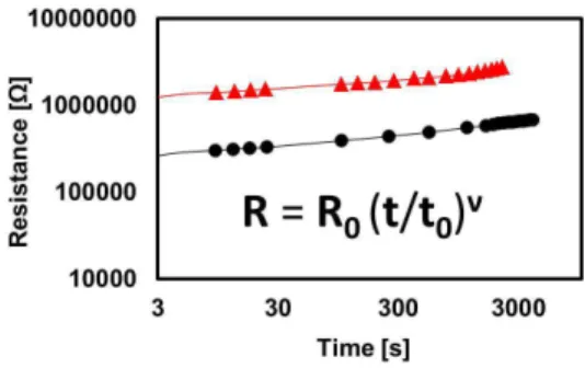
Fig. 1. Resistance drift with time for different initial programming conditions. Measurement was carried out on GST PCM devices. Equation governing the drift dynamics is also shown.
architectures, the neuronal functionality is implemented by using standard CMOS circuits while the synaptic function-ality is implemented through densely integrated arrays or crossbars of RRAM technologies. These RRAM technolo-gies may include devices such as phase change memory (PCM) [5], [6] conductive-bridge (CBRAM) or programmable-metallization cell (PMC) [4], [7] and oxide based resistive memory (OXRAM) [8], [9], [10]. Owing to their compact size, resistive-memory devices help in achieving a high synap-tic density which is not possible with pure CMOS-synapse circuits, as a large number of transistors are required (>10) per synapse [11]. RRAM also provides the much needed non-volatility to the neuromorphic system.
Here, we focus on hybrid neuromorphic architectures that use PCM devices as synapses. PCM devices consist of an active chalcogenide layer sandwiched between two metal elec-trodes. The working principle exploits reversible and non-volatile phase-change phenomena inside chalcogenide layers such as Ge2Sb2Te5 (GST). Phase-change is obtained through
joule-heating, when electrical bias or pulses are applied. PCM devices can be programmed to a high-resistance (or reset) state by creating a resistive amorphous region inside the chalcogenide layer. Heating the chalcogenide layer above its melting temperature and then quickly quenching it gives rise to formation of amorphous region. A low-resistance (or set) state can be obtained by creating crystalline regions in the chalco-genide layer. Crystallization occurs when the chalcochalco-genide layer is heated at its crystallization temperature for sufficient duration. Intermediate resistance states can also be obtained by carefully tuning the programming conditions (i.e pulse-width and amplitude) [12]. These properties have led to proposed use of PCM devices for mimicking synaptic-plasticity effects such as potentiation (LTP-like) [13], depression (LTD-like) and bio-inspired learning rules like spike-timing dependent plasticity (STDP). In previous works [6], we presented a novel low-power PCM based neuromorphic architecture called the ‘2-PCM Synapse’. Using our architecture we demonstrated a two-layer spiking neural network (SNN) capable of complex visual pattern extraction.
However, in PCM devices, the amorphous or high-resistance states are not entirely stable. Melt-quenched amor-phous regions created inside the chalcogenide layer undergo structural relaxations and the resistance of PCM device tends to increase with time (known as drift). The resistance-drift follows an empirical exponential rule which depends upon
the initial programmed resistance and a parameter known as the drift coefficient (ν) [14]. The crystalline or low-resistance states of PCM are shown to be free from resistance-drift [15]. Fig.1 shows the resistance-drift measured in our GST-PCM devices and the equation governing the drift dynamics. The devices were programmed in two different initial (reset) states and the resistance was read at different time intervals. Inside a neural network such resistance-drift may cause undesired change of trained synaptic weights.
In this paper, we discuss how our ‘2-PCM Synapse’ architecture is inherently tolerant to PCM resistance-drift. We also introduce a new ‘Binary-PCM Synapse’ architecture with a stochastic STDP learning rule. We show that by carefully defining the reset state (partial-reset) in the ‘Binary-PCM Synapse’ architecture the effects of drift can be mitigated even further. Section II describes the two different PCM based architectures and programming schemes. Section III, discusses the visual pattern extraction simulations, the impact of drift, and overall system performance.
II. PCMBASED SYNAPTICARCHITECTURES
A. The ‘2-PCM Synapse’
Our main motivation for developing the ‘2-PCM Synapse’ architecture was to emulate synaptic behavior (i.e. gradual synaptic-potentiation and -depression) using identical neuron spikes (Fig.2) [6]. In this approach, we use two PCM devices to implement a single synapse and connect them in a com-plementary configuration to the post-synaptic output neuron. One of the PCM device implements synaptic potentiation (LTP-device), while the other implements synaptic depression (LTD-device). Both devices are initialized to a high resistive amorphous state. When synaptic potentiation is required, the LTP device is crystallized, while when synaptic depression is required, the LTD device is crystallized. Fig.3 shows the characteristic resistance evolution of our GST-PCM devices with gradual crystallization events. The detailed programming schemes and the simplified STDP learning rule used are described in [6]. Note that as the neural network undergoes learning, with time the PCM devices become more and more crystallized and finally saturate to a minimum resistance value. In order to enable continuous learning of the network, we defined a refresh-sequence, explained in detail in [16]. In this
Fig. 2. Schematic of the ‘2-PCM Synapse’ architecture. Inset shows a TEM image of GST PCM device.
Fig. 3. Experimental LTP curve for pulse width of 300ns. Inset shows 100 different simulated LTP curves with a 20% standard deviation variability included on all synaptic parameters described in equation 3 of [6].
refresh-sequence, the saturated PCM devices are amorphized (reset) and the effective weights of the corresponding synapses are re-programmed.
B. ’Binary-PCM Synapse’ and Partial-Reset
Alternatively, we propose for the first time, to use PCM devices as binary synapses but with a stochastic-STDP rule, similar to the one we developed for bipolar CBRAM devices [4]. In this approach, there will be 1-PCM device per synapse. Two resistance states (or weights) can be defined for the PCM synapse. The high-resistance state should be chosen such that it is a partial-reset (Fig. 4) state. The partial-reset state should lie in the negligible or low-driftable region. For GST based devices a resistance value < 50 kΩ will lie in low or negligible drift regime [15], [14]. Fig. 5 shows an example of our stochastic-STDP rule. The y-axis represents a probability to switch from the set-to-reset or reset-to-set states for the PCM synapses. Fig. 6 shows the architecture and the programming scheme required to implement the stochastic learning with binary PCM synapses.
The stochasticity is controlled by an extrinsic PRNG (pseudo-random number generator) circuit. The PRNG circuit controls the probability of LTP and LTD with a 2-bit signal. Initially, the input neurons (A-D) generate small read pulses when they encounter any stimuli event. The read current is integrated in the output neurons A’ and B’. When the output neuron reaches its firing threshold it generates a feedback signal(3) and a post-spike signal. In the example shown in Fig. 6 output neuron A’ fires and B’ doesn’t fire. The signal(3) activates the gates of all the select transistors on the synaptic line connected to A’. If LTP is to be implemented the Input neuron will send a signal(1), as shown for Input neuron A in this example. In the case of LTD the input neuron will send a signal(2), as shown for the input neuron D. The probabilities of LTP/LTD can be tuned according to the learning rule (Fig. 5).
III. RESULTS ANDDISCUSSION
In this section, we benchmark impact of drift on the two different architectures discussed in the previous section, by
Fig. 4. Experimental Resistance-Voltage curves for different programming pulse widths on GST PCM devices.
Fig. 5. Simplified stochastic STDP learning rule. ‘On’ corresponds to set and ‘Off’ to reset of the PCM synapse.
Fig. 6. Schematic of the ‘Binary-PCM Synapse’ architecture and the proposed programming-scheme.
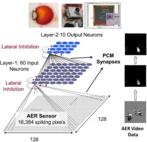
Fig. 7. (Top) Model of the retina and DVS sensor [18] used for generating AER data. (Bottom) Schematic of the two-layer SNN used for complex visual pattern extraction.
simulating a large-scale real world pattern extraction applica-tion. We used our custom built XNET SNN simulator [17] to simulate a complex visual pattern application. Our 2-layer SNN with 70 neurons and about 2 million PCM synapses is shown in Fig. 7. AER video of cars passing on a freeway was recorded using a special DVS-Sensor [18] and used as the input data for our SNN. During the learning, the neurons were able to extract patterns (car-shapes) in different lanes (different positions and orientations) in a fully unsupervised manner. The detailed learning mechanism of the network is described in [19]. Table. I and Table. II summarize the SNN performance and detection rates for all the simulations performed for this paper.
A. Drift Impact
In order to study the impact of PCM resistance-drift in our network we first classify its operation in two different modes: (a) Learning-mode and (b) Read-mode. In learning mode the synaptic programming is enabled and the network is trained using various datasets or stimuli. It is only during this mode that the synaptic weights can be changed. For the ‘2-PCM Synapse’ architecture, in the learning-mode, the PCM are typically not experiencing drift. Only, whenever a refresh-sequence is applied to a synapse, it pushes the respective PCM devices into the driftable region. In the refresh-sequence, both devices are reset and one of them is reprogrammed to a lower resistance state. For the device which stays in the fully reset state, drift is irrelevant: the more reset it is, the better. The other device, which is reprogrammed to a high resistance but intermediate state, may experience drift until it encounters sufficient crystallizing events (LTP or LTD) that push it in the non-driftable region. Such drift can delay learning, and its occurrence can be attributed to the refresh-frequency. More precisely, the drift in learning will be a consequence of the on-going competition between the refresh-frequency and the set-frequency.
Set-frequency depends on (1) nature of the learning rule and (2) nature of the stimuli used for training, while the
refresh-frequency mainly depends on the type of chalcogenide material used. A chalcogenide material which crystallizes slowly and offers more intermediate resistance states before saturation will require less frequent refresh. In previous works we showed that growth dominated materials like GeTe have almost double the refresh-frequency compared to nucleation dominated material such as GST [20]. While interface en-gineering (GST+HfO2) can further improve the number of
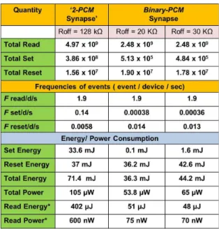
intermediate resistance states thus decreasing the refresh fre-quency [21]. From Table. I, we can see that for the ‘2-PCM Synapse’, the ratio of set-frequency (/device/s) to reset-frequency (/device/s) is about 25. In the case of interface engineered devices [21] this ratio further increases to a value of 55.
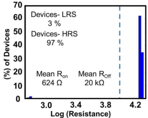
Drift is more dramatic in the case of the read-mode compared to learning mode, since the system has no means to compensate for it through learning. In the read-mode, synaptic programming is disabled and a pre-trained neural network is used to identify patterns in new datasets or stimuli without changing the synaptic weights. Thus impact of resistance-drift in the read-mode is proportional to the final weight distribution of the synapses at the end of the training, and the time interval after which the network is operated in read-mode post training. Synaptic weight distribution at the end of learning mode gives the number of synapses that are left in the high-resistance or driftable state. An inherent advantage of the ‘2-PCM Synapse’ approach, compared to the methodology used in [22], is that we implement both potentiation and depression by crystallization. Thus the majority of PCM devices at the end of the learning are programmed in low resistance or non-driftable states. This is irrespective of the fact that we use a pre-dominantly depression (LTD) based learning rule. As crystalline or low resistance states are more stable and immune to the resistance drift [14], [15], [23] the ‘2-PCM Synapse’ diminishes the loss of synaptic information in the read-mode. Fig. 8, shows the final synaptic resistance (weights) distribution at the end of the cars learning simulation. About 60% of the devices are in the non-driftable region. The strong reduction in percentage of devices in driftable region is more evident from Table. I. We can see that the number of set events is about ten times greater than number of reset events for the ‘2-PCM Synapse’ as LTD is also implemented by set or crystallization. In the case of ‘Binary-PCM Synapse’ architecture the impact of drift in learning-mode can be fully mitigated if the reset state of the PCM devices is tuned carefully to a partial-reset state (negligible drift region). Fig. 9 shows the final synaptic resistance distribution at the end of learning when the simulation was performed for the ‘Binary-PCM Synapse’ architecture with stochastic learning. In this simulation the mean reset state was defined as 20 kΩ, which lies in the non-driftable region. At the end of the learning, about 97% of the synapses are in the reset state. This is due to the strongly LTD dominant nature of our learning rule (Fig. 5). Even though majority of the synapses are in reset state, they will not drift as they lie in the non-driftable region.
We performed the cars-learning simulations for the ‘Binary-PCM Synapse’ architecture with 3 different PCM reset resistance states, keeping the set state constant: (1) negligible drift region (mean Roff = 20 kΩ), (2) Low drift region (mean Roff = 30 kΩ), and (3) high drift region (mean Roff > 100
Fig. 8. Distribution of synaptic resistance states for the ‘2-PCM Synapse’ architecture at the end of the visual learning simulation.
Fig. 9. Distribution of synaptic resistance states for the ‘Binary-PCM Synapse’ architecture with 20 kOhm mean Roff.
kΩ). The final synaptic resistance distributions for the reset devices and the set devices in the 3 cases are shown in Fig. 10 and Fig. 11 respectively.
B. Overall System Performance
Fig. 12 shows the final neuron sensitivity maps for the 6-lanes at the end of cars-learning simulation for the case of ‘2-PCM Synapse’ and ‘Binary-PCM Synapse’ (20 kΩ) architectures. Table. 2 gives the exact value of detection rate for each individual lane. Lanes 1 and 6 were classified as not-learnt as their detection rates were < 85%. The average detection rate was 91% for the ‘2-PCM Synapse’ and 95% for the ‘Binary-PCM Synapse’. Obtaining a high detection rate with an unsupervised system is a strong accomplishment from a machine learning point of view. It is also interesting that the binary synapses performed better. Binary synapses appear especially fit to process this kind of highly dynamic video data. From Table. 1 we can see that, as we move from the ‘2-PCM Synapse’ architecture to the ‘Binary-‘2-PCM Synapse’, the number of read-events becomes half as the number of PCM devices is also halved. However the read frequency/device/s stays constant. The read-frequency stays constant as it depends
Fig. 10. Distribution of synapses in off-state for the ‘Binary-PCM Synapse’ with mean Roff values of 20 kOhm, 30 kOhm and 123 kOhm.
Fig. 11. Distribution of synapses in on-state for the three cases shown in Fig.10.
on the nature of stimuli used to train the network. In the case of ‘Binary-PCM Synapse’ the set and reset events are a direct representative of the number of LTP and LTD events. However in the case of ‘2-PCM Synapse’ the reset events represent the number of refresh-sequences while the set events denote both LTP and LTD.
To estimate the energy consumption by the PCM devices during the learning process, we use the following equations (CMOS or neuron power consumption is not included):
Eset/reset = Vset/reset×Iset/reset×tpulse
Etotal = (Eset×total set events) + (Ereset×total reset events)
Powersynaptic learning = Etotal/Durationlearning
The total duration of learning for all the simulations is fixed (680 s). The energy consumption decreases in the case of ‘Binary-PCM Synapse’ as the current required to program partial-reset states (20 kΩ and 30 kΩ) is much less compared to the current required to program a strong reset state (128 kΩ). However the energy consumption doesn’t decrease drastically as the number of reset-events increases in the ‘Binary-PCM Synapse’ architecture.
Fig. 12. Final neuron sensitivity maps for the ‘2-PCM Synapse’ and the ‘Binary-PCM Synapse’ (20 kOhm partial-reset state) architectures.
TABLE I. COMPARISON OF LEARNING STATISTICS AND PERFORMANCE FOR THE DIFFERENT ARCHITECTURES.
In both cases (Roff:20 kΩ, 30 kΩ ), the power consumption by the PCM devices during learning remains low (<80 µW). Additionally, use of aggressively scaled PCM devices may futher decrease the power to a few nanowatts [6]. During read, the devices are not programmed anymore and their power con-sumption is much smaller (about 75 nW). The total read energy and power dissipation for all the cases is provided in Table.1. Read-energy is estimated using the following equation:
Eread= Σ
(Vread) 2
· Tread
Ri
where, Riis the instantaneous resistance value of a specific
PCM device that received the ‘ith’ read-pulse. The Ri values
are recorded in real time using the XNET simulator.
IV. CONCLUSION
In this paper, we show how our ‘2-PCM Synapse’ archi-tecture is inherently tolerant to the impact of PCM resistance-drift. We show that the synaptic weight distribution post-learning are concentrated more in the non-driftable region, as in our approach even LTD is obtained by crystallization. We introduce, for the first time, a new architecture ‘Binary-PCM Synapse’ with stochastic STDP learning rule and
partial-TABLE II. AVERAGE CAR DETECTION RATE FOR DIFFERENT LANES.
reset states. The programming methodology is also presented. We show that by carefully tuning the partial-reset state the impact of drift can be mitigated even further as almost all the synapses post-learning lie in the non-driftable regime. System-level simulations show that both approaches can perform complex problems of machine learning with ultra low power consumption. This highlights the potential of PCM technology for future intelligent ubiquitous embedded systems.
ACKNOWLEDGMENT
The PhD scholarship of Manan Suri is supported by DGA-France.
REFERENCES
[1] P. Merolla, J. Arthur, F. Akopyan, N. Imam, R. Manohar, and D. Modha, “A digital neurosynaptic core using embedded crossbar memory with 45pj per spike in 45nm,” in Custom Integrated Circuits Conference (CICC), 2011 IEEE, sept. 2011, pp. 1–4.
[2] M. Sharad, C. Augustine, G. Panagopoulos, and K. Roy, “Spin-based neuron model with domain-wall magnets as synapse,” Nanotechnology, IEEE Transactions on, vol. 11, no. 4, pp. 843–853, 2012.
[3] G. Snider, “Spike-timing-dependent learning in memristive nanode-vices,” in Nanoscale Architectures, 2008. NANOARCH 2008. IEEE International Symposium on, 2008, pp. 85–92.
[4] M. Suri, O. Bichler, D. Querlioz, G. Palma, E. Vianello, D. Vuillaume, C. Gamrat, and B. DeSalvo, “ CBRAM Devices as Binary Synapses for Low-Power Stochastic Neuromorphic Systems: Auditory (Cochlea) and Visual (Retina) Cognitive Processing Applications,” in Electron Devices Meeting (IEDM), 2012 IEEE International, 2012, p. 10.3.
[5] D. Kuzum, R. Jeyasingh, and H.-S. Wong, “Energy Efficient Program-ming of Nanoelectronic Synaptic Devices for Large-Scale Implemen-tation of Associative and Temporal Sequence Learning,” in Electron Devices Meeting (IEDM), 2011 IEEE International, 2011.
[6] M. Suri, O. Bichler, D. Querlioz, O. Cueto, L. Perniola, V. Sousa, D. Vuillaume, C. Gamrat, and B. DeSalvo, “Phase Change Memory as Synapse for Ultra-Dense Neuromorphic Systems: Application to Com-plex Visual Pattern Extraction,” in Electron Devices Meeting (IEDM), 2011 IEEE International, 2011.
[7] S. Yu and H.-S. Wong, “Modeling the switching dynamics of programmable-metallization-cell (PMC) memory and its application as synapse device for a neuromorphic computation system,” in Electron Devices Meeting (IEDM), 2010 IEEE International, 2010, pp. 22.1.1– 22.1.4.
[8] S. Yu, B. Gao, Z. Fang, H. Yu, J. Kang, and H. Wong, “A Neuromorphic Visual System Using RRAM Synaptic Devices with Sub-pJ Energy and Tolerance to Variability: Experimental Characterization and Large-Scale Modeling,” in Electron Devices Meeting (IEDM), 2012 IEEE International, 2012, p. 10.4.
[9] S. Park, H. Kim, M. Choo, J. Noh, A. Sheri, C. Park, S. Jung, K. Seo, J. Park, S. Kim, W. Lee, J. Shin, D. Lee, G. Choi, J. Woo, E. Cha, Y. Kim, C. Kim, U. Chung, M. Jeon, B. Lee, B. Lee, and H. Hwang, “RRAM-based Synapse for Neuromorphic System with Pattern Recognition Function,” in Electron Devices Meeting (IEDM), 2012 IEEE International, 2012, p. 10.2.
[10] D. Strukov, D. R. Stewart, J. Borghetti, X. Li, M. Pickett, G. Ribeiro, W. Robinett, G. Snider, J. Strachan, W. Wu, Q. Xia, J. Yang, and R. Williams, “Hybrid cmos/memristor circuits,” in Circuits and Systems (ISCAS), Proceedings of 2010 IEEE International Symposium on, 2010, pp. 1967–1970.
[11] S. Mitra, S. Fusi, and G. Indiveri, “A VLSI spike-driven dynamic synapse which learns only when necessary,” in International Symposium on Circuits and Systems, ISCAS 2006. IEEE, May 2006, pp. 2777– 2780. [Online]. Available: http://ncs.ethz.ch/pubs/pdf/Mitra etal06.pdf [12] H.-S. Wong, S. Raoux, S. Kim, J. Liang, J. P. Reifenberg, B. Rajendran,
M. Asheghi, and K. E. Goodson, “Phase change memory,” Proceedings of the IEEE, vol. 98, no. 12, pp. 2201–2227, 2010.
[13] M. Suri, V. Sousa, L. Perniola, D. Vuillaume, and B. DeSalvo, “Phase change memory for synaptic plasticity application in neuromorphic systems,” in Neural Networks (IJCNN), The 2011 International Joint Conference on, 2011, pp. 619–624.
[14] D. Ielmini, S. Lavizzari, D. Sharma, and A. Lacaita, “Physical interpre-tation, modeling and impact on phase change memory (pcm) reliability of resistance drift due to chalcogenide structural relaxation,” in Electron Devices Meeting, 2007. IEDM 2007. IEEE International, 2007, pp. 939– 942.
[15] N. Papandreou, H. Pozidis, T. Mittelholzer, G. F. Close, M. Breitwisch, C. Lam, and E. Eleftheriou, “Drift-tolerant multilevel phase-change memory,” in Memory Workshop (IMW), 2011 3rd IEEE International, 2011, pp. 1–4.
[16] O. Bichler, M. Suri, D. Querlioz, D. Vuillaume, B. DeSalvo, and C. Gamrat, “Visual pattern extraction using energy-efficient 2-pcm synapse neuromorphic architecture,” Electron Devices, IEEE Transac-tions on, vol. 59, no. 8, pp. 2206–2214, aug 2012.
[17] O. Bichler, D. Querlioz, S. Thorpe, J. Bourgoin, and C. Gamrat, “Un-supervised features extraction from asynchronous silicon retina through Spike-Timing-Dependent Plasticity,” in Neural Networks (IJCNN), The 2011 International Joint Conference on, 2011, pp. 859–866. [18] P. Lichtsteiner, C. Posch, and T. Delbruck, “A 128 x 128 120 dB 15 µs
Latency Asynchronous Temporal Contrast Vision Sensor,” Solid-State Circuits, IEEE Journal of, vol. 43, no. 2, pp. 566–576, 2008. [19] O. Bichler, D. Querlioz, S. J. Thorpe, J.-P. Bourgoin, and C. Gamrat,
“Extraction of temporally correlated features from dynamic vision sen-sors with spike-timing-dependent plasticity,” Neural Networks, vol. 32, pp. 339–348, 2012.
[20] M. Suri, O. Bichler, D. Querlioz, B. Traore, O. Cueto, L. Perniola, V. Sousa, D. Vuillaume, C. Gamrat, and B. DeSalvo, “Physical aspects of low power synapses based on phase change memory devices,” Journal of Applied Physics, vol. 112, no. 5, pp. 054 904–10, sep 2012. [21] M. Suri, O. Bichler, Q. Hubert, L. Perniola, V. Sousa, C. Jahan, D. Vuillaume, C. Gamrat, and B. DeSalvo, “Interface engineering of pcm for improved synaptic performance in neuromorphic systems,” in Memory Workshop (IMW), 2012 4th IEEE International, 2012, pp. 1–4. [22] D. Kuzum, R. G. D. Jeyasingh, B. Lee, and H.-S. P. Wong, “Nanoelectronic programmable synapses based on phase change materials for brain-inspired computing,” Nano Lett., vol. 12, no. 5, pp. 2179–2186, 2012. [Online]. Available: http://dx.doi.org/10.1021/ nl201040y
[23] N. Papandreou, H. Pozidis, A. Pantazi, A. Sebastian, M. Breitwisch, C. Lam, and E. Eleftheriou, “Programming algorithms for multilevel phase-change memory,” in Circuits and Systems (ISCAS), 2011 IEEE International Symposium on, 2011, pp. 329–332.