Publisher’s version / Version de l'éditeur:
Material Research Society Symposium Proceedings, 1231, NN01-07, pp. 26-31, 2010-10-01
READ THESE TERMS AND CONDITIONS CAREFULLY BEFORE USING THIS WEBSITE.
https://nrc-publications.canada.ca/eng/copyright
Vous avez des questions? Nous pouvons vous aider. Pour communiquer directement avec un auteur, consultez la
première page de la revue dans laquelle son article a été publié afin de trouver ses coordonnées. Si vous n’arrivez pas à les repérer, communiquez avec nous à PublicationsArchive-ArchivesPublications@nrc-cnrc.gc.ca.
Questions? Contact the NRC Publications Archive team at
PublicationsArchive-ArchivesPublications@nrc-cnrc.gc.ca. If you wish to email the authors directly, please see the first page of the publication for their contact information.
NRC Publications Archive
Archives des publications du CNRC
This publication could be one of several versions: author’s original, accepted manuscript or the publisher’s version. / La version de cette publication peut être l’une des suivantes : la version prépublication de l’auteur, la version acceptée du manuscrit ou la version de l’éditeur.
Access and use of this website and the material on it are subject to the Terms and Conditions set forth at
Atomic size mismatch strain induced reversed ADF-STEM image contrast between dilute semiconductor heteroepitaxial layers and substrates
Wu, X.; Baribeau, J.-M.; Gupta, J. A.; Robertson, M. D.
https://publications-cnrc.canada.ca/fra/droits
L’accès à ce site Web et l’utilisation de son contenu sont assujettis aux conditions présentées dans le site LISEZ CES CONDITIONS ATTENTIVEMENT AVANT D’UTILISER CE SITE WEB.
NRC Publications Record / Notice d'Archives des publications de CNRC: https://nrc-publications.canada.ca/eng/view/object/?id=bfc2045a-8064-4105-b867-47ae50e77c50 https://publications-cnrc.canada.ca/fra/voir/objet/?id=bfc2045a-8064-4105-b867-47ae50e77c50
Atomic size mismatch strain induced reversed ADF-STEM image contrast
between dilute semiconductor heteroepitaxial layers and substrates
X. Wu1, J.-M. Baribeau1, J.A. Gupta1 and M.D. Robertson2
1
Institute for Microstructural Sciences, National Research Council Canada, Ottawa, ON K1A 0R6, Canada
2
Department of Physics, Acadia University, Wolfville, NS B4P 2R6, Canada
ABSTRACT
The annular dark field (ADF) image contrast of heteroepitaxial dilute nitride GaNxAs1-x (x =
0.029 and 0.045) layers on GaAs and dilute carbide Si1-yCy (y <= 0.015) layers on Si were studied
with a scanning transmission electron microscope (STEM). Contradictory to the compositional contrast prediction of ADF-STEM image intensity, the lower average atomic number heteroepitaxial strained layers GaNxAs1-x and Si1-yCy are brighter than the higher average atomic number Si and
GaAs substrates for ADF detector semiangle up to 92 mrad. This reversed contrast is due to the localized strain resulting from the difference in atomic size between the substitutional atoms (N, C) and host atoms (GaAs, Si). The application of the reversed ADF-STEM image contrast is discussed in relation to the evaluation of very small amount of substitutional atom compositions in dilute systems.
INTRODUCTION
The dilute semiconductor heteroepitaxial layers represent a special group of semiconductors whose electronic and opto-electronic properties are significantly modified through strain-induced changes in the electronic band structure by the substitution of a relatively small fraction of host atoms with an element of very different electronegativity. The dilute nitrides GaNAs, GaInNAs, GaInNAsSb and dilute carbide SiC, SiGeC are two extensively studied systems [1, 2]. For example, there has been considerable interest in using GaNAs, GaInNAs, and GaInNAsSb as the active materials in semiconductor lasers grown on GaAs substrates. The incorporation of small amounts of nitrogen (N) into GaAs leads to a large decrease in the bandgap energy and has enabled the growth of GaAs-based laser diodes functioning in the 1.3-1.55 m wavelength range [1]. Conventional transmission electron microscopy (TEM) has played an important role in characterizing the layer morphology and defects in heteroepitaxial strained films, which helps to optimize the growth methodology and elucidate the strain relaxation mechanisms [3,4]. However, one cannot easily distinguish between atomic species in heterostructures from the contrast in conventional high resolution TEM images. On the other hand, annular dark field scanning electron transmission microscopy (ADF-STEM) lattice images exhibit a strong elemental specificity because the image contrast depends strongly on the atomic number Z of the scattering atoms [5,6]. The technique thus offers additional analytical capabilities. The ADF-STEM image is known to depend on the average atomic number, Z, in a simple Zn power-law relationship. For most microscope geometries, n is in the range of 1.6 to 1.9 [7]. Combined with electron energy loss spectroscopy (EELS), ADF-STEM imaging has become a widely used technique for crystallographic and chemical analyses at atomic resolution.
In this paper, we report the observation of reversed ADF-STEM image contrast between dilute semiconductor heteroepitaxial layers and substrates. Defect-free tensile-strained dilute
GaNxAs1-x (x = 0.029 and 0.045) and Si1-yCy (y ≤ 0.015) epitaxial films grown respectively on (100)
GaAs and Si substrates by molecular beam epitaxy (MBE) were studied in a STEM. The observed reversed ADF-STEM image contrast between dilute layers and substrates is discussed in relation to the strain status in the layers, and the application of the ADF-STEM image contrast is discussed in relation to the evaluation of very small amount of substitutional atom compositions and variations in dilute systems.
EXPERIMENT
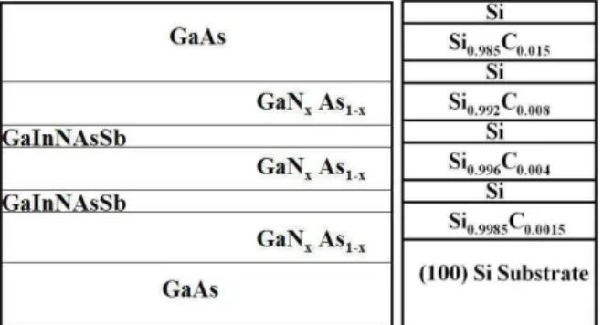
A schematic diagram of two types of sample used in this study is shown in Fig. 1. The dilute nitride sample consists of a double-quantum well (DQW) laser diode structure containing three 20 nm thick GaNxAs1-x (x = 0.045 and 0.029) barrier layers and two 7 nm thick GaInNAsSb quantum
wells. The dilute Si1-yCy sample consists of four Si1-yCy individual strained layers of 30 – 60 nm
thickness of increasing nominal composition (y = 0.0015, 0.004, 0.008 and 0.015 from bottom to top) separated by 50 nm thick Si spacers. These samples were grown by MBE [1,2,8]. A 200 kV JEOL JEM-2100F TEM/STEM equipped with a ADF detector, a DigiScan, a Gatan Imaging Filter (GIF) Tridiem and an Oxford INCA energy dispersive X-ray spectrometer (EDX) was used for this study. The thickness of the various TEM cross-section samples was determined from the ratio of the plasmon to the zero-loss peaks in the electron energy loss spectrum. Care has been given to
precisely adjust “gain” and “brightness” of the ADF detector in order to obtain accurate and meaningful intensity measurements [9].
Figure 1. Schematic diagram of samples (a) GaNxAs1-x and (b) Si1-yCy RESULTS AND DISCUSSION
A. GaNxAs 1-x/GaAs sample
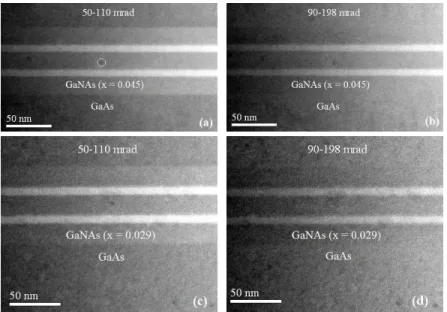
Figure 2 displays four ADF-STEM images acquired at 50 and 90 mrad ADF detector inner semiangles. Two of them are from the GaN0.045As0.955 sample (Fig. 2a and 2b), and the other two are
from the GaN0.029As0.971 sample (Fig. 2c and 2d). It is observed that there is a large intensity
difference between the GaNxAs1-x and GaAs layers at lower detector inner semiangles (Fig. 2a and
2c). The sample thicknesses are 37 nm and 41 nm, respectively. Contradictory to the compositional contrast prediction of ADF-STEM image intensity, the lower average atomic number GaNxAs1-x
layers (atomic numbers are 31.415 and 31.623 for GaN0.045As0.955 and GaN0.029As0.971, respectively)
were brighter than the surrounding higher average atomic number GaAs (atomic number is 32 for GaAs) for the ADF detector inner semiangles of 50 mrad (Fig. 2a and 2c). At the higher inner
Figure 2. ADF-STEM images acquired at two different detector semiangles for GaN0.045As0.955
sample (a and b) and GaN0.029As0.971 sample (c and d).
detector semiangle of 90 mrad, normal ADF-STEM image Z contrast is obtained: the intensity of GaNxAs1-x is slightly lower than that of GaAs (Fig. 2b and 2d).
Since the ADF-STEM image composition contrast cannot explain the above observations, we need to take the strain into consideration. In the hetero-epitaxial growth of GaNxAs1-x layers on a
GaAs substrate, there are two types of strains in the GaNxAs1-x layers. One is the lattice mismatch
strain due to the difference in lattice constant between GaNxAs1-x layers on GaAs substrates. The
other is the atomic size mismatch strain arising from the atomic radius difference between the substitutional N (rN = 0.068 nm) and As host (rAs = 0.121 nm) atoms. It has been shown by
multislice simulations that the atomic size mismatch strain plays a crucial role in the observed ADF-STEM image contrast, while the contribution to the contrast due to lattice mismatch strain between GaNxAs1-x and GaAs is small [10]. The agreement between the experimental and multislice
calculations for GaNxAs1-x (x = 0.045 and 0.029) sample is shown in Fig. 3.
20 30 40 50 60 70 80 90 100 0.00 0.05 0.10 0.15 0.20 x = 0.045 Experimental x = 0.029 Experimantal
x = 0.045 Multislice/atomic mismatch strain x = 0.029 Multislice/atomic mismatch strain
Detector inner semi-angle (mrad)
C o n tr a st ( IGa N A s /IG a A s -1 )
Figure 3. The experimental contrast between GaNxAs1-x and GaAs compared to multislice
B. Si1-yCy /Si sample
In the Si1-yCy/Si sample, the atomic number of SiC (atomic number is 13.88 for Si0.985C0.015)
is slightly lower than that of Si (14), and the atomic radius of C (rC = 0.068 nm) is much smaller
than that of Si (rSi = 0.120 nm). Since there is a significant atomic size mismatch strain between
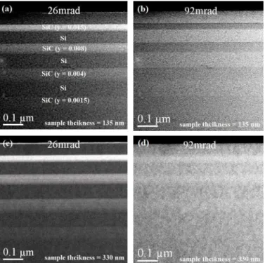
substitutional C and host Si atoms, the reversed ADF-STEM image contrast between SiC layer and Si substrate is expected as compared to the GaNxAs1-x/GaAs system. Figure 4 shows ADF-STEM
images acquired at two different inner detector semiangles of 26 and 92 mrad and at two different sample thicknesses of 135 nm and 330 nm. For a 26 mrad detector inner semiangle, the lower atomic number SiC layer is brighter than higher atomic number Si for both 135 nm and 330 nm samples (Fig. 4a and 4c). At 92 mrad detector inner semiangle, normal ADF-STEM Z contrast was obtained for the 135 nm thick sample (Fig. 4b), while reversed ADF-STEM image contrast
remained for the 330 nm thick sample (Fig. 4d). Thus, this atomic size mismatch induced reversed ADF-STEM image contrast between dilute semiconductor epitaxial layers and substrate depends on the sample thickness. At relatively thick sample, SiC always scatters more electrons than that of Si for scattering angles up to 92 mrad [11].
Figure 4. ADF-STEM images acquired at two different detector semiangles for Si1-yCy sample with
sample thickness 135 nm (a and b) and 330 nm (c and d).
APPLICATIONS
ADF-STEM imaging combined with EDX and EELS allow the simultaneous
characterization of crystal morphology, structure, and composition in a STEM. However both EDX and EELS failed to determine C composition in the Si1-yCy sample because the C concentration was
beyond the detection limit of both EDS and EELS. It is noted that a strong contrast between Si and Si1-yCy layers was observed in certain ADF-STEM images (Fig. 4). This contrast can be correlated
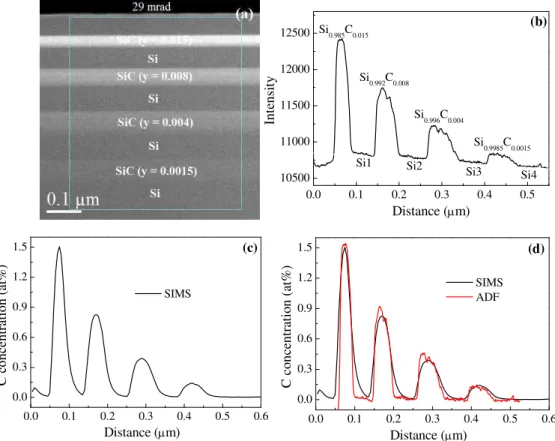
profile and the C composition profile of the Si1-yCy as obtained by secondary ion mass spectrometry
(SIMS) are compared. Figure 5a is an ADF-STEM image acquired at 29 mrad detector semiangle and 330nm sample thickness. The intensity line profile was integrated over a width of 0.48 m (Fig. 5b). By adjusting the Si0.985C0.015 layer ADF-STEM image intensity to a 1.5 at% C peak
concentration, the C composition profiles as determined by SIMS (Fig. 5c) coincides remarkably well with the ADF-STEM image line intensity profile for all four Si1-yCy layers (Fig. 5d). In fact,
details of the STEM-ADF C concentration profile in Fig. 5 may be linked to experimental
conditions prevailing during the MBE deposition of the Si/Si1-yCy staircase structure. For example,
the slow increase in C content from the bottom to top in the more dilute layers may be correlated with transients and stabilization periods of the ECR plasma C source. Instabilities in the ECR source may also have caused local C composition variations that are revealed by spikes in the ADF-STEM profile, but that could not be resolved by SIMS. Also, ADF-STEM exhibits a better depth resolution than SIMS and reveals that the Si/Si1-yCy interfaces chemically sharper than what SIMS would
suggest. Finally, it is interesting to note that the integrated ADF-STEM intensity from the upper Si 1-yCy layers is somewhat lower than that observed in SIMS. This may be correlated to the fact that
some C atoms are known to occupy non-substitutional sites in epitaxial Si1-yCy layers with C
composition in excess of 0.01 [2]. This may indicate that here the non-substitutional C fraction do not contribute significantly to the ADF-STEM contrast.
Figure 5. (a) An ADF-STEM image acquired with 29 mrad ADF detector inner semiangle and
sample thickness of 330 nm. (b) The intensity line profile from image (a). (c) C composition profile obtained with SIMS. (d) Comparison of the C composition SIMS profile with ADF-STEM image intensity line profile.
0.0 0.1 0.2 0.3 0.4 0.5 10500 11000 11500 12000 12500 Si0.996C0.004 Si 0.9985C0.0015 Si0.992C0.008 Si4 Si0.985C0.015 Si3 Si2 In te n si ty Distance ( m) Si1 (b) 0.0 0.1 0.2 0.3 0.4 0.5 0.6 0.0 0.3 0.6 0.9 1.2 1.5 SIMS ADF C c o n ce n tr at io n ( at % ) Distance ( m) (d) 0.0 0.1 0.2 0.3 0.4 0.5 0.6 0.0 0.3 0.6 0.9 1.2 1.5 SIMS C c o n ce n tr at io n ( at % ) Distance ( m) (c)
CONCLUSIONS
The reversed ADF-STEM image contrast between dilute semiconductor heteroepitaxial strained layers and substrates was observed in GaNxAs1-x/GaAs and Si1-yCy/Si systems. The lower
average atomic number heteroepitaxial strained layers GaNxAs1-x and Si1-yCy are brighter than the
higher average atomic number GaAs and Si substrates for ADF detector semiangle up to 92 mrad. The localized strain due to the atomic size mismatch between the substitutional atoms (N, C) and host atoms (GaAs, Si) is responsible for the reversed ADF-STEM image contrast. The intensity line profile of the ADF-STEM images showed excellent agreement with composition profiles obtained by SIMS for Si1-yCy/Si sample. In conjunction with another analytical technique such as SIMS or
x-ray diffraction, the ADF-STEM image line intensity profile of dilute Si1-yCy/Si system may thus
provide a means to estimate C concentration variation in the Si1-yCy/Si system at concentrations
beyond the detection limit of either EDX-STEM or EELS-STEM and spatial resolution exceeding that of SIMS.
REFERENCES
1. J.A. Gupta, P.J. Barrios, J.A. Caballero, D. Poitras, G.C. Aers, G. Pakulski and X. Wu, Appl. Phys. Lett. 89 (2006) 151119.
2. J.-M. Baribeau et al, Thin Solid Films, 410 (2002) 61.
3. X. Wu, J.-M. Baribeau, J.A. Gupta and M. Beaulieu, J. Crystal Growth, 282 (2005) 18. 4. X. Wu and G. C. Weatherly, Phil. Mag. A., 81 (2001) 1489.
5. D.B. Williams and C.B. Carter, Transmission Electron Microscopy, (Plenum Press, New York, 1996), p.360.
6. D.E. Jesson, S.J. Pennycook and J.-M. Baribeau, Phys. Rev. Lett. 66 (1991) 750. 7. P. Hartel, Ultramicroscopy, 63 (1996) 93.
8. J.A. Gupta, I.S. Sproule, X. Wu and Z.R. Wasilewski, J. Crystal Growth 291 (2006) 86. 9. X. Wu et al., Mater. Res. Soc. Symp. Proc. 982E (2007) KK01-03.
10. X. Wu, M.D. Robertson, J.A. Gupta and J.-M. Baribeau, J. Phys: Condens. Matter, 20 (2008) 075215.