HAL Id: hal-00449480
https://hal.archives-ouvertes.fr/hal-00449480
Submitted on 21 Jan 2010
HAL is a multi-disciplinary open access
archive for the deposit and dissemination of
sci-entific research documents, whether they are
pub-lished or not. The documents may come from
teaching and research institutions in France or
abroad, or from public or private research centers.
L’archive ouverte pluridisciplinaire HAL, est
destinée au dépôt et à la diffusion de documents
scientifiques de niveau recherche, publiés ou non,
émanant des établissements d’enseignement et de
recherche français ou étrangers, des laboratoires
publics ou privés.
A low-power high-gain LNA for the 60GHz band in a 65
nm CMOS technology
Michael Kraemer, Daniela Dragomirescu, Robert Plana
To cite this version:
Michael Kraemer, Daniela Dragomirescu, Robert Plana. A low-power high-gain LNA for the 60GHz
band in a 65 nm CMOS technology. Asia Pacific Microwave Conference 2009, Dec 2009, Singapore,
Singapore. �hal-00449480�
A low-power high-gain LNA for the 60 GHz band
in a 65 nm CMOS technology
Michael Kraemer
#∗1, Daniela Dragomirescu
#∗2, Robert Plana
#∗3 #CNRS ; LAAS ; 7 avenue du colonel Roche, F-31077 Toulouse, France∗University of Toulouse ; UPS, INSA, INP, ISAE ; LAAS ; F-31077 Toulouse, France
1
[email protected]; [email protected]; [email protected]
Abstract— One essential building block for integrated 60 GHz
CMOS radio transceivers is the low noise amplifier (LNA). This paper presents a two-stage cascode LNA fabricated in the 65 nm bulk CMOS technology of ST Microelectronics. It occupies 0.4 mm x 0.4 mm die area (pad-limited). For the matching networks, lumped elements are employed exclusively. It can be biased using two different supply voltages: When using 1.5 V, a peak gain of 22.4 dB and an output-referred 1 dB compression point of−3.4 dBm is measured while drawing 11.2 mA supply current. The simulated noise figure is 4.5 dB. When using a supply voltage of 1.0 V, a peak gain of 18.7 dB and an output-referred 1 dB compression point of -6.5 dBm is measured while drawing 8.5 mA supply current. The simulated noise figure is 5.2 dB.
I. INTRODUCTION
A major research topic in the domain of microwave engi-neering today is the design of low-cost transceiver front-ends for the unlicensed frequency band around 60 GHz. While the first CMOS circuits for this purpose were designed in a 130 nm technology [1], the use of lower scale CMOS technologies with higher unity gain frequencies (fT, fmax) is one way to
improve performance. However, the potential advantages are accompanied by drawbacks such as lower breakdown voltages (and thus decreased linearity), more stringent density rules and scaling of the metal back-end.
This paper deals with one of the basic building blocks of such a transceiver, the low noise amplifier (LNA), implemented in a 65 nm CMOS technology.
Employing the Friis equation [2] in the form NFtot = NFLNA+NF
2− 1
GLNA
(1) gives the overall noise figure (NF) of a receiver as a function of the NF of the LNA, the NF of the subsequent circuit elements (NF2) and the gain of the LNA. Note that a high LNA gain is
thus essential to achieve good receiver performance, because it allows to screen the usually much higher noise figures of the subsequent stages. Consequently, the two major requirements for the LNA are low noise figure and high gain.
Concerning linearity, the last block is the most important one, as an equation similar to (1) points out [2]. Because the subsequent mixer stage is usually limiting the linearity of the receiver, it is not sensible to maximize the LNA’s linearity at the expense of higher DC power consumption. Moreover,
strong inband interferers are not to be expected in the 60 GHz band, which loosens the requirements on the intermodulation points of the LNA.
In addition to the above mentioned requirements, very low power consumption and small chip area are very important for battery-driven, low cost applications.
II. DESIGN OF THELNA
The LNA presented in this paper employs two single-ended cascode stages as illustrated in Fig. 1. The cascode topology allows for good stability and excellent reverse-isolation, which is especially important in direct-conversion architectures. The algorithm of [3] is followed throughout design.
The first stage is optimized for very low noise. Therefore, the transistors are biased around minimum NF current density at 0.15mA/μm [4]. The widths of the transistors M1 and M3 are chosen to be22 × 1μm in order to yield a real part of the optimum noise impedanceRSOPTthat equals50 Ω to facilitate
matching. All transistors used in the design have a minimum drawn gate length of 60 nm.
The inductorLm1forms an artificial transmission line together
with the parasitics of M1 and M3, and thus increases thefT
of the cascode. The value of Lm1 is 87 pH. A degeneration
inductor is added at the source of M1 to allow a simultaneous
Lin Lm2 Lm1 LL1 VDD M1 M3 M4 M2 Cc IN OUT Cout LL2 VDD Ldeg Cin D1 TL D2 VDD VDD
Fig. 1. Simplified schematic of the designed two-stage cascode LNA (parasitic diodesD1andD2due to deep n-wells surrounding M3 and M4)
noise and power match of the LNA input. Using Ldeg =
97 pH, the real part of the input impedance yields around 50 Ω, without changingRSOPT.
The input of M1 has to be matched to the 50 Ω source impedance in parallel with the 25 fF pad capacitance. Because the imaginary part of the optimum noise impedance XSOPT
is roughly equal to the negative imaginary part of the input of M1, a simultaneous noise and conjugate match is achieved. The matching network consisting of Cin =55 fF, a 50 Ω
transmission line of length 25 μm, and Lin = 139 pH is
designed using the Smith chart for a match around 60 GHz. The second stage is optimized for high gain. Therefore, the transistors are biased at the maximumfTcurrent density [5]
around 0.3 mA/μm. The transistors M2 and M4 have a width of26 × 1μm and thus are slightly larger than M1 and M3 for improved linearity of this second stage. The middle inductor for the second stage was chosen to beLm2 = 73 pH.
The input and output of the second stage are power matched to the preceding stage and the load impedance (50 Ω in parallel to the pad capacitance). The values for the input matching network areLL1=125 pH and CC=210 fF, the values for the
output matching network areLL2=139 pH and Cout =38 fF.
The maximum allowable supply voltage used for the cas-code stages depends on the transistors employed. Generally, a higher VDD yields higher performance at the expense of
increased power consumption. While the presented circuit was designed for a VDD of 1.5 V, a lower supply voltage (an
example throughout this paper is 1 V) can be employed to reduce power consumption.
A. Transistors
The employed 65 nm technology provides low power (LP) and general purpose (GP) transistors. The LP transistors offer higher gate oxide thickness and thus reduced leakage currents and an increased breakdown voltage (1.2 V instead of 1.0 V). While in digital designs leakage is directly linked to the static power consumption, in millimeter-wave circuits the transistors are biased at high current densities, compared to which the leakage currents are negligible.
Furthermore, as shown in [5], the LP transistors exhibit anfT
way below the one of GP transistors (e.g. 135 GHz in lieu of 180 GHz for 65 nm CMOS as presented in [5]). This shows that for a transistor biased at a given power consumption, GP devices exhibit superior performance, mandating their use for low power circuit design.
One consequence of the use of GP transistors is the lower breakdown voltage of 1 V. A remedy used during LNA design is to embed the cascode transistors into a deep n-well: In doing so, they are isolated from the grounded substrate and drain and gate voltages in excess of 1 V become feasible.
To simulate the behavior of the GP transistors, a BSIM4 model is employed. While the intrinsic performance is well represented by this model, the custom layout is not taken into account. However, the extrinsic performance of the transistors is highly layout-dependent [6]. To obtain an extrinsic model that takes into account the optimized multi-finger layout used,
first, the gate resistance is calculated according to equation (1) of [3]. Secondly, a parasitic extraction is performed. The extrinsic model obtained this way is used during all phases of the LNA design.
B. Passive Devices
The passives used during LNA design include capacitors and inductors employed for matching and decoupling. The capacitors used are metal-on-metal (MOM) finger capacitors, because MIM capacitors have too low a quality factor at millimeterwaves.
As inductive matching elements, spiral inductors are used rather than distributed elements. This is possible even at 60 GHz because their size remains small compared to the wavelength for the used values. Moreover, their performance with respect to size, realizable values and quality factor are superior to transmission lines when using CMOS technologies with low resistivity substrates [7], [8].
The design of the spiral inductors is done similar to the ap-proach lined out in [8]. However, the focus lies on minimizing the parasitics rather than maximizing the quality factor, which would limit the LNA’s bandwidth.
This minimization of parasitics is done by using only the thick top-most metal layers and minimizing both conductor width and total spiral area over substrate. Electromagnetic simulations using HFSS, Sonnet and ASITIC are employed to do quantitative optimizations. Simulations done using these three programs agree very well with each other. The S-parameters obtained by simulation of the final geometry are used to parametrize a (2)-π model, which is employed in linear and non-linear simulations to predict circuit behavior. The issue of strong coupling between adjacent inductors is addressed by surrounding them by a grounded metal structure consisting of several metal layers. By this means, the path of the ground return current is also clearly defined and can thus be taken into account during electromagnetic simulations.
C. Fabricated Circuit
Following the circuit design outlined above, the layout of the circuit is done. Besides the accurately modeled inductors and the small piece of transmission line at the input of the circuit interconnect lengths were short enough to be neglected. The presented circuit was fabricated in the 65 nm CMOS technology of STMicroelectronics with two thick copper metal layers. Fig. 2 shows a photo of the fabricated circuit. Four bias pads and 2 GSG pads for the 60 GHz in- and output surround the LNA core.
III. RESULTS
Measurements up to 65 GHz are performed using an Anritsu ME7808A vector network analyzer. A SOLT calibration moves the reference planes to the probe tips. No de-embedding of the pads is required as their capacitance is taken into account by the circuit’s matching network.
The measurement of the circuit performance is done at two dif-ferent bias points: The first high gain bias point atVDD=1.5 V
Fig. 2. Photo of the fabricated LNA, circuit dimensions 400μm x 400 μm including pads.
requires a supply current of 11.2 mA and thus yields a power consumption of 16.8 mW. The second low power bias point employsVDD=1.0 V, drawing 8.5 mA supply current and thus
exhibiting a power consumption of 8.5 mW.
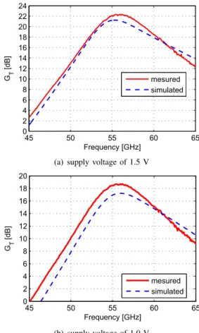
The transducer power gainGT at these bias points is shown
in Fig. 3(a) and 3(b), respectively. Peak gain values of 22.4 dB and 18.7 dB, both at 56 GHz, are achieved, showing good agreement with simulation results.
The input and output matching of the LNA at the high gain bias point is illustrated in Fig. 4 (for the low power bias point the curves are very similar). A Return loss (RL) inferior to -20 dB is measured around 56 GHz. Furthermore, on the basis of the S-parameter measurements, unconditional stability of the LNA is verified.
In order to quantify the linearity of the LNA, its output power (Pout) is measured versus the input power (Pin) thus obtaining
the -1 dB compression point(P−1dB). In Fig. 5 this curve is plotted together with the uncalibrated gain at the high gain bias point. AP−1dB of -3.4 dBm is measured, which is sufficient according to the system considerations of section I. For the low
power bias point,P−1dB equals -6.5 dBm (curve not shown). The presented results stem from one single die. Measurements of several other dies of the same wafer confirm the obtained results very closely.
The NF of the LNA has not yet been measured due to lack of measurement capabilities at 60 GHz. The NF simulation results are shown in Fig. 6 for both bias points. Measurement results are expected to be very close due to the use of BSIM4 models and the fact that all parasitics are taken into account during simulation.
IV. COMPARISON TO THESTATE OF THEART
Table I presents a performance overview comparing 60 GHz CMOS LNAs found in literature to the work presented in this paper. General observations are that the noise figure decreases with scaling of technology, and that circuits using lumped elements exhibit smaller size and better over-all per-formance. The LNA presented in this paper yields low power
45 50 55 60 65 0 2 4 6 8 10 12 14 16 18 20 22 24 Frequency [GHz] GT [dB] mesured simulated
(a) supply voltage of 1.5 V
45 50 55 60 65 0 2 4 6 8 10 12 14 16 18 20 Frequency [GHz] G T [dB] mesured simulated (b) supply voltage of 1.0 V
Fig. 3. Small signal transducer power gainGTof the LNA, measurement results versus Cadence SPECTRE simulation
consumption and the best compromise for all LNAs using a cascode topology, showing the interest of using a 65 nm CMOS technology for LNA design. The work presented in [7] shows the interest of using small transistor widths and a more simple common source topology, if the high reverse isolation of a cascode is not necessary.
V. CONCLUSION
The high-gain low-power LNA presented in this paper exhibits state-of-the-art performance, yielding the ideal com-promise for the input stage of a low-cost low-power 60 GHz receiver. First pass design success was achieved by extracting transistor parasitics and using electromagnetic simulations to model the employed inductors.
Key points in circuit design are the use of inductors, the embedding of the cascode transistor in a deep n-well to allow higher supply voltages, and the use of a 65 nm CMOS technology for low power-consumption and low noise. To minimize coupling effects, a differential version of this LNA should be implemented if power consumption is less of an issue.
ACKNOWLEDGEMENT
Thanks go to Prof. Sorin Voinigescu of University of Toronto and his students for valuable hints on mm-wave circuit design and Alexandre Rumeau for measurement support.
TABLE I
PERFORMANCE COMPARISON TOLNAS FOUND IN LITERATURE
Ref. Techn. Freq. max.GT P−1dB min. NF VDD Power Area Topology Matching [nm] [GHz] [dB] [dBm] [dB] [V] [mW] [mm2]
[1] 130 60 12 +2 8.8 1.5 54 1.3× 1 3-stage cascode distributed [9] 130 56 24.7 +1.8 7.1 2.4 79.2 0.72× 0.67 3-stage cascode distributed [10] 130 53 14 -6 6.1 1.2 10.6 0.91× 0.58 4-stage common source # distributed ##
[6] 90 60 12.2 +4 6* 1.0 10.4 1.27× 0.38 2-stage common source distributed [3] 90 58 14.6 -0.5 5.5 1.5 24 0.4× 0.35 2-stage cascode lumped [11] 90 60 16 +1 6 1.8 29 N.A. 2-stage cascode distributed [12] 90 64 15.5 +3.8 5.2 1.65 85.8 1.3× 0.4 2-stage cascode distributed [12] 90 64 13.5 N.A. N.A. 1.26 47.9 1.3× 0.4 2-stage cascode distributed
[7] 90 58 15 -4 4.4 1.3 3.9 0.32× 0.44 3-stage common source lumped [13] 65 60 11.5 1.5 5.6 1.2 72 0.87× 0.7 3-stage common source distributed [14] 65** 64 12 -5 8 2.2 36 0.96× 1.05 2-stage cascode distributed this work 65 56 22.4 -3.4 4.5* 1.5 16.8 0.4× 0.4 2-stage cascode lumped this work 65 56 18.7 -6.5 5.2* 1.0 8.5 0.4× 0.4 2-stage cascode lumped
*simulated; **SOI; # current reuse; ## also one inductor used
35 40 45 50 55 60 65 −60 −50 −40 −30 −20 −10 0 Frequency [GHz] RL [dB] |S 11| [dB] |S 22| [dB]
Fig. 4. Return loss (RL) measured at the input and output of the LNA biased atVDD=1.5 V.
REFERENCES
[1] C. Doan, S. Emami et al., “Millimeter-wave CMOS design,” IEEE
Journal of Solid State Circuits, vol. 40, no. 1, pp. 144–155, Jan. 2005.
[2] B. Razavi, RF microelectronics. Upper Saddle River, NJ, USA: Prentice-Hall, Inc., 1998.
[3] T. Yao, M. Gordon et al., “Algorithmic design of CMOS LNAs and PAs for 60-GHz radio,” IEEE Journal of Solid State Circuits, vol. 42, no. 5, pp. 1044–1057, May 2007.
[4] S. Voinigescu, T. Dickson et al., “A comparison of Si CMOS, SiGe BiCMOS, and InP HBT technologies for high-speed and millimeter-wave ICs,” in IEEE SiRF, Sept. 2004, pp. 111–114.
[5] S. Nicolson, E. Laskin et al., “Design and modeling considerations for fully-integrated silicon w-band transceivers,” in IEEE RFIT, Dec. 2007, pp. 141–149.
[6] B. Heydari, M. Bohsali et al., “Low-power mm-wave components up to 104 GHz in 90nm CMOS,” in IEEE ISSCC, 11-15 Feb. 2007, pp. 200–597.
[7] E. Cohen, S. Ravid, and D. Ritter, “An ultra low power LNA with 15dB gain and 4.4dB NF in 90nm CMOS process for 60 GHz phase array radio,” IEEE RFIC, pp. 61–64, April 17 2008.
[8] T. Dickson, M.-A. LaCroix et al., “30-100-GHz inductors and transform-ers for millimeter-wave (Bi)CMOS integrated circuits,” IEEE Trans. on
MTT, vol. 53, no. 1, pp. 123–133, Jan. 2005.
[9] C.-M. Lo, C.-S. Lin, and H. Wang, “A miniature V-band 3-stage cascode LNA in0.13μm CMOS,” IEEE ISSCC, pp. 1254–1263, Feb. 2006. [10] H.-Y. Yang, Y.-S. Lin et al., “A low-power V-band CMOS low-noise
amplifier using current-sharing technique,” in IEEE ISCAS, May 2008, pp. 964–967. −32 −30 −28 −26 −24 −22 −20 −18 18 19 20 21 22 23 P in [dBm] GT [dB] −32 −30 −28 −26 −24 −22 −20 −18 −10 −7.5 −5 −2.5 0 2.5 Pout [dBm] Gain Pout P−1dB
Fig. 5. Plot of measured transducer power gainGTand output powerPout versus input powerPinto obtain the -1dB compression point.
45 50 55 60 65 4 5 6 7 8 9 10 Frequency [GHz] NF [dB] V DD=1.0V V DD=1.5V
Fig. 6. Simulated noise figure for supply voltages of 1V and 1.5V.
[11] S. Pinel, S. Sarkar et al., “A 90nm CMOS 60 GHz radio,” in IEEE
ISSCC, 3-7 Feb. 2008, pp. 130–601.
[12] S. Pellerano, Y. Palaskas, and K. Soumyanath, “A 64 GHz LNA with 15.5 dB gain and 6.5 dB NF in 90 nm CMOS,” IEEE Journal of Solid
State Circuits, vol. 43, no. 7, pp. 1542–1552, July 2008.
[13] M. Varonen, M. Karkkainen, and K. Halonen, “Millimeter-wave ampli-fiers in 65-nm CMOS,” in 33rd ESSCIRC, Sept. 2007, pp. 280–283. [14] A. Siligaris, C. Mounet et al., “CMOS SOI technology for WPAN.