HAL Id: hal-03184764
https://hal.archives-ouvertes.fr/hal-03184764
Submitted on 29 Mar 2021
HAL is a multi-disciplinary open access
archive for the deposit and dissemination of
sci-entific research documents, whether they are
pub-L’archive ouverte pluridisciplinaire HAL, est
destinée au dépôt et à la diffusion de documents
scientifiques de niveau recherche, publiés ou non,
Thermal performance of GaInSb quantum well lasers for
silicon photonics applications
C. R. Fitch, G. W. Read, I. P. Marko, D. A. Duffy, L Cerutti, J-B Rodriguez,
E Tournié, S. J. Sweeney
To cite this version:
C. R. Fitch, G. W. Read, I. P. Marko, D. A. Duffy, L Cerutti, et al.. Thermal performance of GaInSb
quantum well lasers for silicon photonics applications. Applied Physics Letters, American Institute of
Physics, 2021, 118 (10), pp.101105. �10.1063/5.0042667�. �hal-03184764�
Thermal performance of GaInSb quantum well
lasers for silicon photonics applications
C. R. Fitch,1 G. W. Read,1 I. P. Marko,1 D. A. Duffy,1 L. Cerutti,2 J-B. Rodriguez, 2 E. Tournié,2
and S. J. Sweeney1, a)
AFFILIATIONS
1Advanced Technology Institute and Department of Physics, University of Surrey, Guildford GU2 7HX, United Kingdom
2IES, Université de Montpellier, CNRS, F-34000 Montpellier, France
a)Author to whom correspondence should be addressed: s.sweeney@surrey.ac.uk
ABSTRACT
A key component for the realization of silicon-photonics are integrated lasers operating in the important communications band near 1.55 µm. One approach is through the use of GaSb-based alloys which may be grown directly on silicon. In this study, silicon-compatible strained Ga0.8In0.2Sb/Al0.68 In0.32Sb composite quantum well (CQW) lasers grown on GaSb substrates emitting at 1.55 μm have been developed and investigated in terms of their thermal performance. Variable temperature and high-pressure techniques were used to investigate the influence of device design on performance. These measurements show that the temperature dependence of the devices is dominated by carrier leakage from the QW region to the Xb minima of the Al0.35Ga0.65As0.03Sb0.97 barrier layers accounting for up to 43% of the threshold current at room temperature. Improvement in device performance may be possible through refinements in the CQW design, while carrier confinement may be improved by optimization of the barrier layer composition. This investigation provides valuable design insights for the monolithic integration of GaSb-based lasers on silicon.
The realization of optoelectronic integrated circuits (OEICs) requires an efficient, silicon-compatible electrically pumped laser operating above room temperature (RT). The indirect nature of silicon makes it unsuitable as an active region. While heterogeneous integration may currently be the most advanced approach in terms of device performance1, the longer term goal is direct epitaxial growth of III-V lasers on silicon1. However, the lattice constant and thermal expansion coefficient mismatch and the polar/ non-polar interface between silicon and traditional III-V laser materials causes large defect densities, leading to inefficient and unreliable lasers. Progress has been made in overcoming these challenges through the use of GaAs based 1.3 μm quantum dot lasers on silicon2,3 and Ga(NAsP)/GaP/Si quantum well (QW) lasers at 800-900 nm4. However, an alternative material system and approach is required for long-haul telecoms applications operating around 1.5 μm.
Sb-containing alloys are of interest for growth on silicon since dislocations tend to propagate parallel to the Si/III-V-Sb interface rather than into the active layers, allowing growth of high-quality active regions. GaInSb/GaSb composite quantum well (CQW) lasers have been grown by molecular beam epitaxy on 4°-off (001) silicon substrates emitting at 1.55 µm at RT in pulsed mode5; near 1.55 µm in continuous wave (c.w.) on GaSb near RT6; and more recently at 1.59 µm c.w. at RT on 6° miscut silicon7. However, further development is needed to address high threshold current densities (Jth) and temperature sensitivity8.
To commercialize on-silicon devices, it is important to understand the efficiency limiting mechanisms of the equivalent active regions grown on GaSb. In this paper we report on the thermal properties of GaInSb CQW devices on GaSb substrates6 and use a range of experimental techniques to identify the principal processes limiting device performance16.
2 The test devices (A, B, C) illustrated in figure 1, consist of three compressively strained Ga0.8In0.2Sb QWs. The Al0.35Ga0.65As0.03Sb0.97 barriers and Al0.9Ga0.1As0.07Sb0.93 cladding layers are lattice-matched to the GaSb substrate.
Material Thickness (nm) p-GaSb(100) 300 Graded p-AlGaAsSb 100 pAl0.9Ga0.1As0.07Sb0.93 1000 Al0.35Ga0.65As0.03Sb0.97 200 Ga0.8In0.2Sb 3.6 (A), 4.8 (B), 6 (C) Al0.35Ga0.65As0.03Sb0.97 20 Ga0.8In0.2Sb 3.6 (A), 4.8 (B), 6 (C) Al0.35Ga0.65As0.03Sb0.97 20 Ga0.8In0.2Sb 3.6 (A), 4.8 (B), 6 (C) Al0.35Ga0.65As0.03Sb0.97 200 nAl0.9Ga0.1As0.07Sb0.93 1000 Graded n-AlGaAsSb 100 n-GaSb(100) substrate
FIG. 1. Test device structures.
Devices B and C are CQWs formed by the insertion of one (B) and two (C) 0.45 nm Al0.68In0.32Sb barriers within each Ga0.8In0.2Sb QW. The insertion of AlInSb monolayers into the wider wells introduces additional confinement, counteracting the reduction in bandgap caused by the additional width. Further details of the fabrication of these devices is given in reference6.
Pulsed electrical injection (500 ns, 10 kHz) was used to minimize current heating effects. Device characteristics were measured as a function of temperature from 40-300 K using a closed-cycle cryostat system. Figure 2(a) shows the facet output intensity (L) variation with current density (J) and temperature (T) for representative device B. Figure 2(b) shows the extracted Jth variation with temperature for all three devices.
For these lattice-matched devices, defect-related recombination is assumed to be negligible in the QW region and at low temperatures, where Jth is low, other forms of non-radiative recombination are also assumed negligible. For an ideal QW laser at low temperatures the radiative component of threshold current density, Jrad ∝ T 9 and for our devices Jrad can be seen to dominate threshold below ~150 K.
FIG. 2. (a) Temperature dependent LI (device B);
(b) threshold current densities and radiative components (all devices).
The Jrad components at RT were approximated by linear extrapolation of the low temperature Jth to 300 K shown as the shaded area in figure 2(b) and in Table I.
TABLE I. Threshold current densities and radiative
components at 300 K.
Device A Device B Device C
Jth (Acm-2) 1092 654 471
Jrad (Acm-2) 170±6 147±10 189±5
Jrad/Jth (%) 15±1 23±2 40±1 For T > 150 K, Jth increases super-linearly, suggesting the onset of non-radiative processes such as Auger recombination or carrier leakage consistent with evidence from other laser types at this wavelength10.
In a simple model Jth can be expressed as16: 𝐽𝑡ℎ= 𝑒𝐿𝑧(𝐴𝑛 + 𝐵𝑛2+ 𝐶𝑛3) + 𝐽𝑙𝑒𝑎𝑘 (1) Where e is the electronic charge, Lz is the active layer thickness, n is the carrier density (assuming equal electron and hole carrier densities) and A, B and C are the recombination coefficients for defect, radiative and Auger recombination respectively. The Jleak term accounts for carrier leakage from the QWs.
0 100 200 300 400 500 600 0 10 20 30 40 50 60 Int en sity (a .u .)
Current density (Acm-2) 60 K 140 K 100 K 180 K 220 K 260 K 300 K (a) 0 50 100 150 200 250 300 0 200 400 600 800 1000 1200 Th resh old c urrent den sity (Ac m -2) Temperature (K) Device A Device B Device C 1092 Acm-2 654 Acm-2 Jrad (b) 471 Acm-2
Auger recombination and carrier leakage are strongly temperature dependent which may explain the strong increase in Jth with temperature11. The reduction in J
th at RT from device structures A to B to C may be attributed to the increased gain volume, which reduces the threshold carrier density, nth, by lowering the band filling and increasing the photon generation rate for a given injection current. Increased optical confinement would also contribute to the reduction in nth by increasing modal gain and the stimulated emission rate.
Approaching room temperature Jth increases exponentially and, over a limited temperature range, this increase may be described by the characteristic temperature T012: 𝑇0= (𝑑𝑙𝑛(𝐽𝑑𝑇 )𝑡ℎ) −1 = (𝐽1 𝑡ℎ 𝑑𝐽𝑡ℎ 𝑑𝑇 ) −1 (2)
A higher T0 is desirable as it corresponds to greater thermal stability of Jth. Expressions for the characteristic temperature due to radiative, Auger recombination and leakage effects can be derived as12: 𝑇0(𝐼𝑟𝑎𝑑) = 1 + 2𝑥𝑇 (3) 𝑇0(𝐼𝐴𝑢𝑔) = 𝑇 3 + (𝐸𝑎 𝑘𝑇) + 3𝑥 (4) 𝑇0(𝐼𝑙𝑒𝑎𝑘) = 𝑇 (𝐸𝑎 𝑘𝑇) (5)
Where x is a “non-ideality” factor, e.g. due to optical losses, and Ea is the respective activation energy for the Auger or leakage process.
The theoretical variation of T0(T) for Jth can be written as a weighted average of the individual T0 values: 1 𝑇0= 1 𝑇0(𝑟𝑎𝑑)𝑅 + 1 𝑇0(𝑛𝑜𝑛𝑟𝑎𝑑)(1 − 𝑅) (6)
where R(T) is defined as Jrad/Jth and T0(nonrad) corresponds to either the Auger or leakage process. T0(T) was measured using a five-point average and compared with a numerical model to investigate the non-radiative contribution to
Jth.
FIG. 3. Experimental and modelled characteristic temperature and threshold current density (a) T0 (radiative and leakage) (b) T0 (radiative and Auger) (c) Jth (radiative and leakage) (d) Jth (radiative and Auger).
0 50 100 150 200 250 300 0 20 40 60 80 100 120 140 160 180 200 T0 (K) Temperature (K) Device A measured T0 Device B measured T0 Device C measured T0 Fitted To(rad+leak)
T0leak=T/(Ea(leak)/kT) TB Devices A and B T0rad=T/(1+2x) TB Device C (a) 0 50 100 150 200 250 300 0 20 40 60 80 100 120 140 160 180 200 T0 (K) Temperature (K) Device A measured T0 Device B measured T0 Device C measured T0 Fitted To(rad+Aug)
T0Aug=T/(Ea(Aug)/kT) TB Devices A and B T0rad=T/(1+2x) TB Device C (b) 0 50 100 150 200 250 300 0 100 200 300 400 500 600 700 Device B measured Jth Fitted Jth(rad+leak) Fitted Jrad Fitted Jleak Device B J th (Acm -2) Temperature (K) JradT Jleak=J0exp(-Ea(leak)/kT) (c) 0 50 100 150 200 250 300 0 100 200 300 400 500 600 700 Device B measured Jth Fitted Jth(rad+Auger) Fitted Jrad Fitted JAuger Device B J th (Acm -2) Temperature (K)
JAug=J0exp(-Ea(Aug)/kT)
JradT
(d)
4 Figure 3(a) shows the measured and modelled T0(T) for all three devices for radiative recombination and carrier leakage together with the radiative and leakage limits for device B as an example. Figure 3(b) shows that a similarly good fit may be achieved assuming radiative and Auger recombination. At low temperatures T0 tends towards the radiative limits while above a break-point temperature, TB16, it tends towards the leakage or Auger limits. The difference in
T0(T) between the three structures is consistent with the trends in Jth and highlights the improvement in performance with increasing composite well thickness where a lower nth leads to a reduction in non-radiative recombination. Figures 3(c) and 3(d) show the example of the measured Jth for device B and the result of fitting the radiative and leakage (a) or radiative and Auger (b) components from the T0 model. A similar quality of fit is found for devices A and C. The T0 data may therefore be explained by considering either leakage or Auger recombination although it is not possible to distinguish which is dominant from this analysis alone.
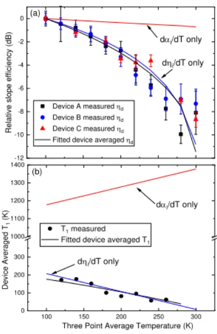
Using a similar approach we investigated the temperature sensitivity of the differential quantum efficiency (slope) above threshold, ηd where:
𝜂𝑑∝𝑑𝐿𝑑𝐼 (7)
The characteristic temperature T1 is defined as ηd(T)=η0exp(-T/T1) where η0 is a constant13, so: 𝑇1= − (𝑑ln (𝜂𝑑𝑇 )𝑑) −1 = − (𝜂1 𝑑 𝑑𝜂𝑑 𝑑𝑇 ) −1 (8)
Equation (8) was applied using a three-point average to plot the experimental values of T1.
The differential quantum efficiency ηd may be expressed as:
𝜂𝑑= 𝜂𝑖𝛼 𝛼𝑚 𝑖+ 𝛼𝑚
(9) Here ηi is the internal quantum efficiency, αi is the internal loss and αm the mirror loss expressed as: 𝛼𝑚= 𝐿1 𝑐𝑎𝑣𝑙𝑛 1 𝑅𝑓 (10)
where Lcav is the cavity length and Rf the as-cleaved facet reflectivity. Assuming the change
in αm with temperature is negligible we deduce that: 𝑇1= 1 1 (𝛼𝑖+ 𝛼𝑚) 𝑑𝛼𝑖 𝑑𝑇 −𝜂1𝑖 𝑑𝜂𝑖 𝑑𝑇 (11)
Terms on the left-hand side of the denominator relate to cavity losses and on the right-hand side to injection losses (e.g. carrier leakage). This decomposition allows investigation of the relative contributions to T1. We used a least squares numerical fit model to vary dαi/dT and dηi/dT to fit to the measured
ηd(T) using equation (11).
Figure 4(a) shows the relative change in slope efficiency ηd for all three device structures. Figure 4(b) shows the measured and modelled average T1 values. The limits associated with varying only αi or ηi with temperature are also shown.
FIG. 4. Experimental and modelled slope efficiency
(a) and characteristic temperature T1 (b). From this fit it is clear that dηi/dT dominates with dαi/dT having negligible effect. This confirms that the temperature sensitivity of T1 is due to injection rather than optical losses and supports the T0 analysis which identified carrier leakage as a possible contributory factor. It also indicates that Inter Valence Band Absorption
-12 -10 -8 -6 -4 -2 0 Relative slop e e fficien cy (d B) Device A measured hd Device B measured hd Device C measured hd
Fitted device averaged hd
dhi/dT only dai/dT only (a) 100 150 200 250 300 0 100 200 300 1000 1100 1200 1300 1400 Device Aver ag ed T1 (K)
Three Point Average Temperature (K) T1 measured
Fitted device averaged T1 dai/dT only
dhi/dT only (b)
(IVBA) and Free Carrier Absorption (FCA) are not significant because they are associated with the αi rather than the ηi contribution to ηd. Auger recombination is not expected to influence the T1 analysis since n is (ideally) pinned above threshold. An important outcome of the T1 analysis is that the efficiency data can only be explained by the presence of carrier leakage.
Both carrier leakage and Auger recombination are sensitive to band structure. Hydrostatic pressure can be used to reversibly change the band structure of a semiconductor, hence it was used to assess the dependence of the device performance on the band structure. Pressures up to 400 MPa were applied using a Unipress helium compressor system, details of which may be found in11.
The measured variation of Jth with pressure is shown in figure 5(a).
FIG. 5. (a) Threshold current density variation with
pressure - Experimental measurements (solid symbols) and theoretical dependence of the individual current paths and best fit with pressure (device B) (b) schematic band alignment.
A numerical model was created to describe how Auger recombination and carrier leakage vary with pressure to investigate their quality of fit to the experimental data.
In an ideal QW laser, where optical losses are negligible, Jrad scales with bandgap according to Jrad∝ Eg2.
The pressure dependence of the leakage and Auger components take the form:
𝐽𝑛𝑜𝑛𝑟𝑎𝑑= 𝐽0𝑒𝑥𝑝 [− (𝑑𝐸𝑑𝑃 )𝑎 𝑘𝑃 𝑏𝑇]
(12)
Where J0 = 1 for normalized data and dEa/dP is the net change in the respective activation energy with pressure.
For leakage, dEa/dP corresponds to the net change in band alignment between the quasi-Fermi level in the conduction band, taken to be equal to the QW electron ground state (e1), and the energy of the states into which the carriers escape. We assume that e1 changes as dElase/dP and the valence band alignment is approximately pressure independent14. dE
lase/dP
was measured to be ~11 meVkbar-1 for all three devices.
CHSH Auger recombination (where the energy of a Conduction band electron recombining with a hole in the Heavy hole band is given to a third hole in the Heavy hole band which is excited into the Spin split-off band) is sensitive to the difference between the band gap (Eg) and the spin-orbit (SO) split-off-energy (ΔSO). For our devices where Eg>ΔSO, the CHSH activation energy is given by:
𝐸𝑎(𝐶𝐻𝑆𝐻) =2𝑚 𝑚𝑠𝑜
ℎ+ 𝑚𝑐− 𝑚𝑠𝑜(𝐸𝑔− ∆𝑆0) (13) where mc and mh are the electron and heavy hole band, in-plane, effective masses and mso is the SO split-off band effective mass.
The CHCC Auger activation energy is: 𝐸𝑎(𝐶𝐻𝐶𝐶) =𝑚𝑚𝑐
𝑐+ 𝑚ℎ𝐸𝑔
(14) CHCC refers to electron-hole recombination between the Conduction and Heavy hole bands accompanied by excitation of a Conduction band electron further into the Conduction band. In (13) and (14) Eg changes according to
dElase/dP. From k.p theory, mc and mso increase approximately proportionally to band gap, and hence pressure, while mh is relatively independent of pressure15. QW effective masses were calculated from a linear interpolation of the binary components from Vurgaftman et al16.
6 Other Auger processes have been ignored since they have previously been shown to be relatively weak10,17. Due to the closeness of the e
1 and ΔSO energies, CHSH is expected to dominate the Auger current at wavelengths < 2 μm18.
An increasing Jth with pressure is generally a strong indicator of carrier leakage from the QW to the indirect X or L valleys. In contrast,
Jth decreases with pressure for CHSH/CHCC Auger processes, or for leakage from the QW to the barrier Γbband edge (when the barrier Γb band edge pressure coefficient is smaller than the QW, as here).
The QW e1 to barrier Γb, Xb and Lb minima energy offsets were calculated at RT and ambient pressure for the three structures by combining the binary energy gaps, bowing parameters and valence band offsets from Vurgaftman et al16, accounting for strain in the QW.
For the three structures, the range of values are: e1-Γb = 218-223 meV; e1-Xb = 275-280 meV; and e1-Lb = 299-304 meV (e1-cladding separations were all >439 meV), figure 5(b). While these energy offsets should be sufficient to confine the majority of carriers, the Fermi-Dirac distribution of carriers extends into these energies where there is a high density of states, hence increasing the recombination rate. It was also found that the energy offsets and configuration of the barrier minima are very sensitive to the bowing parameters which vary considerably in the literature16, 19.
As evident from figure 5(a), the increase in
Jth with pressure is stronger than that expected for leakage to the Lb-valley states. However, it is consistent with leakage to the Xb-valley dominating the increase in Jth. A good fit to the experimental results was achieved for all devices using a combination of radiative recombination, leakage to the barrier Xb minima (forming up to 43% of Jth), and a contribution of CHSH/CHCC Auger recombination or leakage to the barrier Γb or Lb minima. Shockley-Read-Hall (SRH) is likely to be a strong factor in the subsequent recombination of carriers in the barrier material.
The results of this study demonstrate the potential of GaSb-based QW lasers for silicon photonics applications in the telecoms wavelength range and opportunities for ongoing improvement.
We showed that the strong temperature sensitivity of Jth could be explained by either
leakage or Auger recombination. However, the temperature sensitivity of ηd was found to be dominated by carrier injection, confirming that leakage must be present. Furthermore, from pressure-dependent measurements, carrier leakage from the QW active region to the barrier Xb valley states was found to be a key limiting factor in the performance of these devices. This could be reduced by increasing the activation energy of the leakage paths by a small increase in the lattice matched barrier Al and As fractions and without compromising optical confinement provided by the cladding. Further improvement in reducing Jth and thermal sensitivity might also be achieved by increasing the number of QWs although the relatively small improvements associated with increased gain volume of device C over B compared with B over A suggests diminishing scope for improvement. Optimization would also benefit from a detailed investigation of bowing parameters and band alignments in this system.
Acknowledgments This work has been partly supported by EPSRC (UK) under grant EP/N021037/1, a SEPnet PhD scholarship for D. A. Duffy, the French ANR (Project OPTOSi, No. ANR-12-BS03-002) and by the French “Investment for the Future” program (EquipEx
EXTRA, No. ANR-11-EQPX-0016).
Data Availability The data associated with this work are available by request at https://doi.org/10.5281/zenodo.4353309.
REFERENCES
1
C. Cornet, Y. Leger, and C. Robert, Integrated
Lasers on Silicon (ISTE Press, 2016). 2 M. Liao, S. Chen, S. Chen, S. Huo, J. Wu, M. Tang, K. Kennedy, W. Li, S. Kumar, M. Martin, T. Baron, C. Jin, I. Ross, A. Seeds, and H. Liu, IEEE J. Sel. Top. Quantum Electron. 23, (2017).
3 D. Jung, Z. Zhang, J. Norman, R. Herrick, M.J. Kennedy, P. Patel, K. Turnlund, C. Jan, Y. Wan, A.C. Gossard, and J.E. Bowers, ACS Photonics 5, 1094 (2018).
4
S. Liebich, M. Zimprich, P. Ludewig, A. Beyer, K. Volz, W. Stolz, B. Kunert, N. Hossain, S.R. Jin, and S.J. Sweeney, Proc. 22nd IEEE Int. Semicond. Laser Conf. 143 (2010).
5 L. Cerutti, J.B. Rodriguez, and E. Tournie, IEEE Photonics Technol. Lett. 22, 553 (2010). 6 L. Cerutti, A. Castellano, J.B. Rodriguez, M.
Bahri, L. Largeau, A. Balocchi, K. Madiomanana, F. Lelarge, G. Patriarche, and E. Tournié, Appl. Phys. Lett. (2015).
7 A. Castellano, L. Cerutti, J.B. Rodriguez, G. Narcy, A. Garreau, F. Lelarge, and E. Tournié, APL Photonics 2, 061301 (2017).
8 E. Tournié, A. Castellano, K. Madiomanana, G. Narcy, A. Garreau, F. Lelarge, J.-B. Rodriguez, and L. Cerutti, Mol. Beam Ep. 625 (2018).
9
P. Blood, Quantum Confined Laser Devices, First (Oxford University Press, 2015).
10 S.R. Jin, S.J. Sweeney, S. Tomić, A.R. Adams, and H. Riechert, IEEE J. Sel. Top. Quantum Electron. 9, 1196 (2003).
11 A.F. Phillips, S.J. Sweeney, A.R. Adams, and P.J.A. Thijs, IEEE J. Selcted Top. Quantum Electron. 5, 401 (1999).
12 E.P. O’Reilly and M. Silver, Appl. Phys. Lett. 63, 3318 (1993).
13 N. Tansu, Y.L. Chang, T. Takeuchi, D.P. Bour, S.W. Corzine, M.R.T. Tan, and L.J. Mawst, IEEE J. Quantum Electron. 38, 640 (2002).
14 W. Mönch, Electronic Properties of
Semiconductor Interfaces (Springer Series in Surface Sciences book series (SSSUR, volume 43), 2004).
15 A. Krier, X.L. Huang, and V. V Sherstnev,
Mid-Infrared Semiconductor Optoelectronics (Springer Series in Optical Sciences book series (SSOS, volume 118), 2006).
16 I. Vurgaftman, J.R. Meyer, and L.R. Ram-Mohan, J. Appl. Phys. 89, 5815 (2001).
17 A. Sugimura, IEEE J. Quantum Electron. 19, 930 (1983).
18 S.J. Sweeney, G. Knowles, T.E. Sale, and A.R. Adams, Phys. Status Solidi Basic Res. 223, 567 (2001).
19
S. Adachi, Properties of Semiconductor Alloys:
Group-IV, III-V and II-VI Semiconductors (Wiley Series in Materials for Electronic & Optoelectronic Applications, 2009).