HAL Id: hal-02526080
https://hal.archives-ouvertes.fr/hal-02526080
Submitted on 3 Jul 2020HAL is a multi-disciplinary open access archive for the deposit and dissemination of sci-entific research documents, whether they are pub-lished or not. The documents may come from teaching and research institutions in France or abroad, or from public or private research centers.
L’archive ouverte pluridisciplinaire HAL, est destinée au dépôt et à la diffusion de documents scientifiques de niveau recherche, publiés ou non, émanant des établissements d’enseignement et de recherche français ou étrangers, des laboratoires publics ou privés.
Reconfigurable 2D/0D p-n Graphene/HgTe Nanocrystal
Heterostructure for Infrared Detection
Ulrich Nguétchuissi Noumbé, Charlie Gréboval, Clément Livache, Audrey
Chu, Hicham Majjad, Luis Parra López, Louis Donald Notemgnou Mouafo,
Bernard Doudin, Stéphane Berciaud, Julien Chaste, et al.
To cite this version:
Ulrich Nguétchuissi Noumbé, Charlie Gréboval, Clément Livache, Audrey Chu, Hicham Majjad, et al.. Reconfigurable 2D/0D p-n Graphene/HgTe Nanocrystal Heterostructure for Infrared Detection. ACS Nano, American Chemical Society, 2020, �10.1021/acsnano.0c00103�. �hal-02526080�
Reconfigurable 2D/0D p-n Graphene/HgTe Nanocrystal Heterostructure for Infrared Detection
Ulrich Nguétchuissi Noumbé1&, Charlie Gréboval2&, Clément Livache2, Audrey Chu2, Hicham
Majjad1, Luis E. Parra López1, Louis Donald Notemgnou Mouafo1, Bernard Doudin1, Stéphane
Berciaud1,3, Julien Chaste4, Abdelkarim Ouerghi4, Emmanuel Lhuillier2*, Jean-Francois Dayen1,3* 1Université de Strasbourg, CNRS, Institut de Physique et Chimie des Matériaux de Strasbourg
(IPCMS), UMR 7504, 23 rue du Loess, Strasbourg, 67034, France.
2Sorbonne Université, CNRS, Institut des NanoSciences de Paris, INSP, F-75005 Paris, France 3 Institut Universitaire de France, 1 rue Descartes, 75231 Paris cedex 05
4 Centre de Nanosciences et de Nanotechnologies, CNRS, Université Paris-Saclay, C2N,
Palaiseau 2110, France.
Abstract: Nanocrystals are promising building blocks for the development of low-cost infrared
optoelectronics. Gating a nanocrystal film in a phototransistor geometry is commonly proposed as a strategy to tune the signal to noise ratio by carefully controlling the carrier density within the semiconductor. However, the performance improvement has so far been quite marginal. With metallic electrodes, the gate dependence of the photocurrent follows the gate-induced change of the dark current. Graphene presents key advantages: (i) infrared transparency that allows back-side illumination, (ii) vertical electric field transparency and (iii) carrier selectivity under gate bias. Here, we investigate a configuration of 2D/0D infrared photodetectors taking advantage of a high capacitance ionic glass gate, large scale graphene electrodes, and a HgTe nanocrystal layer of high carrier mobility. The introduction of graphene electrodes combined with ionic glass enables to reconfigure selectively the HgTe nanocrystals and the graphene electrodes between electrons (n) and holes (p) doped states. We unveil that this functionality enables to design a 2D/0D p-n junction that expands throughout the device, with a built-in electric field that assists charge dissociation. We demonstrate that in this specific configuration, the signal to noise ratio for infrared photodetection can be enhanced by two orders of magnitude, and that photovoltaic operation can be achieved. The detectivity now reaches 109 Jones while the device only absorbs 8% of the incident light.
Additionally, the time response of the device is fast (<10 µs) which strongly contrasts with the slow response commonly observed for 2D/0D mixed dimensionalities heterostructures, where larger photoconduction gains come at the cost of slower response.
Keywords: HgTe, narrow band gap nanocrystals, infrared detection, gate induced diode, graphene.
& these two authors have equal contributions
*To whom correspondence should be sent: lhuillier@insp.upmc.fr, dayen@unistra.fr
Among possible applications for colloidal nanocrystals (NCs), low cost short-wave and mid-wave infrared photodetectors are raising more and more interests.1,2 HgTe appears as the most tunable
material to address these ranges of wavelength, thanks to the semimetal nature of the bulk material.3,4 Significant progresses over the recent years have transformed the concept from an
infrared (IR) absorbing material to high performance detectors with near unity absorption5,6 or dual
color detection.7,8 With progress in mastering the fabrication and understanding of this material,
HgTe has also been used as a platform for IR integrated photonics,9,10 gas sensing11 or electronics.12
There are nevertheless many issues that still need to be addressed. Among them there are (i) the need for IR transparent electrodes and (ii) the energy band profile of HgTe-based devices which is not yet optimized for charge dissociation. In this paper, we propose a structure which addresses these two current limitations.
In the visible and near infrared ranges, oxides such as tin doped indium oxide are commonly used as transparent conductive electrodes. Such doped oxides present a plasmonic absorption13,14 in the
infrared that limits their use as transparent electrodes. To overcome this issue, it has been proposed to reduce the thickness of the oxide6,15 but this comes at the price of a higher contact resistance.
Alternatively, very thin layer of metal16 or a metal grid array17 have been used as charge collector.
Again, there is a clear trade-off between absorption and contact resistance in these cases too. In the short and mid-wave infrared (λ<5 µm), the absorption of graphene is extremely limited (2%) and quickly after its discovery, graphene has appeared as a good candidate for electrode design.18–22 The coupling of NCs with 2D materials has been mostly investigated in the so-called mixed dimensional Van der Waals heterostructure geometry,23 revealing properties and functionalities that
already lead to prospects for quantum electronics,24 spintronics25,26 and optoelectronics.27,28
For photodetection applications, the driving idea was to take advantage of both the high carrier mobility29 of 2D materials and the strong tunable light absorption of NCs. Graphene devices
functionalized with PbS NCs have thus led to exceptionally high responsivities27,30 (>106 A/W), and
this concept was then extended to longer wavelengths using HgTe NCs.31 To date, most of these
pioneer works engineer their device architecture such that charge transport occurs only into the graphene conducting channel, while nanocrystals are simply used as light sensitizer that injects carriers into graphene. Hence, while this approach allows for large responsivity, it comes at the price of some key limitations such as the large dark current in the structure, and dramatically slow time response.32 To reduce the dark current, it was later proposed to replace the gap-less graphene by
MoS2.33 Nevertheless, the device concept remains similar and some limitations persist, as in these
mixed dimensional heterostructures the coupling between the 2D material and NCs occurs through a tunnel process and only the NCs in the very vicinity of the 2D material are actually contributing to the photoconduction.
Here, we propose a change of paradigm compared to previous 2D/0D photodetectors : we show that for 2D/0D devices, charge transport should involve the nanocrystal film to absorb more strongly the incident light. This requires to make the conduction within the nanocrystal array more efficient using a ligand exchange step to get high carrier mobility.
In this manuscript, we report about a way to induce p-n junction directly into the nanocrystal thin film by combining three key elements: (i) the unique electronic properties of graphene electrodes,(ii) the recent developments of HgTe NCs-based inks15 leading to films with relatively high carrier mobility34
(>1 cm2v-1s-1), and (iii) the use of high capacitance ionic glass gating technology 35–37 that enables
to reach high carrier density and to spatially tune the doping profile through the whole 2D/0D heterostructure. Our study demonstrates that the built-in electric field of the p-n junction formed into the nanocrystal film allows for enhancing the charge dissociation and unlock photovoltaic functionality.
Devices based on vertical geometry have certainly led to the highest detection performance reported so far. However, the choice of the layers involved in the device currently obeys empirical laws and offers no post-processing tunability. In this sense, the planar transistor geometry offers more flexibility through gating. Gating of HgTe thin films has been obtained with a variety of gates from conventional dielectrics,11,34,38 to electrolytes39,40 and more recently using ionic glasses.37 In the
conventional operation mode of a transistor, the drain source bias is low compared to the gate bias. This limits the charge dissociation compared to what is achieved in vertical geometry devices. In addition, even if the gate allows a certain tunability of the responsivity, the increase of the photocurrent is greatly balanced by the rise of the dark current.11,37,41 There is however another
operating mode for transistor, which is the diode mode. In this case, a large drain-source bias is used, inducing opposite carrier density (ie electron vs hole) for the drain and source electrodes. This mode has been extensively used to design gate-induced light emitting diodes,42–45 in particular in organic compounds.46–48 In this paper, we demonstrate that graphene-based electrodes combined with ionic glass gating offer an interesting platform for the design of gate-induced 2D/0D p-n junction. Graphene combines three key advantages compared to metallic electrodes: (i) infrared transparency which allows back-side illumination of the device. (ii) Graphene being a semimetal with a low density of state compared to metal, it is possible to tune the Fermi level below and above the Dirac point. This makes the design of carrier-selective electrodes (ie electron or hole extractor) possible. Last, (iii) graphene is thinner than its Thomas-Fermi screening length and thus partially transparent to the vertical electric field induced by the underneath gate. Consequently, the p and n parts of the gate-induced junction have a much larger spatial extension into the NC thin film compared to what is achieved with metallic electrodes. Such gate-induced 2D/0D p-n junction can be used to enhance the charge dissociation directly inside the HgTe nanocrystals array and boost the device photocurrent. We bring clear evidence that the behavior of the graphene-HgTe-graphene junction strongly differs from its equivalent based on gold contacts, and allow the design of reconfigurable heterojunctions, fast and improved photoresponse, and photovoltaic operation.
Results and discussion
We start by designing a graphene-HgTe NC-graphene junction. To do so, we have grown HgTe NCs using the procedure provided by Keuleyan et al. 49 The obtained nanocrystals have a multipodic
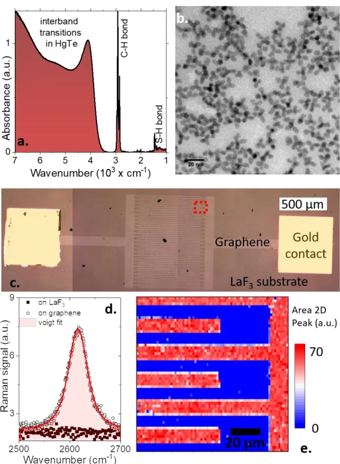
shape with a typical size around 8 nm, see Figure 1b. The particles present an interband-edge at 4000 cm-1 (≈0.5 eV or 2.5 µm), according to their infrared spectrum, see Figure 1a. Previous
investigation of the electronic structure of the material has revealed that the work function of the pristine material is equal to 4.6±0.1 eV, while the Fermi level is located in the upper part of the band gap (Vb-EF=0.3 eV).50
The devices are constructed over a LaF3 substrate, which is an infrared transparent ionic glass
(allowing back side illumination of the sample). This ionic glass is also used as a back-side gate dielectric. Under application of a potential difference over the two sides of the substrate, the F- ions
migrate in the bulk matrix, allowing the LaF3 substrate to present a larger gate capacitance than
conventional or even high-k dielectrics.35,51 The freezing temperature of the ions (below 180 K)
remains much lower than the one of ion gel electrolyte, making it suitable for IR photodetection as recently demonstrated on HgTe NCs arrays37 and atomically thin transition metal dichalcogenides
layers.35,51
On the top of this LaF3 substrate, chemical vapor deposition (CVD) monolayer graphene is
transferred and processed using laser lithography methods to create interdigitated electrodes (see
Figure 1c) made of a total of 50 digits, 750 µm long, 10 µm wide and spaced by 10 µm from its
neighbors. The Raman 2D peak is used as an unambiguous fingerprint of the presence of graphene and allows mapping of the interdigitated pattern, see Figure 1d and e. The full width at half maximum of the 2D Raman peak is found to be 46 cm-1 (Figure 1d), a value somewhat larger than in
mechanically exfoliated monolayers suggesting52 a contribution from nanoscale strain variations53
consistent with the targeted pattern (Figure 1e), confirming that graphene is fully etched between the digits.
Figure 1 Material under consideration. a. Absorption spectrum of HgTe NCs. b. Transmission electron microscopy image of HgTe NCs. c. Microscopy image of the graphene interdigitated electrodes on a LaF3 substrate. The area in the red square is mapped using Raman spectroscopy
(laser wavelength = 633 nm) in part e. d. Raman spectra of the graphene electrode on LaF3. e. Map
of the intensity of the Raman 2D peak (2616 cm-1) in the area of the graphene interdigitated
To form a conductive array of HgTe NCs, we use a phase transfer method which aims at preparing a NC (photo)conductive ink. At the end of the procedure, HgTe nanoparticles are capped with short ligands (mercaptoethanol and HgCl2 in this case15). Before building the HgTe-graphene junction, it
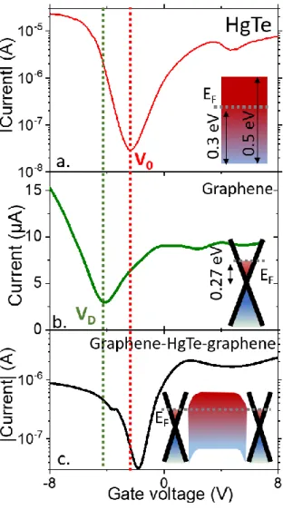
is of utmost interest to reveal the transport properties of each material independently over the same LaF3 gate to account for possible charge transfer between the material and the substrate. Metallic
gold electrodes are used to build an HgTe device that presents a clear ambipolar behavior with a charge neutrality point (V0) appearing under negative gate bias at –2.3 V, see Figure 2a. We can
anticipate a n-doping of the material in absence of gate, which is consistent with previous photoemission measurements.50 In the case of graphene deposited on LaF3, we build a Hall bar
device used in four-probe configuration to measure the graphene intrinsic conductivity (Figure S1). The transfer curve of the bare graphene also reveals an ambipolar behavior with minimum of conductance at the Dirac point reached for a negative gate bias of 𝑉𝐷=𝑉𝐺𝑆 = −4.2 𝑉 , see Figure
2b. This suggests a partial electron transfer from the LaF3 to the graphene which displaces the Fermi
level above the Dirac point of graphene. From the gate bias associated to the Dirac point we can determine the relative position of the Fermi level with respect to the Dirac point thanks to the relation54 𝐸
𝐹 = ħ𝑣𝐹√ 𝜋𝐶𝐿𝑎𝐹3
𝑒 (𝑉𝐺− 𝑉𝐷) = 0.27 𝑒𝑉 with ħ the reduced Planck’s constant, 𝑣𝐹 the Fermi
velocity55 equals to 8x10⁵ m.s-1, 𝐶
𝐿𝑎𝐹3 the capacitance of the LaF3 substrate37 (0.4 µF.cm-2) and e
the elementary charge.
Interestingly, the transfer curve of the graphene-HgTe-graphene heterojunctions (see Figure 2c) demonstrates a preserved ambipolar behavior with a charge neutrality point at 𝑉𝐺𝑆=-1.8 V ≈ V0. This
value is very close to that of HgTe film contacted by gold electrode, see Figure 2a. The deposited film of HgTe NCs is typically 120 nm thick, see Figure S2. The switching of graphene electrode doping state is reflected in the transconductance curve by an inflection of the transfer curve at the Dirac point VGS=-3.6 V ≈VD. From these transconductance measurements, we can describe the
band alignment in the graphene-HgTe-graphene junction: the Fermi level lies above the Dirac point and in the upper part of the semiconductor nanocrystals, see Figure 2c. In such junction, the key difference with metallic contact comes from the gate-tunable nature of the graphene doping level. The gate will not only tune the position of the Fermi level within the HgTe film but also within the electrodes. This enables the formation of electron and hole extracting layers.
Figure 2 Transport properties of HgTe NCs array and graphene. a. Transfer curve (drain current as a function of gate bias) for a HgTe NCs array on a LaF3 substrate and connected with gold electrode,
at 220 K. The inset is a scheme of the pristine HgTe electronic structure b. Transfer curve for a graphene Hall bar on a LaF3 substrate, at 240 K. The inset is a scheme of the pristine graphene
electronic structure. Both materials appear to be n-doped in absence of gate. c. Transfer curve for a HgTe NCs array on a LaF3 substrate and connected with graphene electrode, at 220 K. Scheme
of the electronic structure of graphene/HgTe/graphene junction assuming that the Dirac point is located at 4.6 eV from the vacuum level54 and that Fermi level is 0.27 eV above.
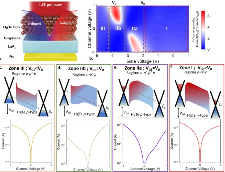
To better reveal the specificity of this 2D/0D heterostructure, we investigate in detail the graphene-HgTe-graphene current-voltage (I-V) characteristics dependence on ionic glass gate voltage VGS
(Figure 3, see also Figure S3). A schematic of the device is given in Figure 3a. We report, on
Figure 3b, the charge transport phase diagram of the 2D/0D device. It emphasizes on the evolution
of the asymmetry of the source-drain I-V curve (ratio of current at +VDS bias over current under -VDS
bias) under the back-gate voltage 𝑉𝐺𝑆.
Three different zones corresponding to distinct doping states of the graphene/HgTe heterojunctions can be discriminated: (i) For gate bias 𝑉𝐺𝑆 > 𝑉0 (zone I), exceeding the HgTe film charge neutrality point V0, we observe a symmetric quasi-ohmic I-V behavior, see Figure 3f. Under such condition
the Fermi level remains above the Dirac point for both electrodes, while the HgTe NCs film remains in the electron doping state, forming n-n’ junctions at the graphene/HgTe NC interfaces. (ii) When the gate bias is in the range 𝑉0 > 𝑉𝐺𝑆 > 𝑉𝐷 (zone II), the I-V curve acquires a rectifying behavior, see examples on Figure 3d and e. On Figure 3b., the high value of the current asymmetry (clearly
above 1) highlights the areas of occurrence (red part) of p-n junctions, with two distinct heterojunction configurations that can be discriminated. Details on the origin of these two distinct
p-n jup-nctiop-n regimes will be discussed below. Fip-nally (iii), up-nder large hole ip-njectiop-n, whep-n 𝑉𝐷 > 𝑉𝐺𝑆
(zone III), the two graphene electrodes and the HgTe film become hole-rich, and the I-V curve recovers its quasi-ohmic behavior, reflecting the formation of p-p’ junction, see Figure 3c.
We now discuss the ionic glass assisted doping mechanisms that enable the formation of the 2D/0D
p-n junctions in the zones IIa and IIb. First, it is worth pointing that, because of the large capacitance
of LaF3 substrate, applying moderate drain-source bias may lead to distinct vertical gate bias
conditions near the source and the drain electrodes. For gate bias voltage close to charge neutrality points of HgTe or graphene, this induce electron and hole doping in the vicinity of each electrode.
Figure 3 Evidence for gate induced p-n junction in the graphene/HgTe/graphene junction. a. Scheme of the field effect transistor under consideration where the gate is made of a LaF3 ionic substrate,
the drain and source electrodes are made of interdigitated graphene electrodes and the channel is made of HgTe NCs array. b. 2D color map of the asymmetry of the I-V curve, quantized through the ratio of the current under a given bias and the current under the opposite bias, as a function of the channel voltage between the source and drain electrodes, and gate voltage VGS. The regions in red
correspond to the existing domains for a p-n junction within the graphene/HgTe/graphene junction. c. Band alignment of the graphene/HgTe/graphene junction in the p-p’-p configuration and the associated quasi-ohmic I-V curve, in the zone III corresponding to the orange square in the phase diagram of part b. d. Band alignment of the graphene/HgTe/graphene junction in the n-p’-p configuration and the associated rectifying I-V curve, in the zone IIb corresponding to the green square in the phase diagram of part b. e. Band alignment of the graphene/HgTe/graphene junction in the n-n’-p’-n configuration and the associated rectifying I-V curve, in the zone IIa corresponding
to the purple square in the phase diagram of part b. f. Band alignment of the graphene/HgTe/graphene junction in the n-n’-n configuration and the associated quasi-ohmic I-V curve, in the zone I corresponding to the red square in the phase diagram of part b. All data are acquired at 220 K.
A first p-n junction state appears when 𝑉𝐺𝑆 gets closer to 𝑉0 (zone II.a, see figure Figure 3e), this
corresponds to p-n junction formation between electron-doped graphene electrodes and hole-doped HgTe NCs array, forming two back-to-back p-n junctions. A strong current asymmetry appears while increasing VDS amplitude (with value of the asymmetry clearly above 1 in the red area of the graph),
highlighting the formation of a p-n junction expanding throughout the HgTe film. Indeed, in the case of ambipolar semiconducting HgTe NC array, for gate bias below but close to the charge neutrality point VGS < V0≈-2 V, applying a negative VDS voltage on the drain electrode results in switching back
the HgTe doping state from p to n doped state. This creates a p-n junction within the HgTe thin film, with a p doped state at the source side and n doped state at the drain side.
The second p-n junction state (zone IIb) is triggered once 𝑉𝐺𝑆 is decreased down to 𝑉𝐷. There, applying source drain bias voltage results in Fermi level positioning on different sides of the Dirac point for the drain and source graphene electrodes (see band diagram in Figure 3d). One electrode gets electron rich while the other is hole rich, resulting in n-p diode on the drain side.
Hence, the observation of the p-n junction is made possible by the combination of the high capacitance gate from the LaF3, the tunable charge carrier polarities of graphene and HgTe NC
array, and the low electric screening of graphene. Electric charge density Δq at the graphene/LaF3
interface of the source (resp. drain) electrode is defined as Δq =CTOTx VGS (resp. Δq =CTOT x VDS).
The total capacitance is defined as 1/Ctot=1/CLaF3+1/CQ. Here CLaF3 is the ionic glass effective
capacitance, which at low frequency has been quantified by impedance spectroscopy to lay in the range CLaF3 ≈ 0.4 µF.cm-2 at 220 K. The quantum capacitance CQ captures the band filling of
graphene that results from its low density of states, and can be approximated by CQ≈e2D(EF), with
e the electron charge and D(EF) the graphene density of states at the Fermi energy.56–58
Experimental studies estimated CQ within 3 to 10 µF.cm-2 depending on the graphene doping level.
Given these orders of magnitude for the capacitances, approximately 90% of the charge induced by the ionic substrate are present on the top of the graphene, while no charge will be present in the case of metal electrodes. This low screening propagates the spatial extension of the p-n junction above the electrodes. Graphene thus plays a dual role: not only it allows carrier selectivity which first enables the formation of the p-n junction, but it also favors the spatial extension of the junction, leading to a higher volume of the HgTe film exposed to the gate-induced electric field.
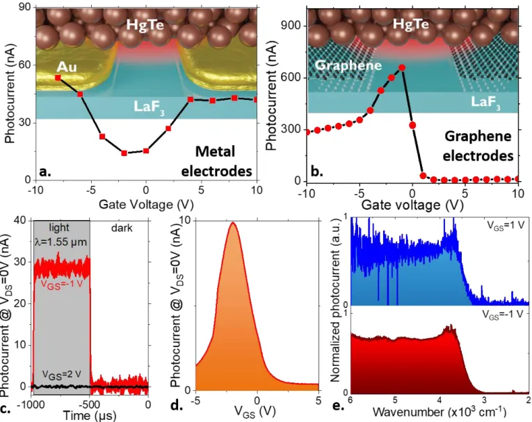
We have revealed in this device an interesting operating point where a 2D/0D p-n junction can be formed. In this case, a large electric field should appear at the interface between the hole and electron rich areas, which should enhance the charge dissociation. To confirm such predictions, we probe in Figure 4b the photocurrent in the graphene-HgTe-graphene junction illuminated by a short-wave infrared laser at 1.55 µm (i.e. above the band-edge of the HgTe nanocrystals). The curve presents a well-defined maximum of photocurrent in the range of gate bias corresponding to the existence of p-n junction formation (same as region II, introduced previously in Figure 3b.). This behavior dramatically differs from the one observed for the same HgTe film, with the same LaF3
gate but using gold metallic electrodes, see Figure 4a. In this case the responsivity is minimal at the minimum of conductance of HgTe. Conventional phototransistors actually display this kind of behavior, where photocurrent scales as the dark current. In other words, in usual (i.e. based on
metallic electrodes) phototransistors, applying gate bias enhances the photocurrent, but barely improves the signal-to-noise ratio. This behavior has been observed for many nanocrystals such as CdSe,59 or even HgTe with various dielectrics34 and electrolytic gates.41 Here with graphene
electrodes combined with high capacitance substrate, we can overcome this limitation. There is a gate bias window where photoresponse is maximized while the dark current is minimized, promoted by the formation of p-n junction through the 2D/0D heterostructure. Such regime is extremely promising for photodetection, as later discussed in the text.
Beyond the presence of an extremum in the responsivity magnitude as a function of gate bias, matching with the minimum of dark current, we can notice that the photoresponse is much higher under negative gate bias, ie under hole injection, compared to the value obtained under electron injection condition. This actually results from the initial n-type nature of the HgTe. By injecting holes in the material, it gets more intrinsic which reduces the recombination pathway for the minority carriers and thus extend their lifetime, leading to a larger photoconductive gain.
Figure 4 Photoresponse of the graphene/HgTe/graphene junction. a. Photocurrent as a function of gate bias for gold/HgTe/gold junction. The top part is a scheme of the device. b. Photocurrent as a function of gate bias for graphene/HgTe/ graphene junction. The top part is a scheme of the device. c. Photocurrent under 0 V drain source bias as the light (λ=1.55 µm) is turned on and off for two values of the gate bias. d. Photocurrent under 0 V, while the light is chopped at 1 kHz, as a function of the gate bias. e. Photocurrent spectra of the graphene/HgTe/graphene junction for two different gate bias. All data are acquired at 220 K.
The photovoltaic operation mode of the p-n junction, hallmark of the extension of the p-n junction into the NCs array, is further confirmed by the investigation of the photocurrent under zero applied electric field. Under positive gate bias, where no p-n junction exists, there is no photocurrent under zero drain-source bias, see Figure 4c and S5. Once the gate bias is applied within the window enabling the p-n junction formation, we observe a clear photo-signal even in absence of applied bias, which is the signature of built-in electric field. The magnitude of the photocurrent modulation at 1 kHz under zero drain source bias is given in Figure 4d and follows pretty well the data obtained under DC condition in Figure 4b. While the magnitude of the photocurrent spectrum also follows the same trend with gate bias, the shape of the spectral response remains unchanged for all gate bias, see Figure 4e and S4. In particular it is worth noticing that in spite of the large gate electric field associated with LaF3, no bleach of the band edge transition is observed.40 The p-n junction is formed
while the electron and hole carrier densities are kept well below 1 carrier per dot, which is critical to avoid any excessive increase of the dark current. More qualitatively, we can estimate the carrier density in the n and p area under 1V of drain source bias, assuming a balanced p-n junction. The sheet charge density induced by the gate is given by CLaF3*VDS/2e which corresponds to 1.25x10¹²
carrier.cm-2. If we assume the density is spread over the whole film thickness, this corresponds to a
volume density of 1x10¹⁷carriers.cm-3. We can estimate that the particle density is 2.4x10¹⁸
nanocrystals.cm-3, assuming a spherical shape for HgTe with a radius of 4 nm and a random close
packing (film density of 0.64). This means that the average gate induced doping density is 4x10⁻²
carrier per nanocrystal. This is far below 1 as expected from the photocurrent spectrum (i.e. no evidence for intraband absorption).
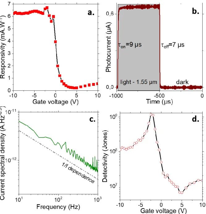
Figure 5 Infrared photodetection performance of the graphene/HgTe/graphene junction. a. Responsivity at 1.55 µm of the graphene/HgTe/ graphene junction, as a function of the applied gate bias. b. Temporal response of the graphene/HgTe/ graphene junction, under -1 V of gate bias. Dynamics appears to be limited by experimental setup. c. Current spectral density as a function of signal frequency, under -2.5 V of gate bias. The noise appears to be 1/f limited. d. Detectivity (ie signal to noise ratio) at 1 kHz and 220 K as a function of the applied gate bias for the graphene/HgTe/ graphene junction.
In the last section of the paper, we investigate the potential of this gate-induced p-n junction for infrared photodetection. Under moderate excitation power (ie irradiance of 133 µW.cm-2
corresponding to ≈1 µW of incident light on the sample) the responsivity reaches 6 mA/W under negative gate bias, see Figure 5a. The noise in the p-n junction appears to be 1/f limited, as commonly observed for NC array, 60,61 see Figure 5c. The detectivity clearly presents a maximum
1.2x10⁹ Jones for gate bias where the p-n junction is formed (see also Figure S8). This is typically
2 orders of magnitude larger than the value obtained for the same film in absence of p-n junction. This remains one order of magnitude weaker than the best value reported for HgTe based nanocrystals in vertical geometry.6,8 However, this limitation mostly results from the film thickness
above 500 nm and absorbing 30 % of the incident light and based on the same particles and surface chemistry achieved a detectivity of 3x10⁹ Jones.15 This indicates that charge dissociation is more
efficient in the planar p-n junction developed here than for current stack of nanocrystals used in HgTe nanocrystals based photodiode. Introduction of plasmonic resonators may be a viable way to solve this issue.5,6 The time response of the device has been found to be below 10 µs (Figure 5b),
with a weak incident power dependence (figure S6 and S7), which actually appears to be fully limited by the experimental setup. Note that the fast time response of our device is not driven by the large gate capacitance but rather by the capacitance of the nanocrystals film, which relates to HgTe thickness, its dielectric constant and the device area. Overall, our Graphene/HgTe nanocrystals heterostructures demonstrates a fast time response below a few µs which is enough for all video rate application. Such fast response strongly contrasts with the slower response commonly observed in quantum dots arrays coupled to 2D materials, usually locked in the tens of ms31 or even
slower.32 In such usual 2D/0D device geometry, absorption usually occurs in the quantum dot, and
the carrier with the lowest band offset with respect to the 2D material is transferred to the 2D layer, while the second carrier stays in the quantum dot. This photogating process leads to very large photoconduction gains and to large response but also hamper the current dynamics that gets driven by the recombination of the carrier trapped in the quantum dots array. In other words, the photogain increase is balanced by the drop of the device bandwidth. In our 2D/0D p-n junction geometry, the enhancement of the signal to noise ratio is obtained without degradation of the device bandwidth. In table S1, we have compared the performances of the device proposed here with the one reported in the literature based on infrared nanocrystal using various technology for the device (hybrid 0D-2D, photoconductor, phototransistor, and photodiode). Beyond the fast time response, our device offers an interesting tradeoff in term of signal to noise ratio and bandwidth, quantized in table S1 through the ratio of the detectivity over the time response. The device performance remains on the other hand, weaker than the best photodiode and this is mostly the result of the reduced absorption. The control of the light matter coupling5,6 is clearly a direction that need to be pushed for future work.
Conclusions
We have designed a phototransistor architecture based on a graphene-HgTe nanocrystals-graphene reconfigurable p-n junction. The formation of the p-n junction is made possible by the combination of the large gate capacitance of the infrared transparent LaF3 ionic glass, the carrier
selectivity of graphene and its partial transparency to vertical electric field. While previous phototransistors based on metallic electrodes were leading to marginal improvement of the signal to noise ratio under applied gate bias, the graphene electrodes/ionic glass combination enables a significant enhancement of the signal to noise ratio. The formation of a p-n junction, which widely expands over the nanocrystal film thickness thanks to the graphene low screening capability, allows to improve the device detectivity by more than two orders of magnitude under gate bias application, and to demonstrate extremely fast photoresponse time. The photovoltaic operation of the 2D/0D
p-n jup-nctiop-n is clearly exhibited by the presep-nce of photocurrep-nt up-nder zero draip-n source bias. Hep-nce,
while combining the high doping density provided by ionic glass, the electric field transparency and tunable charge carriers of graphene, and the large scale processability of nanocrystals, our 2D/0D device offers the possibility of being switched electrostatically from an IR phototransistor to a photovoltaic device. Finally, as p-n junction is the most ubiquitous component of modern electronics, the prospects opened by this 2D/0D p-n junction technology embrace a wider scope of application including integrated circuits, detectors, photovoltaics, and appears as highly promising approach to revisit the gate-induced light emitting diode.
Methods
Chemicals for nanocrystal synthesis: Mercury chloride (HgCl2, Strem Chemicals, 99%), Tellurium powder (Te, Sigma-Aldrich, 99.99%), trioctylphosphine (TOP, Cytek, 90%), oleic acid (Sigma, 90%), oleylamine (Acros, 80-90%), dodecanethiol (DDT, Sigma-Aldrich, 98%), chloroform (Carlo Erba), ethanol absolute anhydrous (Carlo Erba, 99.9%), methanol (Carlo Erba, 99.8%), toluene (Carlo Erba, 99.3%), All chemicals are used as received, except oleylamine which is centrifuged before used. Mercury compounds are highly toxic. Handle them with special care.
1 M TOP:Te precursor: 2.54 g of Te powder is mixed in 20 mL of TOP in a three neck flask. The
flask is kept under vacuum at room temperature for 5 min and then the temperature is raised to 100 °C. Furthermore, degassing of flask is conducted for the next 20 min. The atmosphere is switched to Ar and the temperature is raised to 275 °C. The solution is stirred until a clear orange coloration is obtained. The flask is cooled down to room temperature and the color switches to yellow. Finally, this solution is transferred to an Ar filled glove box for storage.
HgTe CQD synthesis with band edge at 4000 cm-1: 513 mg of HgCl2 was added to 60 mL of
oleylamine in a 100 mL round flask. The solution was placed under vacuum and heated to 110 °C for 1 h. Then, the temperature is decreased to 80 °C and solution placed under Ar atmosphere. 1.9 mL of TOP:Te (1 M) with 10 mL of oleylamine are added to the mercury solution. The solution color gradually turns to dark brown and the reaction is stopped 3 min. A solution made of 1 mL of dodecanethiol and 9 mL of toluene is quickly added to quench the reaction. The nanocrystals are then precipitated with ethanol. After centrifugation, the nanocrystals are redispersed in chloroform. The washing step is repeated one more time. The solution is filtered with a 0.2 µm filter and redispersed in 6 mL of chloroform.
Chemicals for ink preparation: n-hexane (VWR, 99%), N,N dimethylformamide (DMF, Sigma
Aldrich), 1,2 ethanedithiol (EDT, Fluka, 98%), mercaptoalcohol (MPOH, Merck, >99%).
HgTe CQD ink preparation: 5 mg of HgCl2, 100 µL of MPOH and 900 µL of DMF are mixed. 0.5 mL of this solution is added to 0.5 mL of a HgTe solution at 50 mg.mL-1 in toluene. A few mL of
hexane can be added to help phase dissociation: the QDs migrate to the bottom phase (DMF), showing efficient ligand exchange. After 3 washing steps with hexane, the QDs are mixed to 2-3 drops of ethanol and centrifuged at 6000 rpm for 2 min. The clear supernatant is discarded and the QDs are redispersed in 100 µL of fresh DMF to reach a concentration of 250 mg.mL-1. To ensure
the colloidal stability is good, the sample is then re-centrifuged at 3000 rpm for 4 min.
Material characterization: For TEM pictures, a drop of CQD solution is drop-casted on a copper
grid covered with an amorphous carbon film. The grid is degassed overnight under secondary vacuum. A JEOL 2010F is used at 200 kV for acquisition of pictures. For infrared spectroscopy we use a Fischer Nicolet iS50 in either Attenuated Total Reflection (ATR). The spectra are averaged over 32 acquisitions and have a 4 cm-1 resolution. Raman measurements were done with a
Labram-HR confocal microscope from Horiba, under ambient conditions. We used a 633 nm laser, with a power of 3 μW and a grating of 600 g / mm. The 2D peak of graphene fit with a single Lorentz peak. This results in a uniform graphene signal on the electrode.
Graphene electrode fabrication
Graphene interdigit contacts are formed by transferring a CVD-grown monolayer graphene onto LaF3 substrate (done by Grapheal62 following fabrication process detailed in reference63). Using
interdigits with 10 µm width and 750 µm length, spaced by 10 µm were patterned. The substrate is firstly cleaned with acetone and rinsed with ethanol and isopropanol. AZ 1505 resist is then spin-coated and baked at 105 °C. The well-defined area on the substrate is exposed under UV Laser. The exposed resist is developed using a bath of AZ 726 for 20 s, before being rinsed in DI water. We then used the mixture of Argon and Oxygen plasmas (RIE) to etch the exposed area during 15 s, and before being cleaned 1 min in acetone, rinsed using isopropanol and dried by a nitrogen jet gas. Shadow mask evaporation is finally used to contact graphene with Ti (10 nm) /Au (40 nm).
Acknowledgements
We thank Riadh Othmen, Antoine Bourrier and Vincent Bouchiat from Grapheal to provide the CVD graphene. EL thanks the support ERC starting grant blackQD (grant n° 756225). We acknowledge the use of clean-room facilities from the “Centrale de Proximité Paris-Centre”. This work has been supported by the Region Ile-de-France in the framework of DIM Nano-K (grant dopQD). This work was supported by French state funds managed by the ANR within the Investissements d'Avenir programme under reference ANR-11-IDEX-0004-02, and more specifically within the framework of the Cluster of Excellence MATISSE and also by the grant IPER-nano2, Copin, Frontal, Graskop. AC thanks Agence Innovation Defense. JFD thanks financial support of the Institut Universitaire de France, the Agence Nationale de la Recherche under Labex NIE 11-LABX-0058_NIE within the Investissement d’Avenir program ANR-10-IDEX-0002-02, and under ANR MIXES (grant ANR-19-CE09-0028) and ANR H2DH. The authors acknowledge the use of clean-room facilities from the STnano platform.
Competing interests
The authors declare no competing interests.
Additional information
The Supporting Information is available free of charge on the ACS Publications website at DOI: It includes additional information regarding : 1. Graphene characterization - Transport in graphene Hall bar ; 2. Ink deposition and sample preparation ; 3. Transport measurements: 3.1. I(V) and transfer curves measurements; 3.2. I(V) measurements at different gate voltages; 3.3. FTIR photocurrent measurements; 3.4. Photocurrent measurements with an electrically chopped laser at 1.55 µm; 3.5. Noise measurements; 4. Comparison with other technologies; and 5. References specific to the Supporting Information.
References
(1) Lhuillier, E.; Guyot-Sionnest, P. Recent Progresses in Mid Infrared Nanocrystal Optoelectronics. IEEE J. Sel. Top. Quantum Electron. 2017, 23, 6000208.
(2) Lu, H.; Carroll, G. M.; Neale, N. R.; Beard, M. C. Infrared Quantum Dots: Progress, Challenges, and Opportunities. ACS Nano 2019, 13, 939–953.
(3) Lhuillier, E.; Keuleyan, S.; Guyot-Sionnest, P. Optical Properties of HgTe Colloidal Quantum Dots. Nanotechnology 2012, 23, 175705.
(4) Allan, G.; Delerue, C. Tight-Binding Calculations of the Optical Properties of HgTe Nanocrystals. Phys. Rev. B 2012, 86, 165437.
(5) Chu, A.; Gréboval, C.; Goubet, N.; Martinez, B.; Livache, C.; Qu, J.; Rastogi, P.; Bresciani, F. A.; Prado, Y.; Suffit, S.; Ithurria, S.; Vincent, G.; Lhuillier, E. Near Unity Absorption in Nanocrystal Based Short Wave Infrared Photodetectors Using Guided Mode Resonators.
ACS Photonics 2019, 6, 2553–2561.
(6) Tang, X.; Ackerman, M. M.; Guyot-Sionnest, P. Thermal Imaging with Plasmon Resonance Enhanced HgTe Colloidal Quantum Dot Photovoltaic Devices. ACS Nano 2018, 12, 7362– 7370.
(7) Tang, X.; Tang, X.; Lai, K. W. C. Scalable Fabrication of Infrared Detectors with Multispectral Photoresponse Based on Patterned Colloidal Quantum Dot Films. ACS Photonics 2016, 3, 2396–2404.
(8) Tang, X.; Ackerman, M. M.; Chen, M.; Guyot-Sionnest, P. Dual-Band Infrared Imaging Using Stacked Colloidal Quantum Dot Photodiodes. Nat. Photonics 2019, 13, 277–282.
(9) Geiregat, P.; Houtepen, A. J.; Sagar, L. K.; Infante, I.; Zapata, F.; Grigel, V.; Allan, G.; Delerue, C.; Van Thourhout, D.; Hens, Z. Continuous-Wave Infrared Optical Gain and Amplified Spontaneous Emission at Ultralow Threshold by Colloidal HgTe Quantum Dots. Nat. Mater.
2018, 17, 35–42.
(10) Zhu, B.; Chen, M.; Zhu, Q.; Zhou, G.; Abdelazim, N. M.; Zhou, W.; Kershaw, S. V.; Rogach, A. L.; Zhao, N.; Tsang, H. K. Integrated Plasmonic Infrared Photodetector Based on Colloidal HgTe Quantum Dots. Adv. Mater. Technol. 2019, 4, 1900354.
(11) Chen, M.; Lu, H.; Abdelazim, N. M.; Zhu, Y.; Wang, Z.; Ren, W.; Kershaw, S. V.; Rogach, A. L.; Zhao, N. Mercury Telluride Quantum Dot Based Phototransistor Enabling High-Sensitivity Room-Temperature Photodetection at 2000 nm. ACS Nano 2017, 11, 5614–5622.
(12) Cryer, M. E.; Fiedler, H.; Halpert, J. E. Photo-Electrosensitive Memristor Using Oxygen Doping in HgTe Nanocrystal Films. ACS Appl. Mater. Interfaces 2018, 10, 18927–18934.
(13) Garcia, G.; Buonsanti, R.; Runnerstrom, E. L.; Mendelsberg, R. J.; Llordes, A.; Anders, A.; Richardson, T. J.; Milliron, D. J. Dynamically Modulating the Surface Plasmon Resonance of Doped Semiconductor Nanocrystals. Nano Lett. 2011, 11, 4415–4420.
(14) Qu, J.; Livache, C.; Martinez, B.; Gréboval, C.; Chu, A.; Meriggio, E.; Ramade, J.; Cruguel, H.; Xu, X. Z.; Proust, A.; Volatron, F.; Cabailh, G.; Goubet, N.; Lhuillier, E. Transport in ITO Nanocrystals with Short- to Long-Wave Infrared Absorption for Heavy-Metal-Free Infrared Photodetection. ACS Appl. Nano Mater. 2019, 2, 1621–1630.
(15) Martinez, B.; Ramade, J.; Livache, C.; Goubet, N.; Chu, A.; Gréboval, C.; Qu, J.; Watkins, W. L.; Becerra, L.; Dandeu, E.; Fave, J. L.; Méthivier, C.; Lacaze, E.; Lhuillier, E. HgTe Nanocrystal Inks for Extended Short-Wave Infrared Detection. Adv. Opt. Mater. 2019, 7, 1900348.
(16) Tang, X.; Ackerman, M. M.; Shen, G.; Guyot‐Sionnest, P. Towards Infrared Electronic Eyes: Flexible Colloidal Quantum Dot Photovoltaic Detectors Enhanced by Resonant Cavity. Small
2019, 15, 1804920.
(17) Livache, C.; Martinez, B.; Goubet, N.; Gréboval, C.; Qu, J.; Chu, A.; Royer, S.; Ithurria, S.; Silly, M. G.; Dubertret, B.; Lhuillier, E. A Colloidal Quantum Dot Infrared Photodetector and Its Use for Intraband Detection. Nat. Commun. 2019, 10, 2125.
(18) Kulkarni, E. S.; Heussler, S. P.; Stier, A. V.; Martin‐Fernandez, I.; Andersen, H.; Toh, C.-T.; Özyilmaz, B. Exploiting the IR Transparency of Graphene for Fast Pyroelectric Infrared Detection. Adv. Opt. Mater. 2015, 3, 34–38.
(19) Bae, S.; Kim, H.; Lee, Y.; Xu, X.; Park, J.-S.; Zheng, Y.; Balakrishnan, J.; Lei, T.; Kim, H. R.; Song, Y. I.; Kim, Y.-J.; Kim, K. S.; Özyilmaz, B.; Ahn, J.-H.; Hong, B. H.; Iijima, S. Roll-to-Roll Production of 30-Inch Graphene Films for Transparent Electrodes. Nat. Nanotechnol. 2010,
(20) Kim, K. S.; Zhao, Y.; Jang, H.; Lee, S. Y.; Kim, J. M.; Kim, K. S.; Ahn, H.; Kim, P.; Choi, J.-Y.; Hong, B. H. Large-Scale Pattern Growth of Graphene Films for Stretchable Transparent Electrodes. Nature 2009, 457, 706–710.
(21) Ni, G.-X.; Zheng, Y.; Bae, S.; Tan, C. Y.; Kahya, O.; Wu, J.; Hong, B. H.; Yao, K.; Özyilmaz, B. Graphene–Ferroelectric Hybrid Structure for Flexible Transparent Electrodes. ACS Nano
2012, 6, 3935–3942.
(22) Kulkarni, E. S.; Heussler, S. P.; Stier, A. V.; Martin‐Fernandez, I.; Andersen, H.; Toh, C.-T.; Özyilmaz, B. Exploiting the IR Transparency of Graphene for Fast Pyroelectric Infrared Detection. Adv. Opt. Mater. 2015, 3, 34–38.
(23) Jariwala, D.; Marks, T. J.; Hersam, M. C. Mixed-Dimensional van Der Waals Heterostructures.
Nat. Mater. 2017, 16, 170–181.
(24) Godel, F.; Mouafo, L. D. N.; Froehlicher, G.; Doudin, B.; Berciaud, S.; Henry, Y.; Dayen, J.-F.; Halley, D. Conductance Oscillations in a Graphene/Nanocluster Hybrid Material: Toward Large-Area Single-Electron Devices. Adv. Mater. 2017, 29, 1604837.
(25) Mouafo, L. D. N.; Godel, F.; Melinte, G.; Hajjar‐Garreau, S.; Majjad, H.; Dlubak, B.; Ersen, O.; Doudin, B.; Simon, L.; Seneor, P.; Dayen, J.-F. Anisotropic Magneto-Coulomb Properties of 2D–0D Heterostructure Single Electron Device. Adv. Mater. 2018, 30, 1802478.
(26) Song, G.; Ranjbar, M.; Daughton, D. R.; Kiehl, R. A. Nanoparticle-Induced Anomalous Hall Effect in Graphene. Nano Lett. 2019, 19, 7112–7118.
(27) Konstantatos, G.; Badioli, M.; Gaudreau, L.; Osmond, J.; Bernechea, M.; Arquer, F. P. G. de; Gatti, F.; Koppens, F. H. L. Hybrid Graphene–Quantum Dot Phototransistors with Ultrahigh Gain. Nat. Nanotechnol. 2012, 7, 363–368.
(28) Zhang, Z.; Lin, P.; Liao, Q.; Kang, Z.; Si, H.; Zhang, Y. Graphene-Based Mixed-Dimensional van Der Waals Heterostructures for Advanced Optoelectronics. Adv. Mater. 2019, 31, 1806411.
(29) Chitara, B.; Panchakarla, L. S.; Krupanidhi, S. B.; Rao, C. N. R. Infrared Photodetectors Based on Reduced Graphene Oxide and Graphene Nanoribbons. Adv. Mater. 2011, 23, 5419–5424. (30) Grotevent, M. J.; Hail, C. U.; Yakunin, S.; Dirin, D. N.; Thodkar, K.; Barin, G. B.; Guyot‐
Sionnest, P.; Calame, M.; Poulikakos, D.; Kovalenko, M. V.; Shorubalko, I. Nanoprinted Quantum Dot–Graphene Photodetectors. Adv. Opt. Mater. 2019, 7, 1900019.
(31) Tang, X.; Lai, K. W. C. Graphene/HgTe Quantum-Dot Photodetectors with Gate-Tunable Infrared Response. ACS Appl. Nano Mater. 2019, 2, 6701–6706.
(32) Robin, A.; Lhuillier, E.; Xu, X. Z.; Ithurria, S.; Aubin, H.; Ouerghi, A.; Dubertret, B. Engineering the Charge Transfer in All 2D Graphene-Nanoplatelets Heterostructure Photodetectors. Sci.
Rep. 2016, 6, 24909.
(33) Huo, N.; Gupta, S.; Konstantatos, G. MoS2–HgTe Quantum Dot Hybrid Photodetectors
beyond 2 µm. Adv. Mater. 2017, 29, 1606576.
(34) Chen, M.; Lan, X.; Tang, X.; Wang, Y.; Hudson, M. H.; Talapin, D. V.; Guyot-Sionnest, P. High Carrier Mobility in HgTe Quantum Dot Solids Improves Mid-IR Photodetectors. ACS Photonics
2019, 6, 2358–2365.
(35) Wu, C.-L.; Yuan, H.; Li, Y.; Gong, Y.; Hwang, H. Y.; Cui, Y. Gate-Induced Metal–Insulator Transition in MoS2 by Solid Superionic Conductor LaF3. Nano Lett. 2018, 18, 2387–2392. (36) Biscaras, J.; Chen, Z.; Paradisi, A.; Shukla, A. Onset of Two-Dimensional Superconductivity
in Space Charge Doped Few-Layer Molybdenum Disulfide. Nat. Commun. 2015, 6, 8826. (37) Gréboval, C.; Noumbe, U.; Goubet, N.; Livache, C.; Ramade, J.; Qu, J.; Chu, A.; Martinez, B.;
Prado, Y.; Ithurria, S.; Ouerghi, A.; Aubin, H.; Dayen, J.-F.; Lhuillier, E. Field-Effect Transistor and Photo-Transistor of Narrow-Band-Gap Nanocrystal Arrays Using Ionic Glasses. Nano
Lett. 2019, 19, 3981–3986.
(38) Lhuillier, E.; Keuleyan, S.; Zolotavin, P.; Guyot-Sionnest, P. Mid-Infrared HgTe/As2S3 Field
Effect Transistors and Photodetectors. Adv. Mater. 2013, 25, 137–141.
(39) Izquierdo, E.; Robin, A.; Keuleyan, S.; Lequeux, N.; Lhuillier, E.; Ithurria, S. Strongly Confined HgTe 2D Nanoplatelets as Narrow Near-Infrared Emitters. J. Am. Chem. Soc. 2016, 138, 10496–10501.
(40) Liu, H.; Keuleyan, S.; Guyot-Sionnest, P. n- and p-Type HgTe Quantum Dot Films. J. Phys.
(41) Livache, C.; Izquierdo, E.; Martinez, B.; Dufour, M.; Pierucci, D.; Keuleyan, S.; Cruguel, H.; Becerra, L.; Fave, J. L.; Aubin, H.; Ouerghi, A.; Lacaze, E.; Silly, M. G.; Dubertret, B.; Ithurria, S.; Lhuillier, E. Charge Dynamics and Optolectronic Properties in HgTe Colloidal Quantum Wells. Nano Lett. 2017, 17, 4067–4074.
(42) He, P.; Jiang, C.; Lan, L.; Sun, S.; Li, Y.; Gao, P.; Zhang, P.; Dai, X.; Wang, J.; Peng, J.; Cao, Y. High-Performance, Solution-Processed Quantum Dot Light-Emitting Field-Effect Transistors with a Scandium-Incorporated Indium Oxide Semiconductor. ACS Nano 2018, 12, 4624–4629.
(43) Schornbaum, J.; Zakharko, Y.; Held, M.; Thiemann, S.; Gannott, F.; Zaumseil, J. Light-Emitting Quantum Dot Transistors: Emission at High Charge Carrier Densities. Nano Lett.
2015, 15, 1822–1828.
(44) Shulga, A. G.; Kahmann, S.; Dirin, D. N.; Graf, A.; Zaumseil, J.; Kovalenko, M. V.; Loi, M. A. Electroluminescence Generation in PbS Quantum Dot Light-Emitting Field-Effect Transistors with Solid-State Gating. ACS Nano 2018, 12, 12805–12813.
(45) Kahmann, S., Shulga, A. & Loi, M. A. Quantum Dot Light-Emitting Transistors Powerful Research Tools and Their Future Applications. Adv. Funct. Mater. 2019, 1904174.
(46) Bisri, S. Z.; Takenobu, T.; Sawabe, K.; Tsuda, S.; Yomogida, Y.; Yamao, T.; Hotta, S.; Adachi, C.; Iwasa, Y. p-i-n Homojunction in Organic Light-Emitting Transistors. Adv. Mater. 2011, 23, 2753–2758.
(47) Liu, C.-F.; Liu, X.; Lai, W.-Y.; Huang, W. Organic Light-Emitting Field-Effect Transistors: Device Geometries and Fabrication Techniques. Adv. Mater. 2018, 30, 1802466.
(48) Hotta, S.; Yamao, T.; Bisri, S. Z.; Takenobu, T.; Iwasa, Y. Organic Single-Crystal Light-Emitting Field-Effect Transistors. J. Mater. Chem. C 2014, 2, 965–980.
(49) Keuleyan, S.; Lhuillier, E.; Guyot-Sionnest, P. Synthesis of Colloidal HgTe Quantum Dots for Narrow Mid-IR Emission and Detection. J. Am. Chem. Soc. 2011, 133, 16422–16424.
(50) Jagtap, A.; Martinez, B.; Goubet, N.; Chu, A.; Livache, C.; Gréboval, C.; Ramade, J.; Amelot, D.; Trousset, P.; Triboulin, A.; Ithurria, S.; Silly, M. G.; Dubertret, B.; Lhuillier, E. Design of a Unipolar Barrier for a Nanocrystal-Based Short-Wave Infrared Photodiode. ACS Photonics
2018, 5, 4569–4576.
(51) Noumbé, U. N.; Gréboval, C.; Livache, C.; Brule, T.; Doudin, B.; Ouerghi, A.; Lhuillier, E.; Dayen, J.-F. Ionic Glass–Gated 2D Material–Based Phototransistor: MoSe2 over LaF3 as
Case Study. Adv. Funct. Mater. 2019, 29, 1902723.
(52) Berciaud, S.; Ryu, S.; Brus, L. E.; Heinz, T. F. Probing the Intrinsic Properties of Exfoliated Graphene: Raman Spectroscopy of Free-Standing Monolayers. Nano Lett. 2009, 9, 346–352. (53) Neumann, C.; Reichardt, S.; Venezuela, P.; Drögeler, M.; Banszerus, L.; Schmitz, M.; Watanabe, K.; Taniguchi, T.; Mauri, F.; Beschoten, B.; Rotkin, S. V.; Stampfer, C. Raman Spectroscopy as Probe of Nanometre-Scale Strain Variations in Graphene. Nat. Commun.
2015, 6, 8429.
(54) Yu, Y.-J.; Zhao, Y.; Ryu, S.; Brus, L. E.; Kim, K. S.; Kim, P. Tuning the Graphene Work Function by Electric Field Effect. Nano Lett. 2009, 9, 3430–3434.
(55) Trevisanutto, P. E.; Giorgetti, C.; Reining, L.; Ladisa, M.; Olevano, V. Ab Initio GW Many-Body Effects in Graphene. Phys. Rev. Lett. 2008, 101, 226405.
(56) Xia, J.; Chen, F.; Li, J.; Tao, N. Measurement of the Quantum Capacitance of Graphene. Nat.
Nanotechnol. 2009, 4, 505–509.
(57) Das, A.; Pisana, S.; Chakraborty, B.; Piscanec, S.; Saha, S. K.; Waghmare, U. V.; Novoselov, K. S.; Krishnamurthy, H. R.; Geim, A. K.; Ferrari, A. C.; Sood, A. K. Monitoring Dopants by Raman Scattering in an Electrochemically Top-Gated Graphene Transistor. Nat. Nanotechnol.
2008, 3, 210–215.
(58) Luryi, S. Quantum Capacitance Devices. Appl. Phys. Lett. 1988, 52, 501–503.
(59) Lhuillier, E.; Robin, A.; Ithurria, S.; Aubin, H.; Dubertret, B. Electrolyte-Gated Colloidal Nanoplatelets-Based Phototransistor and Its Use for Bicolor Detection. Nano Lett. 2014, 14, 2715–2719.
(60) Liu, H.; Lhuillier, E.; Guyot-Sionnest, P. 1/f Noise in Semiconductor and Metal Nanocrystal Solids. J. Appl. Phys. 2014, 115, 154309.
(61) Lai, Y.; Li, H.; Kim, D. K.; Diroll, B. T.; Murray, C. B.; Kagan, C. R. Low-Frequency (1/f) Noise in Nanocrystal Field-Effect Transistors. ACS Nano 2014, 8, 9664–9672.
(62) Grapheal. https://www.grapheal.com/. accessed March 3rd, 2020.
(63) Han, Z.; Kimouche, A.; Kalita, D.; Allain, A.; Arjmandi‐Tash, H.; Reserbat‐Plantey, A.; Marty, L.; Pairis, S.; Reita, V.; Bendiab, N.; Coraux, J.; Bouchiat, V. Homogeneous Optical and Electronic Properties of Graphene Due to the Suppression of Multilayer Patches During CVD on Copper Foils. Adv. Funct. Mater. 2014, 24, 964–970.