HAL Id: hal-00601864
https://hal.archives-ouvertes.fr/hal-00601864
Submitted on 20 Jun 2011HAL is a multi-disciplinary open access archive for the deposit and dissemination of sci-entific research documents, whether they are pub-lished or not. The documents may come from teaching and research institutions in France or abroad, or from public or private research centers.
L’archive ouverte pluridisciplinaire HAL, est destinée au dépôt et à la diffusion de documents scientifiques de niveau recherche, publiés ou non, émanant des établissements d’enseignement et de recherche français ou étrangers, des laboratoires publics ou privés.
Homoepitaxial growth of catalyst-free GaN wires on
N-polar substrates
Xiao Jun Chen, Guillaume Perillat-Merceroz, Diane Sam-Giao, Christophe
Durand, Joël Eymery
To cite this version:
Xiao Jun Chen, Guillaume Perillat-Merceroz, Diane Sam-Giao, Christophe Durand, Joël Eymery. Homoepitaxial growth of catalyst-free GaN wires on N-polar substrates. Applied Physics Letters, American Institute of Physics, 2010, 97 (15), pp.151909. �10.1063/1.3497078�. �hal-00601864�
Homoepitaxial growth of catalyst-free GaN wires on N-polar substrates
X.J. Chen,1 G. Perillat-Merceroz,2,3 D. Sam-Giao,1 C. Durand,1,4 and J. Eymery1,a)
1
Equipe mixte CEA-CNRS “Nanophysique et semiconducteurs”, CEA, INAC, SP2M, NPSC, 17 rue des Martyrs, 38054 Grenoble cedex 9, France
2
CEA, LETI, Minatec Campus, 38054 Grenoble Cedex 9, France 3
CEA, INAC, SP2M, LEMMA, 17 rue des Martyrs, 38054 Grenoble cedex 9, France 4
Université Joseph Fourier, Grenoble, France
The shape of c-oriented GaN nanostructures is found to be directly related to the crystal
polarity. As evidenced by convergent beam electron diffraction applied to GaN
nanostructures grown by metal-organic vapor phase epitaxy on c-sapphire substrates:
wires grown on nitridated sapphire have the N-polarity (
0001
) whereas pyramidal crystals have Ga-polarity (
0001
). In the case of homoepitaxy, the GaN wires can be directly selected using N-polar GaN freestanding substrates and exhibit good opticalproperties. A schematic representation of the kinetic Wulff’s plot points out the effect of
surface polarity.
PACS: 81.05.Ea, 81.07.Gf, 81.10.Bk, 61.46.Km, 68.37.Lp
Group-III nitride semiconductors have gained great importance in optoelectronic
devices, although the complete optimization of their potential properties suffers from
high dislocation density in bidimensional growth. In this context, nitride nanowires
(NWs) have motivated a strong interest for device fabrication due to their defect-free
features.1Contrary to molecular beam epitaxy (MBE), metallic catalysts are generally
required to grow NWs in metal-organic vapor phase epitaxy (MOVPE).2 Recently, the
possibility to grow catalyst-free GaN NWs using MOVPE on c-sapphire has been
demonstrated. 3 However, conducting substrates are usually preferred for direct
integration of NW array into photonic devices.4 The catalyst-free MOVPE homoepitaxial
growth of GaN NWs is an interesting way to address this issue. Nevertheless, in the last
decade most of MOVPE GaN nanostructures grown on GaN templates exhibit pyramidal
shapes5,6 rather than wire geometry, which has been only reported by a pulsed precursor
growth mode.7 Otherwise, the crystal polarity is known to impact the growth kinetics and
shapes of the epitaxial growth of polar wurtzite crystals.8,9 For instance Zn-polar surface
is required to grow MOVPE homoepitaxial ZnO wires10 and preferential growth along
[0001] is reported for MBE GaN wires.9
In this letter, a direct relationship will be first established between the shape and
the polarity of GaN nanostructures grown by catalyst-free MOVPE on c-sapphire. Then,
it will be shown in the case of homoepitaxy that the GaN nanostructure shapes can be
directly tuned by the GaN substrate polarity, i.e. the N- and Ga-polarities11 result in wires
and pyramids, respectively. Finally, the optical properties of N-polar wires will be
demonstrated by photoluminescence spectroscopy validating our approach to get high
C-oriented GaN nanostructures were firstly grown on c-sapphire substrates using
self-assembled growth (SG) and selective area growth (SAG) approaches. In the SG
approach, a surface nitridation was performed after hydrogen annealing which gives
usually N-polar two dimensional GaN layers.12 A thin SiNx mask layer was then in-situ
deposited using silane and ammonia precursors. In the SAG approach, a thicker Si3N4
layer (~5nm), which was ex-situ deposited and patterned by nanoimprint, acts as a mask
for selective growth. Identical growth conditions were used for both methods (see
experimental details in Ref. 3). The morphology was characterized using field emission
scanning electron microscopy (SEM). Cross sectional samples for transmission electron
microscopy (TEM) were prepared either by the cleaved edge method or by mechanical
polishing followed by ion milling. They were examined on a microscope operating at 300
kV and scanning TEM (STEM) images were acquired with a high angle annular dark
field detector. Convergent beam electron diffraction patterns (CBED) were carried out
along a <1010> zone axis. 13 Simulations were performed with the JEMS software14 to
index the
0002
and the
000 2
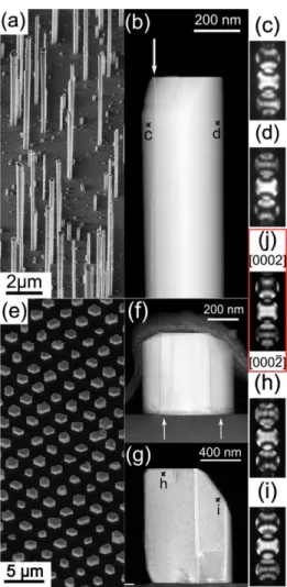
directions on the experimental patterns and consequently to deduce the nanostructure polarities.Figure 1 presents the SG and SAG of GaN nanostructures grown on c-sapphire
substrates. Fig. 1(a) shows a 45°-tilted SEM image of as-grown self-assembled GaN
wires. These wires grow vertically along the c-axis in epitaxy with the substrate.3 Fig.
1(b) shows a STEM image of a representative wire where two different regions separated
by an inversion domain boundary (IDB, indicated by the white arrow) are observed: one
with a flat top facet and the other with an inclined top facet at the wire edge. CBED
comparing the contrast inside the experimental disks with the simulation [Fig. 1(j)], it is
deduced that the small domain on the left side of the IDB with an inclined facet has a [0 0
0 1] growth direction (Ga-polarity), whereas the main domain on the right side with a flat
top surface exhibits a [0001 ] growth direction (N-polarity) in agreement with the
nitridated surface preparation.12 This behavior tends to show that N-polar crystals favor
the wire geometry formation with vertical sidewalls, while Ga-polar crystals present
inclined facets that may limit the vertical extension and in some extent may lead to the
formation of pyramidal geometry. The longitudinal change of polarity can not occur
spontaneously during the crystal growth (except using heavily Mg-incorporation15). Thus,
the polarity of GaN crystal is probably imposed by the nucleation seeds, which are
related to the surface state, i.e. to the thin in situ deposited SiNx layer or to the thin AlN
layer formed during the sapphire surface nitridation.3Erreur ! Signet non défini. To verify this
assumption, we performed SAG on patterned c-sapphire substrates using a thicker Si3N4
layer to position precisely the mask and to identify its influence on the crystal polarity.
Short growth duration (200 s) was chosen for SAG to obtain only the GaN-wire nucleation seed array [see Fig. 1(e)]. Three areas are observed by STEM on the typical
as-grown seed shown in Fig. 1(f): a central part with a flat top surface surrounded by two
crystals with inclined facets. The size of the central part is around 400 nm (i.e. the
diameter of the patterned holes). Two vertical IDBs are located close to the mask edge
opening (indicated by white arrows in Fig. 1(f)). An ion-milled seed [Fig. 1(g)] was
analyzed by CBED showing that the flat top crystal is N-polar [Fig. 1(h)] while the
GaN crystals correlated to the nature of the surfaces: Ga-polar crystal is preferentially
formed on SiNx mask and N-polar crystal on AlN/c-sapphire surface.
Based on these results concerning the shape dependence on the polarity, we then
performed a standard SG growth of GaN nanostructures directly on N-polar c-GaN
freestanding substrates to get the wires geometry. The same growth on Ga-polar substrate
was carried out for comparison. The 45°-tilted SEM images of as-grown samples on
N-polar and Ga-N-polar surfaces are shown in Fig. 2(a) and (f) showing the impact of the
substrate polarity on the crystal growth shapes. The nanostructure polarities were checked
by CBED taking into account the simulation references given in Fig. 2(k) and (l)
corresponding to the observed area thicknesses [Fig. 2(b) and (g)]: the growth on N-polar
GaN [Fig. 2(e)] exhibits N-polar wires [Fig. 2(d)],16 whereas the growth on Ga-polar
GaN [Fig. 2(j)] exhibits Ga-polar pyramidal shape nanostructures [Fig. 2(h) and (j)]. As
expected, the polarity is maintained between the substrate and the nanostructures as it is
schematized in Fig. 3 (a) and (c).
The kinetic Wulff’s plots (ν-plot) giving the growth velocities along different
orientations are usually used to describe the MOVPE growth features to take into account
non equilibrium phenomena.17,18 Recently, the GaN non-equilibrium shapes obtained by
MOVPE have been measured or calculated for different growth conditions on polar,19
semipolar and nonpolar20,21surfaces. The anisotropy of the growth rate along <0 0 0 1>
coming from the crystal polarity has been pointed out without mentioning the influence
of the substrate polarity. Our present results allow obtaining the schematic representation
of the ν-plot considering the substrate polarity effect (see Fig. 3 (b) and (d) where the
[0001 ] and <1010 > are in agreement with literature, and the relative observed
velocities lead to c-oriented wires with {1010}-sidewalls. For Ga-polar GaN, the
0001
and <1010> cusps are not observed, but rather the <101n> giving the pyramidal shape
(n=1,3… depending on local growth conditions).
Optical properties of as-grown pyramidal and wire-shaped nanostructures were
measured at room temperature by photoluminescence (PL) excited with a 244 nm laser
beam usingthe same experimental conditions (see Fig. 4 (a)). The optical property of the
as-grown GaN wires is better than the pyramidal shaped nanostructures without a
defect-related yellow band (YB) luminescence. In order to rule out the signal coming from the substrate, μ-PL was also made on single GaN wires at room temperature (see Fig. 4 (b)).
The spectrum shows a good near band edge emission peak at 351 nm without YB
indicating the high crystal quality of the wires.
In summary, we have shown that the N-polar wire growth is determined by the
substrate polarity in the case of homoepitaxy. Growths on c-sapphire and freestanding
GaN substrates evidenced that an N-polar surface leads to wire shape, whereas a Ga-polar
one leads to pyramidal shapes. This shape selection method gives a novel approach to
grow by MOVPE catalyst-free high crystal quality GaN wires showing good optical
properties. It may be generalized to many other systems to get nanowires using other
growth techniques combined with polarity-controlled substrates.
The authors would like to highlight the role of G.P.M. to initiate this study, J. Dussaud
and M. Lafossas for technical support, B. Martin, S. Landis, F. Levy and P. Gilet from
acknowledges P.-H. Jouneau and G. Feuillet for scientific support and X.J.C. for the
financial support of the foundation « Nanosciences aux limites de la Nanoélectronique ».
The work was partly funded by the French ANR Bonafo (ANR-08-Nano-031-01) and
References
1
R.X. Yan, D. Gargas, and P.D. Yang, Nature Photonics 3, 569 (2009).
2
T. Kuykendall, P. Pauzauskie, S.W. Lee, Y.F. Zhang, J. Goldberger, and P.D. Yang,
Nano Lett. 3, 1063 (2003).
3
R. Koester, J.S. Hwang, C. Durand, L.S. Dang, and J. Eymery, Nanotechnology 21,
015602 (2010).
4
H. Sekiguchi, K. Kishino, and A. Kikuchi, Appl. Phys. Lett. 96, 231104 (2010).
5
K. Tachibana, T. Someya, S. Ishida, and Y. Arakawa, Appl. Phys. Lett. 76, 3212
(2000).
6
P. R. Edwards, R. W. Martin, I. M. Watson, C. Liu, R. A. Taylor, J. H. Rice, J. H. Na, J.
W. Robinson, and J. D. Smith, Appl. Phys. Lett. 85, 4281 (2004).
7
S.D. Hersee, X.Y. Sun, and X. Wang, Nano Lett. 6, 1808 (2006).
8
M. Aoki, H. Yamane, M. Shimada, T. Kajiwara, S. Sarayama, and F. J. DiSalvo, Cryst.
Growth Des. 2, 55 (2002).
9
D. Cherns, L. Meshi, I. Griffiths, S. Khongphetsak, S. V. Novikov, N. Farley, R. P.
Campion, and C. T. Foxon, Appl. Phys. Lett. 92, 121902 (2008).
10
S. H. Lee, T. Minegishi, J. S. Park, S. H. Park, J.-S. Ha, H.-J. Lee, H.-J. Lee, S. Ahn, J.
Kim, H. Jeon, and T. Yao, Nano Lett. 8, 2419 (2008).
11
Standard notations are used for polarity: a positive direction of the bond pointing from
the Ga cation to the N anion defines the polar axis c labeled [0001] called also Ga-polar
orientation.
12
F. Liu, R. Collazo, S. Mita, Z. Sitar, G. Duscher, and S. J. Pennycook, Appl. Phys.
13
The diffraction patterns were carefully oriented in relation to the images: the sample
was slightly lowered to be over-focused in diffraction mode to obtain a shadow image in
the diffraction disks without any 180° rotation. For a given thickness, dynamical
scattering induces different contrasts inside the [0002] and the [0002 ] disks.
14
P. A. Stadelmann, JEMS Electron Microscopy Software (java version 1.3422W2003),
CIME-EPFL, Switzerland, 1999–2003.
15
V. Ramachandran, R. M. Feenstra, W. L. Sarney, L. Salamanca-Riba, J. E. Northrup,
L. T. Romano, and D. W. Greve, Appl. Phys. Lett. 75, 808 (1999).
16
In the case of growth on N-polar GaN and as mentioned for SG on sapphire, some
Ga-polar crystals are observed due to nucleation on the SiNx layer [Fig. 2(c)].
17
G. Wulff, Z. Krystalloger, Mineral. 34, 449 (1901).
18
J. E. Taylor, J. W. Cahn, and C. A. Handwerker, Acta Metall. Mater. 40, 1443 (1992).
19
D. Du, D. J. Srolovitz, M. E. Coltrin, and C. C. Mitchell, Phys. Rev. Lett. 95, 155503
(2005).
20
Q. Sun, C. D. Yerino, T. S. Ko, Y. S. Cho, I.-H. Lee, J. Han, and M. E. Coltrin, Appl.
Phys. Lett. 104, 093523 (2008).
21
Figures
FIG. 1. (Color online) Self-assembled growth (SG) of GaN wires on c-sapphire. (a)
45°-tilt SEM view and (b) STEM image of a single wire. Selective area growth (SAG) of a
wire seed array: (e) 45°-tilt SEM view and (f, g) STEM images of single seeds.
Experimental CBED patterns of the points marked c, d and h, i in (b) and (g) are given in
(c), (d) and (h), (i) respectively. As a reference, the simulated CBED pattern14 for 110 nm
thickness is given in (j). CBED patterns show Ga-polarity of the domains with inclined
FIG. 2. (Color online) Self-assembled growth of GaN wires on N-polar GaN: (a) 45°-tilt
SEM view, (b) STEM image of a single wire. Experimental CBED patterns showing (c)
Ga polarity of the domain with an inclined facet (marked c), (d) N polarity of the one
with a horizontal facet (marked d), and (e) N polarity of the GaN substrate.
Self-assembled growth of GaN pyramids on Ga-polar GaN: (f) 45°-tilt SEM view, (g) STEM
image. Experimental CBED patterns showing Ga polarity of (h) big pyramids, (i) small
pyramids, and (j) the GaN substrate. As references, the simulated CBED patterns14 for
FIG. 3. (Color online) Schematics of the GaN nanostructure shape selection for growths
on (a) N-polar and (c) Ga-polar GaN. The corresponding kinetic Wulff’s plots map on the
1120
plane are given in (b) and (d): dots correspond to observed planes and dotted linesare extrapolated velocity values.
FIG. 4. (Color online) Room temperature (300 K) photoluminescence (PL) spectra of (a)
as-grown pyramids and wires on GaN freestanding substrates having respectively the Ga-