50-nm E-mode In[subscript 0.7]Ga[subscript 0.3]As PHEMTs
on 100-mm InP substrate with f[subscript max] > 1 THz
The MIT Faculty has made this article openly available.
Please share
how this access benefits you. Your story matters.
Citation
Kim, Dae-Hyun et al. “50-nm E-mode In[subscript 0.7]IEEE
International Electron Devices Meeting (IEDM), 2010. 30.6.1–30.6.4.
© Copyright 2010 IEEE
As Published
http://dx.doi.org/10.1109/IEDM.2010.5703453
Publisher
Institute of Electrical and Electronics Engineers (IEEE)
Version
Final published version
Citable link
http://hdl.handle.net/1721.1/73128
Terms of Use
Article is made available in accordance with the publisher's
policy and may be subject to US copyright law. Please refer to the
publisher's site for terms of use.
50-nm E-mode In
0.7Ga
0.3As PHEMTs on 100-mm InP substrate with f
max> 1 THz
Dae-Hyun Kim, *Jesús A. del Alamo, Peter Chen, Wonill Ha, Miguel Urteaga and Berinder Brar
Teledyne Scientific Company (TSC), Thousand Oaks, CA 91360, USA, E-mail: dkim@teledyne.com *Massachusetts Institute of Technology (MIT), Cambridge, MA 02139, U.S.A
Abstract
We have demonstrated 50-nm enhancement-mode (E-mode)
In0.7Ga0.3As PHEMTs with fmax in excess of 1 THz. The
devices feature a Pt gate sinking process to effectively thin down the In0.52Al0.48As barrier layer, together with a two-step recess process. The fabricated device with Lg = 50-nm exhibits VT = 0.1 V, gm,max = 1.75 mS/μm, fT = 465 GHz and fmax = 1.06 THz at a moderate value of VDS = 0.75 V. In addition, we have physically modeled the abnormal peaky behavior in Mason’s unilateral gain (Ug) at high values of VDS. A revised small
signal model that includes a shunting Rgd-NDR with negative
value successfully describes the behavior of the device from 1
to 67 GHz. .
Introduction
The last few years have witnessed an explosion of interest in devices suitable for ultra high frequency applications, such as in the Tera-Hz regime. To accomplish this, a device technology must rely on boosting high frequency operation by
reducing gate length (Lg) to sub-50 nm, improving carrier
transport in the channel, improving electrostatic integrity and minimizing resistance and capacitance parasitics [1-2].
An additional feature that is highly desirable in future THz
circuits is a positive VT. Achieving E-mode PHEMTs is rather
difficult as it demands tight control of tins, especially as Lg approaches to sub-50 nm regime. In this work, we use Pt gate sinking to shift VT and to thin down the barrier [3]. Pt gate sinking in devices with high InAs compositions in the channel have been demonstrated before [4-5]. What is important in this work is a well balanced device design that pays close attention to short-channel effects and that leads to exceptional high frequency characteristics. In this work, we demonstrate for the
first time enhancement-mode In0.7Ga0.3As PHEMTs with fmax
in excess of 1 THz at a moderate value of VDS = 0.75 V.
Process Technology
Fig. 1 shows a cross section of the device structure. The
device architecture brings together unique features designed to minimize parasitics and mitigate short-channel effects, as in [5]. The epitaxial layer structure is similar to [6]. It features a
10-nm thick In0.7Ga0.3As channel. After a two-step recess
process that exposes an InAlAs barrier, a Pt/Ti/Pt/Au (3/30/10/350 nm) gate was created. Subsequently, the devices were annealed at 250 °C for 2 minutes to drive the Pt into the InAlAs barrier. In this way, a gate-to-channel distance (tins) of
about 4-nm was achieved with side-recess spacing (Lside) of
150-nm. A range of gate length (Lg) in this work was from
200-nm to 50-nm. S Cap D Etch stopper Barrier Channel Buffer tins Oxide Lside tch Buried Pt 100 mm InP Substrate
Fig. 1 Schematic of In0.7Ga0.3As PHEMT on a 100-nm InP substrate. It features tch = 10 nm and tins = ~ 4 nm. The devices were fabricated with Pt gate sinking. The smallest Lg was 50-nm, and Lside was 150-nm.
DC & Microwave Characteristics
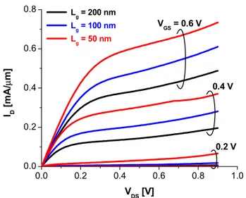
Fig. 2 shows typical DC output characteristics of
In0.7Ga0.3As PHEMTs with various values of Lg.
Well-behaved drain current saturation is observed with excellent pinch-off characteristics up to VDS = 0.9 V for all gate lengths.
Typical ON-resistance (RON) is about 0.4 Ω-mm for Lg = 50
nm devices. As in the author’s previous work on In0.7Ga0.3As PHEMTs [5], the devices in this work also show improved current driving capability as Lg scales down to 50 nm.
Fig. 3 plots the transconductance (gm) characteristics of the
same devices at VDS = 0.5 V. The devices exhibit a
continuously increasing gm, as Lg scales down to 50-nm.
Particularly, the device with Lg = 50 nm shows gm,max = 1.7 S/mm. These outstanding characteristics arise from improved charge control behavior through the combination of the two-step recess plus buried Pt gate sinking technology.
Fig. 4 plots the sub-threshold and transfer characteristics
of all the 50-nm In0.7Ga0.3As PHEMTs on a 100-mm wafer.
The devices offer a true e-mode operation (VT = 0.1 V,
defined with a criteria of ID = 1 mA/mm) with excellent VT
uniformity (ΔVT = 28 mV) across the wafer. Besides, the
devices show very sharp subthreshold characteristics, as assessed by a subthreshold-swing = 80 mV/dec and DIBL = 80 mV/V, which are close to those of advanced InGaAs PHEMTs [6]. Besides, these devices do not show excessive gate leakage current. The typical gate turn-ON voltage
(Vg,ON) was greater than 0.5 V with a criteria of Ig = 1
0.0 0.2 0.4 0.6 0.8 1.0 0.0 0.2 0.4 0.6 0.8 0.2 V ID [mA/ μ m] VDS [V] Lg = 200 nm Lg = 100 nm Lg = 50 nm VGS = 0.6 V 0.4 V
Fig. 2 Output characteristics of In0.7Ga0.3As PHEMTs with various gate lengths (Lg = 200, 100 and 50 nm).
0.0 0.2 0.4 0.6 0.0 0.5 1.0 1.5 2.0 L g = 200 nm Lg = 100 nm Lg = 50 nm g m [m S/ μ m] VGS [V] VDS = 0.6 V
Fig. 3 Transconductance (gm) characteristics for In0.7Ga0.3As PHEMTs with various gate lengths at VDS = 0.5 V.
0.0 0.2 0.4 0.6 10-8 10-7 10-6 10-5 10-4 10-3 VDS = 0.5 V ID [A / μ m] VGS [V] 0 0.8 ID [m A / μ m] 0.6 0.2 0.4
Fig. 4 Subthreshold and transfer characteristics of 50-nm
In0.7Ga0.3As PHEMTs on a 100-mm InP substrate at VDS = 0.5 V.
Microwave performance was characterized using an Agilent precision-network-analyzer (PNA) with a standard Line-Reflection-Reflection-Match (LRRM) calibration from 1 GHz to 67 GHz. On-wafer open and short structures were used to de-embed pad capacitances and inductances. Fig. 5 plots measured (symbols) and small-signal modeled (lines)
short-circuit current gain (H21), maximum stable gain (MSG),
Mason’s unilateral gain (Ug) and stability factor (k) for the 50-nm device at (a) VGS = 0.5 V and VDS = 0.5 V, and (b) VGS
= 0.5 V and VDS = 0.75 V. The transistor fT was determined
by extrapolating |H21| with a slope of -20 dB/decade using a
least-squares fit. The 50-nm PHEMT in this work exhibits a
high value of fT = 465 GHz at VDS = 0.75 V, and over 400
GHz at VDS = 0.5 V. More significantly, the device displays
an extremely high value of maximum oscillation frequency (fmax). At VDS = 0.75 V, fmax of 1.06 THz is obtained from extrapolation using the measured Ug.
109 1010 1011 1012 0 10 20 30 40 50 Ug MSG H21 Frequency [Hz] Ga in s [d B] Lines: Modeled Scatters: Measured k 0 1 2 3 4 5 St ab il ity F ac to r (k) (a) VGS = 0.5 V and VDS = 0.5 V 109 1010 1011 1012 0 10 20 30 40 50 Ug MSG H21 Frequency [Hz] Ga ins [ dB] Lines: Modeled Scatters: Measured k 0 1 2 3 4 5 Sta b ility Fact or (k) (b) VGS = 0.5 V and VDS = 0.75 V
Fig. 5 RF gains (H21, Ug and MSG), stability factor (k), and S-parameters (inset) for 50-nm In0.7Ga0.3As PHEMTs with Wg = 2 x 20 μm vs. frequency, together with predictions from the small-signal model. Inset of both figures is the comparison of measured and modeled S-parameters.
S11 S22 S21/10 10xS12 S11 S22 S21/10 10xS12 VDS = 0.5 V 30.6.2 IEDM10-693
To accurately extract the value of fmax, we carried out small-signal modeling at different bias conditions, as recently proposed [7]. The estimated fmax is sensitive to the values of small-signal parameters, such as Rg, Rs and Rd. To make the small-signal modeling process robust, we carefully extracted all the parasitic resistances [7], used them to derive all the intrinsic parameters, and finally verified the accuracy of the small-signal model at different bias conditions across multiple devices. As shown in Fig. 5, our models predict all the S-parameters, RF gains and k consistently at both bias conditions.
From the model, the 50-nm device yields fmax = 1.08 THz at
VDS = 0.75 V, which is very similar to the value from the
measured Ug. This is the highest fmax ever reported in any FET on any material system with E-mode operation.
Increasing VDS beyond 0.75 V is likely to yield even better fmax. However, it is very difficult to extract it from either the
experimental measurement of Ug, or from the small-signal
model. This is because Ug is apt to show sharp peaky
behavior at intermediate frequencies as VDS increases. Fig. 6
shows measured and modeled RF gains and k at VDS = 0.9 V.
Indeed, Ug exhibits an anomalously increasing behavior with
frequency, and the modeled Ug fails to describe it. For a
given device, we have verified that this behavior is reproducible across different measurement systems. Such behavior has also been observed in high frequency devices by another group [1]. 109 1010 1011 1012 0 10 20 30 40 Ug MSG H21 Frequency [Hz] Ga ins [ dB ] Lines: Modeled Scatters: Measured k 0 1 2 3 4 5 St ab ility Fa ctor (k )
Fig. 6 RF gains (H21, Ug and MSG), k-factor, and S-parameters (inset) for 50-nm In0.7Ga0.3As PHEMTs vs. frequency at VGS = 0.5 V and VDS = 0.9 V, together with model predictions.
Advanced Small-Signal Model
In trying to understand the abnormal behavior in Ug, we
found that Ug is actually negative before the peak occurs.
From the definition of Mason’s unilateral gain, Ug takes the
sign of its denominator. The expression of Ug is: Re(Y11) • Re(Y22) – Re(Y12) • Re(Y21)
| Y21– Y12|2
Ug= (1)
Fig. 7 shows the denominator of the experimental Ug for
the 50-nm device at VDS = 0.5 V and 0.9 V. Clearly, a
negative value of Ug arises from its denominator and this
occurs at high values of VDS. Furthermore, the frequency at
zero-crossing in Den(Ug) is responsible for the abnormal
peaky behavior in Ug. Now, the question arises: what is the
origin of this? We found that a ‘Negative-Differential-Resistance’ (NDR) effect between gate and drain at high values of VDS is responsible for the negative Ug.
109 1010 1011 1012 -40.0µ -20.0µ 0.0 20.0µ 40.0µ 60.0µ VDS = 0.5 V VDS = 0.9 V De n o m ina to r of Ug Frequency [Hz] zero-crossing
Fig. 7 Denominator of Ug for 50-nm device as a function of frequency at VDS = 0.5 V and 0.9 V.
A possible mechanism for this is shown in Fig. 8. As VDS
increases, high-field effects at the drain-side of the gate, such as hot electron production, become more prevalent. These hot electrons are capable of causing NDR effects between the
gate and drain [8]. Fig. 9 shows the measured IG as a
function of VDS for 50-nm devices with different values of
VGS. As VDS increases, IG initially decreases (due to the reduction and eventual change of sign of the gate-drain gate leakage current), and then increases at VDS = 0.5 V for VGS > 0.4 V due to real-space transfer of hot electrons from the channel into the gate [7]. This is a region of negative differential resistance in IG. VGS> 0 V High V DS e -Drain Cap. Barrier Channel Source Forward e -injection Hot e -transfer Reverse e -leakage IG
Fig. 8 Physical origin of NDR effect between gate and drain.
As VDS increases, there is real-space transfer of hot electrons from the chanbnel to the gate.
S11
S22
S21/10
Fig. 9 IG vs. VDS for 50-nm device at various values of VGS. From the RF point of view, this phenomenon can be
modeled by adding a shunt negative resistance (Rgd-NDR)
between gate and drain, as shown in Fig. 10. From this model, the denominator of Ug is approximated as g0/Rgs + gm/Rgd,total. If Rgd_total has a negative sign and its absolute value is smaller than gmRgs/g0, then the denominator of Ug becomes negative. We have used this revised small-signal model to estimate fmax. The value of Rgd_total can be obtained from Re(Y12) = -Rgd_total in the equivalent circuit model. Fig. 11 plots measured and
modeled RF gains and k at VDS = 0.9 V with the addition of
Rgd-NDR. Our model predicts the experimental gain
characteristics and the k-factor very nicely, including the sharp peak in Ug. Using the model, we extrapolated a value of fmax = 920 GHz at VDS = 0.9 V, which is a bit lower than that
at VDS = 0.75 V. This is likely due to the drop in fT that
results from the increase in the drain delay as VDS increases. To see how our devices stand out in comparison to other reports, Fig. 12 plots fmax as a function of fT for our 50-nm
device with VDS = 0.75 V, as well as other reports including
III-V HBTs and III-V HEMTs. Clearly, the device in this work exhibits a record value of fmax for e-mode operation.
Cgs Cgd υ gmiυ Ri goi Cds Rgs Rgd Rgd-NDR G’ S’ D’
Fig. 10 Modified small-signal equivalent circuit of the
intrinsic device with the shunt addition of Rgd_NDR between
intrinsic gate and drain. Rgd_total-1 is the sum of Rgd_NDR-1 and Rgd-1, and Re(Y12) is - Rgd_total.
109 1010 1011 1012 0 10 20 30 40 Ug MSG H21 Frequency [Hz] Gain s [ d B]
Lines: Modeled with NDR Scatters: Measured k 0 1 2 3 4 5 Stab ilit y F acto r (k)
Fig. 11 Data and modified model predictions for RF gains and
k-factor at VGS = 0.5 V and VDS = 0.9 V. Our model predicts the abnormal behavior in Ug nicely, as well as the k-factor.
0 200 400 600 800 1000 0 500 1000 1500 MIT HEMT Fujitsu HEMT NGST HEMT SNU HEMT UCSB HBT UIUC HBT Postech HBT HRL HBT ETH HBT max f fτ fma x [G H z] fT [GHz] 300 600 700 = favg = TSC (This work)
Fig. 12 fmax as a function of fT for 50 nm In0.7Ga0.3As PHEMTs in this work, as well as other reports on III-V HEMTs and HBTs. For all the data fT and fmax are measured at the same bias condition.
Conclusions
In summary, we have demonstrated for the first time 50-nm
E-mode InGaAs PHEMTs on a 100-mm InP substrate with fmax
> 1 THz. We have physically modeled the abnormal peaky behavior in Ug at high values of VDS, and successfully revised the small signal model by adding Rgd-NDR with negative value. Without doing this, any attempt on fmax extrapolation at high values of VDS could result in an over-estimation on its value.
References [1] R. Lai et al., IEDM, p. 609, 2007.
[2] D.-H. Kim et al., IEEE EDL, p. 830, 2008.
[3] Mahajan et al., IEEE EDL, p. 284, 1997.
[4] T.-W. Kim et al., IEEE TED, p. 1577, 2008.
[5] D.-H. Kim et al.., IEDM, p. 719 , 2008.
[6] D.-H. Kim et al., IEEE TED, p. 2606 , 2007.
[7] D.-H. Kim et al., DRC, late news paper, 2010.
[8] S.J. Kim et al., JJAP, p. 6152 , 2000.
Acknowledgements
This work was sponsored in part by DARPA under a SPAWAR System Center, San Diego Contract Number N660001-06-C-2025. The authors thank Nidhi and U. Mishra for the help in doing S-parameter measurements, and A. Lui with IQE for the growth of the epi wafer.
0.0 0.2 0.4 0.6 0.8 1.0 10-8 10-7 10-6 10-5 0.3 V 0.4 V 0.5 V IG [A / μ m] VDS [V] VGS = 0.6 V NDR (G-D) 30.6.4 IEDM10-695
![Fig. 1 shows a cross section of the device structure. The device architecture brings together unique features designed to minimize parasitics and mitigate short-channel effects, as in [5]](https://thumb-eu.123doks.com/thumbv2/123doknet/13806904.441497/2.918.549.778.224.470/section-structure-architecture-features-designed-minimize-parasitics-mitigate.webp)