HAL Id: hal-02011620
https://hal.univ-lorraine.fr/hal-02011620
Submitted on 8 Feb 2019
HAL is a multi-disciplinary open access
archive for the deposit and dissemination of
sci-entific research documents, whether they are
pub-lished or not. The documents may come from
L’archive ouverte pluridisciplinaire HAL, est
destinée au dépôt et à la diffusion de documents
scientifiques de niveau recherche, publiés ou non,
émanant des établissements d’enseignement et de
Telecommunication Wavelength with Zero Applied
Magnetic Field
Abdelhak Djeffal, Fabian Cadiz, Mathieu Stoffel, Delphine Lagarde, Xue Gao,
Henri Jaffrès, Xavier Devaux, Sylvie Migot, Xavier Marie, Hervé Rinnert, et
al.
To cite this version:
Abdelhak Djeffal, Fabian Cadiz, Mathieu Stoffel, Delphine Lagarde, Xue Gao, et al.. Co Fe
-B / Mg O / Ge Spin Photodiode Operating at Telecommunication Wavelength with Zero Applied
Magnetic Field. Physical Review Applied, American Physical Society, 2018, 10 (4),
�10.1103/physre-vapplied.10.044049�. �hal-02011620�
Co-Fe-B/MgO/Ge Spin Photodiode Operating at Telecommunication Wavelength
with Zero Applied Magnetic Field
Abdelhak Djeffal,1Fabian Cadiz,2Mathieu Stoffel,1,*Delphine Lagarde,2Xue Gao,1Henri Jaffrès,3
Xavier Devaux,1Sylvie Migot,1Xavier Marie,2Hervé Rinnert,1Stéphane Mangin,1
Jean-Marie George,3Pierre Renucci,2,†and Yuan Lu1,‡
1Université de Lorraine, Institut Jean Lamour, UMR CNRS 7198, campus ARTEM, 2 Allée André Guinier, 54011
Nancy, France
2Université de Toulouse, INSA-CNRS-UPS, LPCNO, 135 avenue de Rangueil, 31077 Toulouse, France 3Unité Mixte de Physique, CNRS, Thales, Univ. Paris-Sud, Université Paris-Saclay, 91767 Palaiseau, France
(Received 24 April 2018; revised manuscript received 2 August 2018; published 19 October 2018) We report on the growth and study of Co-Fe-B/MgO/Ge(001) spin photodiode by using a combination of both molecular beam epitaxy (MBE) and sputtering methods. An epitaxial growth of MgO on Ge in MBE is achieved by the deposition of MgO at room temperature (RT) followed by a post-growth anneal-ing at 300 °C. The spin detector, which consists of 1.1-nm ultrathin Co-Fe-B layer capped with 5-nm Ta is subsequently grown by sputtering at RT. After a post-growth annealing of the whole structure at 250 °C, we obtain clear evidence of a strong perpendicular magnetic anisotropy in the temperature range 10-300 K. Co-Fe-B/MgO/Ge(001) heterojunctions are then processed into spin photodiodes demonstrat-ing at zero magnetic field a photocurrent helicity asymmetry of about 0.9% at 9 K and 0.1% at RT at the telecommunication wavelength of 1310 nm. The demonstration of a spin photodiode working at a telecommunication wavelength with zero applied magnetic field is of great interest for future applications of the optical transport of spin information.
DOI:10.1103/PhysRevApplied.10.044049
I. INTRODUCTION
The evolution of microelectronics is guided by Moore’s law, which will soon be confronted with fundamental phys-ical limits, thus hampering future developments. For this reason, alternative device concepts exploring new func-tionalities have been envisioned. Among these, devices that exploit the spin as a new degree of freedom instead of, or in addition to the electron charge, could lead to great benefits. This has led to the birth of a new and very rapidly growing research field called spin-electronics or spintronics [1]. When spintronics is associated with semiconductors, hybrid devices which integrate both ferro-magnetic materials and semiconductor materials onto the same chip can be envisioned. This will be of particular interest since all operations such as storing and processing of information could then be integrated within one technol-ogy [2]. Remarkable successes have been achieved in this field during the last decade with different semiconductor materials [3–6]. One of the important achievements is the spin injection from a ferromagnetic contact into a semicon-ductor overcoming the resistance mismatch by inserting
*mathieu.stoff[email protected] †[email protected] ‡[email protected]
a thin oxide tunnel barrier at the metal/semiconductor interface [7]. Moreover, the development of spin-polarized light-emitting diodes (spin-LEDs) in which spin-polarized electrons are electrically injected into the active region of a semiconductor where they recombine radiatively with unpolarized holes to emit right- or left-circularly polar-ized light is of prime importance. It was found that the ferromagnetic spin injector plays a key role in determin-ing the efficiency of the spin injection [8,9]. In most cases, the spin-LED was studied in III-V-based semicon-ductors such as GaAs [10–14] or GaN [15–17]. How-ever, the reverse process: a spin photodiode [18], i.e., the electrical detection of a spin-polarized current when a ferromagnetic/insulator/semiconductor heterojunction is illuminated by a circularly polarized light has gained much less attention. Hirohata et al. [19] investigated the spin-dependent electron transport at the interface between NiFe and n-doped GaAs(110). They reported a 1% rel-ative variation of the photocurrent at room temperature (RT). Taniyama et al. [20] studied spin transport across Fe/GaAs(001) and Fe/AlOx/GaAs(001) heterojunctions.
The photocurrent variation was found to be strongly dependent on the applied magnetic field and reaches a maximum of 1.7% at RT. Hövel et al. [21] realized a pho-todetector using a p-i-n diode with a GaAs quantum well in the active region and a Fe/Tb multilayer on top of a MgO
layer to ensure filtering of the spin-polarized current at zero external magnetic field. The authors obtained a relatively large photocurrent helicity asymmetry of 3% at RT and in remanence. More recently, in order to avoid the use of an external magnetic field, Roca et al. [22] and Zhu et al. [23] have reported the possibility to operate under an oblique incident angle using in-plane magnetic injectors on top of the semiconductor part of the device.
While most previous studies of spin photodiodes have mainly focused on the GaAs-based semiconductor mate-rial, more recently, germanium (Ge) has also emerged as a promising material for spintronics due to its rather large spin-orbit coupling [24] and long electron-spin life-times [25]. Electrical spin injection, transport, and detec-tion has been studied experimentally in bulk Ge [5,26]. Very recently, fully epitaxial Fe/MgO/Ge(001) spin pho-todiodes were experimentally demonstrated showing a net photocurrent variation of about 5% when being excited at 0.95 eV (i.e., 1300 nm) with a 100% circularly right-and left-polarized light [27,28]. The key advantage here, compared to previous GaAs-based spin photodiodes proof-of-concepts, lies in the wavelength range corresponding to the telecommunication wavelength. In order to fulfill the optical selection rules [29], the magnetization needs to be out-of-plane. For this purpose, Rinaldi et al. [28] applied an external magnetic field of up to 1.2 Tesla to drive the magnetization of the 10-nm-thick Fe layer to the out-of-plane configuration. However, this appears to be a strong limitation for future practical device applica-tions. Moreover, the Zeeman effect due to a large magnetic field could also complicate the data analysis [30]. There-fore, a layer structure exhibiting a perpendicular magnetic anisotropy (PMA) would be highly desirable. Further-more, in order to get a sensitive photodetector and to minimize spurious effects such as the magnetic circular dichroism (MCD) effect, one should also minimize the light absorption in the top magnetic layer of the photodi-ode. To this aim, a magnetic spin detector with a thickness close to one nanometer would be of great interest. The demonstration of the growth of such an ultrathin mag-netic spin detector presenting a PMA on Ge for a zero applied magnetic field spin photodiode is, however, still lacking.
In this paper, we investigate the growth and spin-polarized photocurrent properties of an ultrathin Co-Fe-B/ MgO spin detector on Ge(001) substrates. We demonstrate that a careful tuning of the growth parameters and post-growth annealing conditions allows us to obtain a spin detector with strong perpendicular magnetic anisotropy in the range 10–300 K. Finally, encouraging results concern-ing Co-Fe-B/MgO/Ge(001) spin photodiodes operatconcern-ing at zero magnetic field are obtained: a photocurrent helic-ity asymmetry of about 0.9% is measured at 9 K and is still detectable (about 0.1%) at RT at the telecom-munication wavelength of 1310 nm. The demonstration
of a spin photodiode working at a telecommunication wavelength and with a zero applied magnetic field is of great interest for future applications on the optical transport of spin information [31].
II. EXPERIMENTAL DETAILS
Nominally undoped Ge(001) substrates (resistivity >50 ! cm) are used in this study. The ex-situ cleaning of the Ge(001) substrates is checked by atomic force microscopy (AFM) prior to their transfer into the molec-ular beam epitaxy (MBE) chamber. After in situ deoxida-tion, 2 nm of MgO are deposited at RT and subsequently annealed at 300 °C for 1 h. The growth is character-ized in situ by reflection high-energy electron diffraction (RHEED). The sample is then transferred without vac-uum breaking into the sputtering chamber where 0.5 nm MgO is deposited prior to the growth of a 1.1-nm-thick Co40Fe40B20 layer at RT. The heterostructure is finally
capped by a 5-nm-thick Ta layer. Ex situ annealing is per-formed using a rapid thermal annealing (RTA) oven under an argon atmosphere at 250 °C for 3 min [14]. The mag-netic properties are measured by superconducting quantum interference device (SQUID) magnetometry as a function of temperature in the range 10–300 K.
High resolution scanning transmission electron micro-scopy (HR-STEM) is performed to characterize the inter-facial structure using a probe-corrected JEOL ARM 200 CF operated at 200 kV. High-angle annular dark-field (HAADF) and bright-field (BF) images are simultaneously recorded. Electron energy loss spectroscopy (EELS) maps are recorded with a Gatan Quantum Imaging filter. In order to be able to correct energy drift and estimate the local thickness, the zero loss and the core loss spectra are simul-taneously recorded for a dispersion of 1 eV (Dual EELS method). The pixel size of spectrum images (SI) is typ-ically fixed between 0.1 and 0.15 nm. After energy drift correction, the SI are denoised using a principal compo-nent analysis method before quantitative analysis. The SI denoising is performed with the multi-statistical analysis plugins for Digital Micrograph “temDM” [32].
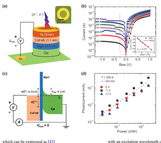
Spin photodiodes based on Co-Fe-B/MgO/Ge(001) heterojunctions are processed using standard UV pho-tolithography and Ar+ ion milling. First, circular mesas
with a diameter of 400 µm are defined [inset of Fig.4(a)]. Then, a second lithography step is used to define both ring-shaped top contacts and the bottom contacts. 150-nm Au/10-nm Ti are deposited as contact materials. Pho-tocurrent measurements are performed at normal incidence under an optical excitation provided by laser diodes (wave-length 980 nm or 1310 nm). The beam is focused onto the sample with a f = 20-mm lens (spot diameter of 2.5 µm). The laser power is about 1 mW. The helic-ity of the laser is modulated between right (σ+) and left
(σ−) circularly polarized light at 50 kHz by a
photoelas-tic modulator (PEM), and the corresponding photocurrent intensities Iσ+ and Iσ− are transformed into a voltage
with a transimpedance amplifier (gain 105) and detected
with a lock-in amplifier. A magnetic field perpendicular to the photodiode is generated by a coil inserted inside a vibration-free closed-cycle cryostat where the sample is mounted.
III. RESULTS AND DISCUSSION
Prior to the growth, we first investigate the cleaning of the initial Ge(001) surface. Sun et al. [33] have suggested a method which combines one or more oxidation cycles in a diluted hydrogen peroxide solution followed by dissolu-tion of the oxide in a HCl soludissolu-tion. Following this method, we obtain a rms surface roughness of about 1.3 nm, which is still a rather large value. Figure 1(a)shows an AFM image obtained after dipping a Ge(001) wafer in a 10% HCl solution for 5 min. The rms surface roughness is shown to decrease to about 0.21 nm, which is typical for a planar Ge(001) surface. This substrate is then immediately transferred into the MBE chamber. After 1-h annealing at 500 °C, the RHEED pattern [Fig. 1(b)] measured along the ⟨110⟩ direction exhibits, in addition to the (−1,0) and (0,1) streaks, the typical half-order (−1/2,0) and (0,1/2) streaks. This indicates that deoxidation has occurred lead-ing to the well-known (2 × 1) reconstruction of the clean Ge(001) surface. We then deposit 2 nm MgO at RT onto the Ge(001)-(2 × 1) surface prior to annealing at 300 °C for 1 h. The RHEED patterns measured after annealing along the Ge ⟨100⟩ and ⟨110⟩ directions are shown in Figs.1(c)and 1(d), respectively. One can recognize that the patterns consist of streaks indicating that MgO grows epitaxially onto the Ge(001)-(2 × 1) surface. We note that when the growth of MgO is directly performed at 225 °C, streaks are no longer observed (not shown here) indicat-ing that the MgO film is polycrystalline. Interestindicat-ingly, if one considers the MgO RHEED pattern measured along the Ge⟨100⟩ direction [Fig.1(c)], one can distinguish two families of streaks pointed at by either green or red arrows. The streaks indicated with green arrows correspond to an epitaxial growth relationship of MgO[110]//Ge[100], i.e., with the MgO unit cell turned by about 45° with respect to the Ge unit cell [Fig.1(e)]. The streaks indicated with red arrows correspond to an epitaxial growth relationship of MgO[100]//Ge[100], i.e., with cube-on-cube growth of the MgO unit cell on the Ge unit cell [Fig. 1(f)]. Since the streaks pointed at by green arrows are more intense than those pointed at by red arrows, we can thus con-clude that MgO[110]//Ge[100] corresponds to the major growth direction. This is also the configuration which min-imizes the misfit strain (5.2%) and thus the elastic energy. The minority growth direction MgO[100]//Ge[100] corre-sponds to the configuration which maximizes the misfit
Major Minor
(a) (b)
(c) (d)
(e) (f)
rms = 0.21 nm
FIG. 1. (a) AFM image obtained for a cleaned Ge(001) sub-strate before being introduced into the MBE chamber. (b) RHEED pattern on a Ge(001)-(2 × 1) reconstructed surface mea-sured along the [110] direction. RHEED patterns meamea-sured after deposition of 2-nm MgO on Ge(001) at RT followed by anneal-ing at 300 °C for 1 h (c) along the Ge [100] direction and (d) along the Ge [110] direction. The green and red arrows in (c) indicate that the growth is textured with two different orienta-tions, either MgO [110]//Ge[100] [green arrows, major growth direction shown in (e)] or MgO[100]//Ge[100] [red arrows, minor growth direction shown in (f)].
strain (25.6%) and thus the elastic energy. This is con-sistent with previous observations by Petti et al. [34]. In fact, the majority growth direction can be explained by the lattice-matching epitaxy (LME) approach, while the minority growth direction agrees with the prediction of the domain-matching epitaxy (DME) approach [35]. The different growth directions are also determined by the interfacial energies related to chemical interactions [34]. After a 2-nm MgO growth, the sample is transferred to the sputtering chamber without vacuum breaking, where MgO(0.5 nm)/Co-Fe-B(1.1 nm)/Ta(5 nm) is deposited at RT.
We perform STEM EELS combined analyses on the as-grown sample to study the interfacial structure and to get
information on the local chemistry. As shown in Fig.2(a)
recorded with STEM HAADF mode at low magnification, the interfaces between the layers appear very sharp and the layers have constant thickness and low roughness. Because heavy atoms diffuse more electrons than lighter ones, the contrast in STEM HAADF images is linked to the square of the mean atom number. On this micrograph, the Ge sub-strate is located on the bottom of the image. The MgO layer appears in dark whereas the metal layers appear in white due to Ta. A thin gray layer with contrast close to that of Ge is visible at the interface between MgO and Ta indi-cating the localization of the Co-Fe-B layer. The granular structure on the top of the multilayer is characteristic of a PtC protective layer deposited during the FIB processing (Pt grains in an amorphous C matrix). Between the metal layers and the PtC capping, a gray layer appears. It indi-cates that the Ta capping is oxidized at its surface on about 30% of its thickness. The HR-STEM BF images shown in Fig.2(b)confirm the texture of the MgO layer observed by RHEED during the growth (Fig. 1) with MgO (001)//Ge (001). At the interface between the Ge substrate and the MgO layer [inset of Fig.2(b)], a phase (2- or 3-atom planes in thickness, pointed at by red arrow) appears with a local lattice constant different from that of MgO or Ge and with a perfect epitaxy on Ge. The nature of this thin layer (less than 0.5-nm thick) will be identified using the spatially resolved EELS mapping. Figure 2(c)shows the element
maps extracted from the quantitative analysis of an EELS spectrum image recorded in the area indicated by the red rectangle drawn on the STEM HAADF survey image [inset of Fig.2(d)]. The Ge substrate is presented on the top of the images. This analysis clearly shows that the interface between Ge and MgO is oxygen-rich. Figure2(d), consti-tuted with the superposition of GeL, CoL, MgK, and TaM
signals, allows to precisely localize and estimate the thick-ness of the oxidized Ge layer. The result of the quantitative analysis in this area gives a mean atom ratio of 34% Ge and 64% O, close to GeO2, without any other element. The
thickness deduced from the overall contrast in the oxygen map and from the superposed elemental map is estimated to be about 0.45 nm. This thickness is in total accordance with the 2- or 3-atom planes seen at the interface on BF micrographs [inset of Fig.2(b)]. This ultrathin GeO2layer
between Ge and the MgO could be formed during or after the growth of the MgO layer since the RHEED patterns show only a clean Ge surface before MgO growth. Further-more, the chemical maps allow to confirm the thickness of each deposited layer. MgO and Co-Fe-B layers appear to be 2.3- and 1.3-nm thick, respectively, from the EELS maps. Despite its thin thickness, the Co-Fe-B layer is con-tinuous with a very homogeneous thickness and sharp interfaces on both sides. The ferromagnetic layer is found to have a mean ratio of 55% Fe and 45% Co, which is a bit richer in iron than is expected. It has to be noted that
(a) (b)
(c)
(d)
FIG. 2. (a) Low magnification STEM HAADF image of the sample. The MgO layer appears in dark whereas the metal layers appear in white. The gray layer on the top of the multilayer indicates the Ta capping is partially oxidized. The granu-lar structure on the top of the multilayer is characteristic of a PtC protective layer deposited during the FIB processing. (b) HR- STEM BF image showing the good crystallinity of the MgO barrier. The zone axis of the Ge part is [001]. The arrow in the magnified inset points out the crys-talline GeO2 with 2 or 3 monolayers at the Ge/MgO interface. (c) Individual ele-ment maps extracted from quantitative analysis of EELS spectrum image (SI). (d) Superposed element map (Ge, Mg, Co, and Ta) precisely showing the distri-bution of elements at the interface. Inset: HAADF survey image shows where the SI is recorded. The Ge substrate is pre-sented on the top of the images. The contrast Ge signal is not clearly visible at the MgO-Ge interface due to the presence of oxidized Ge. The quantitative analysis yields 34% Ge and 64% O.
(a) (b)
(c) (d)
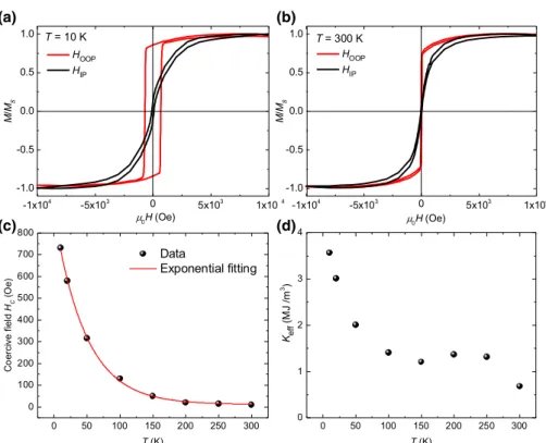
FIG. 3. M-H curves measured with the magnetic field applied either in-plane (HIP, black solid line) or out-of-plane (HOOP, red solid line) at (a) T = 10 K and (b)
T = 300 K. (c) The evolution of
the coercive field Hc with tem-perature. The experimental data are shown as black dots while the fitting using a single exponential decay is shown as a red solid line. (d) Evolution of the effective anisotropy constant with temper-ature as determined by the area method (see text).
even if boron is detected close to the Co-Fe-B/Ta inter-face, the signal is too weak for quantitative analysis with the STEM and spectrometer parameters chosen for this EELS mapping. Nevertheless, in our previous work on the EELS mapping of a Ta-capped Co-Fe-B/MgO spin injec-tor deposited on a spin LED, boron diffusion in the Ta layer was detected due to Co-Fe-B crystallization after anneal-ing [36]. As observed from the HAADF images, the Ta capping layer appears oxidized on the top of the surface for 2–3 nm. The atom ratio between Ta and O of 30:70 is very close to that of the stable Ta2O5in the oxidized part.
This Ta2O5layer can effectively prevent the penetration of
H2O and oxygen, allowing long aging and high stability of
the ultra-thin device.
A post-growth RTA annealing treatment is critical to ini-tialize the crystallization of the Co-Fe-B electrode [37,38] and to establish the perpendicular magnetic anisotropy [14,39]. After RTA annealing at 250 °C for 3 min, the magnetic properties of the Ta/Co-Fe-B/MgO/Ge(001) heterostructure are characterized by SQUID measured at different temperatures. Figure3(a)shows the magnetiza-tion M-H curve measured at 10 K with the magnetic field applied either parallel (HIP, black solid line) or
per-pendicular (HOOP, red solid line) to the layer structure.
One can recognize that the easy magnetization axis is clearly out-of-plane. Moreover, the remnant magnetization reaches approximately 85% of the saturation magnetiza-tion. Our measurements thus demonstrate the existence of a PMA for the ultrathin Co-Fe-B/MgO spin detector. It is
noteworthy that the PMA can still be observed when the magnetization curves are measured at RT [Fig.3(b)]. The remnant magnetization still reaches about 73% of the satu-ration magnetization and the coercive field is about 28 Oe. Figure3(c)displays the evolution of the coercive field as a function of the temperature. The coercive field clearly decreases as the temperature increases. Our experimental results can be well fitted by a decreasing single expo-nential function in good agreement with previous results from the literature [40,41]. Finally, we further extract the effective anisotropy constant (Keff) by calculating the
dif-ference in area between the magnetization loops measured when the magnetic field is applied perpendicular and par-allel to the layers. The results are displayed in Fig.3(d). Similar to the coercive field, the effective anisotropy con-stant decreases as the temperature increases. Our results are in good agreement with previous measurements by Yamanouchi et al. [42] on Co-Fe-B/MgO films deposited on thermally oxidized Si(001) substrates by rf magnetron sputtering.
The annealed film is then processed to fabricate the device. Figure4(a)shows a cross-sectional view of the Ge-based spin photodiode. First, we characterize the Schottky barrier height (SBH) at the Co-Fe-B/MgO/Ge contact. Figure4(b)shows a typical current-voltage characteristic measured from 180 to 300 K without illumination of light, indicating a rectifying Schottky behavior. In this tempera-ture range, the thermionic emission transport mechanism through the Schottky barrier can be mainly considered,
(a) (b)
(c) (d)
FIG. 4. (a) Schematics of the Ge-based spin photodi-ode with the top and bottom contacts. Inset: a typical mesa with a diameter of about 400 µm. (b) Current-voltage characteristics measured at different tem-peratures. Inset: Arrhenius plots ln(I/T2) versus 1000/T at inversed bias indicated with dashed line in (b). The fitting of slope gives out the Schottky barrier height at an inversed bias condition. (c) Schematic energy band dia-gram of Co-Fe-B/MgO/Ge contact. (d) RT photocur-rent measured as a function of the laser power for different applied biases. The excitation wavelength is fixed at 980 nm.
which can be expressed as [43]
I = AA∗T2!exp" qV nkBT # − 1 $ exp " −qφk B BT # , (1) where A is the contact area, A* is the Richardson constant,
q is the carrier charge, and n is the ideality factor. Since we
want to extract the value of SBH for an electron to cross the tunneling barrier, we focus on the part of the negative bias with an inverse condition. When |V| > 3kBT/q, the Eq.(1) can be simplified as I = −AA∗T2exp" −qφk B BT # . (2)
The SBH can be fitted from the slope of the Arrhenius plot [ln(I/T2) vs 1000/T] and we obtain 0.23 eV. This
value lies between the value obtained by Jeon et al. [43] where the Schottky barrier height was found to be about 140 meV for CoFe/MgO(2 nm)/n-Ge (n ∼ 5 × 1013cm−3)
for a MgO thickness of 2 nm, and the one obtained by Zhou et al. [44] of about 360 meV for Fe/MgO/n-Ge (n ∼ 5 × 1013cm−3). The Schottky barrier height is
depen-dent on the MgO/Ge interface and thus depends on the growth process. Figure 4(c)shows the schematic energy diagram of the Co-Fe-B/MgO/Ge contact. Figure 5(c)
shows the photocurrent as a function of the bias obtained
with an excitation wavelength of 980 nm at RT. It is inter-esting that the photocurrent falls to zero with Vbias= 0.2 V,
indicating the flat band condition in Ge at this bias voltage. Therefore, we can estimate the built-in band bending VBB
in Ge to be about 0.2 eV, as indicated in Fig.4(c). We also measure the photocurrent as a function of the laser power for different applied bias voltages [Vbias= −1 V, 0 V, and
+1 V, Fig. 4(d)] and for a laser wavelength of 980 nm. The photocurrent exhibits a linear evolution with the laser power for all voltages considered here.
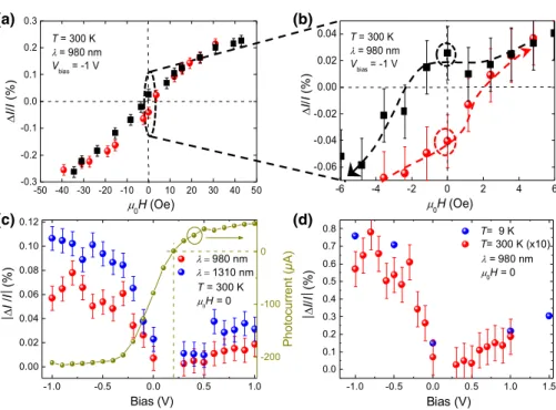
Figure 5(a) shows the evolution of the photocurrent helicity asymmetry, usually defined as $I/I = (Iσ+− Iσ−)/
[(Iσ++ Iσ−)/2], as a function of the applied magnetic field.
$I/I is measured with a laser wavelength λ of 980 nm under Vbias= −1 V and T = 300 K. It is obvious that
$I/I increases with the increase of the magnetic field. For µ0H = 43 Oe, $I/I reaches about 0.23%. As the
mag-netic field is swept from positive to negative values, $I/I changes its signs. Interestingly, at a zero applied magnetic field, the photocurrent helicity asymmetry is not equal to zero and seems to depend on the increasing or decreasing character of the sweep of the magnetic field. We have con-firmed this point by performing a sweep in the magnetic field with smaller steps around µ0H = 0 as shown in the
enlarged view [Fig.5(b)]. A helicity-dependent asymme-try of the photocurrent is thus evidenced without the need for any external magnetic field, contrary to previous works
(a) (b)
(c) (d)
FIG. 5. (a) Evolution of the asymmetry of the helicity-dependent photocurrent $I/I as a function of the applied magnetic field. Red circles and black squares correspond to increasing and decreasing magnetic fields, respectively. (b) Zoom of figure (a) in small magnetic field range. (c) |$I/I| measured as a function of the applied bias for two different excitation wavelengths (980 and 1310 nm) at RT without any applied magnetic field. The bias-dependent photocurrent with 980 nm excitation at RT is also shown. At a bias of 0.2 V (dashed line), the zero photocurrent indicates a flat band condition. (d) |$I/I| as a function of the applied bias measured at 9 and 300 K at zero magnetic field. The excitation wavelength is kept at 980 nm. For comparison with the low temperature measurements, the data measured at RT (shown as red circles) are multiplied by 10.
[28,45]. However, the dependence of $I/I as a function of µ0H does not follow the hysteresis cycle of the Co-Fe-B
injector measured by SQUID [Fig.3(b)]. Since the spin-filtering effect ($I/I) of the spin injector could be sensitive to the quality of the Co-Fe-B/MgO interface such as that in a spin-LED system [9], the magnetic field dependence of $I/I can reveal that the Co-Fe-B magnetization can be partially in-plane at the Co-Fe-B/MgO interface, which is very different from the PMA properties of the whole Co-Fe-B layer measured by SQUID [36,46].
Now we focus on the measurement of the photocurrent helicity asymmetry at zero field (µ0H = 0). Figure 5(c)
shows |$I/I| measured as a function of the applied bias for two different excitation wavelengths (980 and 1310 nm) at RT without any applied magnetic field. The clear varia-tion of |$I/I| as a funcvaria-tion of the applied bias is a strong indication that the observed helicity-dependent asymmetry cannot be attributed to the MCD effect [21]. The varia-tion mainly occurs for negative applied biases suggesting that the spin filtering of holes occurs. A similar observa-tion was also reported by Rinaldi et al. [28,45] on a device based on an electrode without PMA. Note that for excita-tion wavelengths λ = 980 nm and λ = 1310 nm, electrons and holes do not follow the same dynamics: electrons are
photo-generated in the & valley and are then very quickly scattered toward the L valley (approximately 200 fs [47]). On the contrary, the holes remain in the & valley where they have been photo-generated. Calculations based on density functional theory (DFT) indicate that the asym-metry (between spin up and down carriers) of the tunnel transmission coefficient through the MgO barrier is close to 100% in the & valley whereas it is only 35% in the L valley [28]. Thus, holes in the & valley will experience a very efficient spin filtering. However, the hole spin relax-ation time τsis very short, about 100 fs at RT [48]. On the other hand, despite a larger spin relaxation time expected for electrons (0.1–1 ns at RT [49]), the lower |$I/I| could be due to a weaker spin asymmetry of the tunnel transmis-sion coefficient through the MgO barrier in the L valley [28].
In order to estimate the maximum |$I/I| that we could reach, an analytic model has been developed (see Appendix) showing that |$I/I|maxscales with PS(1/λopt+
1/λR)λS for λS≪ λopt or λR, where PS is the photo-generated carrier spin polarization, λSis the spin diffusion length, λoptis the light absorption length, and λRis the car-rier recombination length. Taking into account a diffusion coefficient D for holes of about 0.0049 m2s−1[50] leads
to a hole spin diffusion length λS=√DτSof about 22 nm. Considering λopt∼ 400 nm at a wavelength of 980 nm [45],
an effective lifetime τR= λ2R/D of about 10 µs [51], and a photo-generated hole spin polarization PSof about 15% at 980 nm [52], one can expect a maximum of |$I/I| to be about 0.8% at RT. Therefore, the short hole spin relaxation time is a strong limitation that explains the weakness of the detected signal.
Let us now compare the evolution of |$I/I| as a func-tion of the applied bias when the excitafunc-tion wavelength is changed from 980 to 1310 nm: |$I/I| increases from about 0.06% to about 0.11% at Vbias= −1 V. This may be
par-tially due to an increased degree of optical spin orientation
Ps at 1310 nm as previously described by Rinaldi et al. [45] following the k·p calculation by Rioux and Sipe [52] (at this particular wavelength, a polarization of both elec-trons and holes of about 45% has indeed been predicted, instead of 15% at 980 nm). Moreover, longer spin relax-ation times for holes photo-generated at a lower energy are also expected to result in the larger |$I/I| values.
Finally, the temperature dependence of the helicity dependent photocurrent measured for an excitation wave-length of 980 nm is shown in Fig.5(d). When the tempera-ture decreases from 300 to 9 K, |$I/I| increases from about 0.06% to about 0.8%, i.e., by a factor of approximately 13. This could be linked to the increase of the carrier spin relaxation time (governed by carrier-phonon scattering) at low temperature that was reported for holes between 300 K (approximately 100 fs) [48] and 8 K (approxi-mately 100 ps) [53], and for electrons between 300 K (approximately 1 ns) [54] and 4 K (approximately 100 ns) [25].
Note that the use of an ultrathin Co-Fe-B layer ensures low light absorption in the metallic spin detector layer which is favorable for the realization of a photodetector. We can make a simple estimation of the light absorption with the formula P(t) = P0exp(−αt), where P0is the
inci-dent intensity and P(t) is the intensity transmitted through a layer of material with thickness t. The attenuation coeffi-cient is α. For a wavelength of 980 nm, the α of Fe is about 4.85 × 105 cm−1[55]. This leads the transmission of our
1.1-nm-thick magnetic electrode to be about 95%. How-ever, it should be noted that for the 40-nm-thick Fe/Tb layer as employed previously in Ref. [21], the transmission is much more attenuated, reaching only about 14%.
IV. CONCLUSIONS
To summarize, we investigate the growth of an ultrathin Co-Fe-B/MgO spin detector on Ge(001) sub-strates by using a combination of both MBE and sputtering methods. The epitaxial growth of MgO on Ge is observed with two different orientations, i.e., MgO[110](001)//Ge[100](001) corresponding to the major
growth direction and MgO[100](001)//Ge[100](001) cor-responding to the minor growth direction. The ultrathin Co-Fe-B/MgO spin detector is characterized by a strong perpendicular magnetic anisotropy in the range 10–300 K. The perpendicularly magnetized Co-Fe-B/MgO/Ge spin photodiodes gives rise to a photocurrent helicity asymme-try of about 0.9% at 10 K at 980 nm and of about 0.1% at RT at the telecommunication wavelength of 1310 nm without any applied magnetic field. Additional growth improvements are necessary in order to increase this asymmetry. In particular, the magnetic properties at the Co-Fe-B/MgO interface appear to be deteriorated com-pared to the magnetic properties of the Co-Fe-B layer itself. Our findings may pave the way for the development of a spin photocurrent detector on Ge(001) substrates for future optical transport of spin information.
ACKNOWLEDGMENTS
We thank Michel Hehn for help to develop the growth of ultrathin Co-Fe-B layer by sputtering. This work is supported by the joint French National Research Agency (ANR)-National Natural Science Foundation of China (NSFC) ENSEMBLE Project (Grants No. ANR-14-0028-01 and No. NNSFC 61411136001), SISTER Project (Grants No. ANR-11-IS10-0001 and No. NNSFC 61161130527) and by the French PIA project “Lorraine Université d’Excellence” (Grant No. ANR-15-IDEX-04-LUE). F.C. and P.R. acknowledge the Grant NEXT No. ANR-10-LABX-0037 in the framework of the Programme des Investissements d’Avenir. X.M. acknowledges Institut Universitaire de France. A.D acknowledges PhD fund-ing from Region Lorraine. Experiments were performed using equipment from the platform TUBE–Davm funded by FEDER (EU), ANR, the Region Lorraine, and Grand Nancy.
APPENDIX I. CALCULATION OF THE MAXIMUM OF PHOTOCURRENT HELICITY ASYMMETRY
We develop a simple analytic model to estimate the maximum of photocurrent helicity asymmetry in our mea-surement conditions. We have to discriminate between the hole and electron carrier photocurrent generated by optical pumping under the negative bias where the spin photocur-rent is maximum. Under these experimental conditions, the external electric field adds up to the built-in Schottky elec-tric field having the effect to drive the electrons out of the tunnel barrier interface region toward the “bulk” Ge and to drive the hole in the ferromagnetic contact through the tunnel barrier. We then mainly observe a hole photocur-rent. We demonstrate that the electric field has a dominant effect on the electron photocurrent and mostly no effect on the hole photocurrent. We then determine the equations of holes’ transport under pumping and the equations giv-ing the hole photocurrent. Our simplified equations will
slightly depart from the previous coupled electron-hole equations derived by Isella et al. [56] by the consideration of specific boundary conditions for a spin-polarized pho-tocurrent due to the presence of a contact resistance played by the tunnel barrier.
1. General transport equations for carriers involving the electric field effect
The general transport equations for pumped carriers’ density n(z) under a static electric field, E(z), are
J (z)
e = −D∇zn(z) + n(z)eµE(z) and (A1) dn(z)
dt = −∇zJ (z) − n(z)
τR + G(z), (A2)
where J (z) is the photocurrent, µ is the carrier mobility,
D = kTτp/e is the diffusion constant (τp is the character-istic collision time), and τRrepresents a certain relaxation time (spin-flip time in the present case). G(z) = G0e−
z λopt is the carrier generation per unit time by optical pump-ing rate which attenuates with an exponential absorption coefficient (inverse of the absorption length λopt). The first
equation expresses the dual contributions of the respective diffusive term, −D∇zn(z), and the drift term, n(z)eµE(z), on the current. The second equation expresses the charge conservation. Depending on the strength of the electric field with respect to a certain critical value, Ec, either the drift or diffusion contribution will be dominant. The development of the coupled equations gives a value of Ec
equaling Ec= D/µλR[57] where λR(=√DτR)is the cor-responding relaxation length (e.g., the spin diffusion length in the present case).
The examination of the present condition E ≪ D/µλR or E ≫ D/µλR with E ∼= e)/LD+ Ea where ) is the Schottky barrier height, LD is its depletion length (of the order of hundreds of 100 nm at low doping case), and Ea is the external electric field applied, leads to the conclu-sion that the electric field has almost no effect on the hole photocurrent (a very short spin-diffusion length of 22 nm leading to a strong diffusive current). On the contrary, the
E field is predominant for the electron photocurrent due to
its expected long spin-diffusion length at low doping of the order of 1 µm.
2. Transport equations for holes involving no electric-field effect
We consider now the detailed hole transport equation of density p(z) free of the presence of an electric field. One notes that p(z) is the profile of the optically pumped carrier density, thus the diffusive current J generated in Ge at zero bias can be described by the two equations concerning the
spatial distribution and dynamic equilibrium according to
J (z) e = −D∇zp(z) and (A3) dp(z) dt = −∇zJ (z) − p(z) τR + G(z). (A4)
For spin-polarized carriers, τR is the effective carrier recombination time involving the spin-flip term τs(1/τR= 1/τR0+ 1/τS)with τR0being the intrinsic unpolarized hole recombination time.
When dp(z)/dt = 0 in the steady-state regime, we get ∇zJ (z) = −p(z)
τR + G(z) . (A5)
By injecting equation(A3)into(A5)we obtain
D∂2p(z)
∂z2 =
p(z)
τR − G(z) . (A6)
One notes that DτR= λ2R, where λRis the carrier recombi-nation length, and in general λR̸= λopt.
By resolving the differential equation(A6)we get
p(z) = −G0/D
1/λ2
opt− 1/λ2R
e−(z/λopt)
+ $pe−(z/λR) (A7) where $p is a constant which can be determined by the boundary condition.
At the interface ferromagnet (FM)/semiconductor (SC) (z = 0), we get the current Jsfrom Eq.(A7):
Js|z=0 = −D∇zp(z = 0) = − G0/λopt 1/λ2 opt− 1/λ2R + $pD λR (A8) In fact, Jscan be also expressed as
Js|z=0= −VTsp(z = 0) = −VTs % −(G0/D) 1/λ2 opt− 1/λ2R + $ p & (A9) where VT
s is an effective “surface recombination velocity” (related to the tunneling transmission of the barrier).
Therefore, by the combination of Eqs.(A8)and (A9), we can deduce $pas follows:
$p = G0 1/λ2 opt− 1/λ2R "1/λopt+ VTs/D D/λR+ VTs # (A10) The measured photocurrent Iph can be expressed as
fol-lows: Iph= −Js= VTsp(z = 0) = VTs % −(G0/D) 1/λ2 opt− 1/λ2R + $ p & (A11) By injecting equation(A10)into(A11), we can get
Iph= V T s D ' −G0 1/λ2 opt− 1/λ2R+ G0 1/λ2 opt− 1/λ2R (VTs+ D/λopt) (VTs+ D/λR) ( = V T sG0 (1/λopt+ 1/λR) 1 (VTs + D/λR) (A12)
For the spin-polarized photocurrent, one can replace G0→ PSG0 (PS is the spin-polarization of carriers) and λR→ λS (λS is the spin diffusion length). The spin-polarized photocurrent IS phcan be expressed as IS ph= PSVTsG0 (1/λopt+ 1/λS) 1 (VTs + D/λS) (A13) The spin-polarization of the photocurrent is deter-mined by the ratio between IS
ph and Iph, and can be
expressed as P(ph) = I S ph Iph = PS "1/λopt+ 1/λR 1/λopt+ 1/λS # "VT s + D/λR VT s + D/λS # (A14) For the measured photocurrent helicity asymmetry in our paper, which can be further examined by the spin-dependent filtering of the FM spin detector as follows: $I I =P(ph) % VT↑s − VT↓s VT↑s + VT↓s & (A15) where VT↑s and VT↓s are surface recombination velocities related to the spin-up and spin-down carriers, respectively. Thus, the maximum of the photocurrent helicity asymme-try can be assumed to be ($I/I)max= P(ph)when (VT↑s − VT↓s )/(VT↑s + VT↓s )= 1.
Generally, λS ≪ λRor λopt, so Eq.(A15)can be
simpli-fied as " $I I # max= P (ph) = PS" 1 λopt + 1 λR # λS"V T s + D/λR VT s + D/λS # (A16) (1) In the limit condition of zero surface recombina-tion velocity (VT
s = 0), most of the photogenerated carriers are blocked by the barrier and recombined in the interface localized states: " $I I # max= P (ph) = PS" 1 λopt + 1 λR #λ2 S λR (A17)
(2) In the limit condition of a large surface velocity (large transmission coefficient), which corresponds to our experimental conditions, " $I I # max= P (ph) = PS" 1 λopt + 1 λR # λS (A18)
3. Transport equations for electrons involving the electric field effect
The transport equations in the case of a dominant elec-tric field (case of electrons) are
J (z)
e =n(z)eµE(z) and (A19)
dn(z)
dt = −∇zJ (z) − n(z)
τR + G(z) = 0. (A20)
This leads to the resolution of the equation for n(z) of the form n(z) − n(z = 0) =G0 µE 1 1/λopt− 1/λE(e −(z/λopt) − e−(z/λE)),
with λE= (eE/m)τpτS. The boundary condition at the interface with the tunnel barrier leads to n(z = 0) = 0 in that situation of an opposite current sign between electrons escaping toward the ferromagnetic contact and drift current toward the bulk Ge. The solution of the transport equation then is n(z) = G0 µE 1 1/λopt− 1/λE(e −(z/λopt) − e−(z/λE)).
[1] S. A. Wolf, D. D. Awschalom, R. A. Buhrman, J. M. Daughton, S. von Molnár, M. L. Roukes, A. Y. Chtchelka-nova, and D. M. Treger, Spintronics: A spin-based electron-ics vision for the future,Science 294, 1488 (2001).
[2] D. Awshalom and M. E. Flatte, Challenge for semiconduc-tor spintronics,Nat. Phys. 3, 153 (2007).
[3] R. Jansen, Silicon spintronics,Nat. Mater. 11, 400 (2012).
[4] Y. Lu, J. Li, and I. Appelbaum, Spin-Polarized Transient Electron Trapping in Phosphorus-Doped Silicon, Phys. Rev. Lett. 106, 217202 (2011).
[5] Y. Zhou, W. Han, L. T. Chang, F. X. Xiu, M. S. Wang, M. Oehme, I. A. Fischer, J. Schulze, R. K. Kawakami, and K. L. Wang, Electrical spin injection and transport in germanium,Phys. Rev. B 84, 125323 (2011).
[6] S. Liang, H. Yang, P. Renucci, B. Tao, P. Laczkowski, S. Mc-Murtry, G. Wang, X. Marie, J.-M. George, S. Petit-Watelot, A. Djeffal, S. Mangin, H. Jaffrès, and Y. Lu, Elec-trical spin injection and detection in molybdenum disulfide multilayer channel,Nat. Commun. 8, 14947 (2017).
[7] A. Fert and H. Jaffrès, Conditions for efficient spin injec-tion from a ferromagnetic metal into a semiconductor,Phys. Rev. B 64, 184420 (2001).
[8] Y. Lu, V. G. Truong, P. Renucci, M. Tran, H. Jaffrès, C. Der-anlot, J.-M. George, A. Lemaître, Y. Zheng, D. Demaille, P.-H. Binh, T. Amand, and X. Marie, MgO thickness depen-dence of spin injection efficiency in spin-light emitting diodes,Appl. Phys. Lett. 93, 152102 (2008).
[9] P. Barate, S. Liang, T. T. Zhang, J. Frougier, M. Vidal, P. Renucci, X. Devaux, B. Xu, H. Jaffrès, J. M. George, X. Marie, M. Hehn, S. Mangin, Y. Zheng, T. Amand, B. Tao, X. F. Han, Z. Wang, and Y. Lu, Electrical spin injection into InGaAs/GaAs quantum wells: A comparison between MgO tunnel barriers grown by sputtering and molecu-lar beam epitaxy methods,Appl. Phys. Lett. 105, 012404 (2014).
[10] R. Fiederling, M. Keim, G. Reuscher, W. Ossau, G. Schmidt, A. Waag, and L. W. Molenkamp, Injection and detection of a spin-polarized current in a light-emitting diode,Nature 402, 787 (1999).
[11] Y. Ohno, D. K. Young, B. Beschoten, F. Matsukura, H. Ohno, and D. D. Awschalom, Electrical spin injection in a ferromagnetic semiconductor heterostructure, Nature 402, 790 (1999).
[12] V. G. Truong, P.-H. Binh, P. Renucci, M. Tran, Y. Lu, H. Jaffrès, J.-M. George, C. Deranlot, A. Lemaître, T. Amand, and X. Marie, High speed pulsed electrical spin injection in spin-light emitting diode,Appl. Phys. Lett. 94, 141109 (2009).
[13] P. Barate, S. H. Liang, T. T. Zhang, J. Frougier, B. Xu, P. Schieffer, M. Vidal, H. Jaffrès, B. Lépine, S. Tricot, F. Cadiz, T. Garandel, J. M. George, T. Amand, X. Devaux, M. Hehn, S. Mangin, B. Tao, X. F. Han, Z. G. Wang, X. Marie, Y. Lu, and P. Renucci, Bias Dependence of the Elec-trical Spin Injection into GaAs from CoFeB/MgO Injectors with Different MgO Growth Processes,Phys. Rev. Appl. 8, 054027 (2017).
[14] S. H. Liang, T. T. Zhang, P. Barate, J. Frougier, M. Vidal, P. Renucci, B. Xu, H. Jaffrès, J. M. George, X. Devaux, M. Hehn, X. Marie, S. Mangin, H. X. Yang, A. Hallal, M. Chshiev, T. Amand, H. F. Liu, D. P. Liu, X. F. Han, Z. G. Wang, and Y. Lu, Large and robust electrical spin injec-tion into GaAs at zero magnetic field using an ultrathin CoFeB/MgO injector,Phys. Rev. B 90, 085310 (2014).
[15] J. Y. Chen, C. Y. Ho, M. L. Lu, L. J. Chu, K. C. Chen, S. W. Chu, W. Chen, C. Y. Mou, and Y. F. Chen, Efficient spin-light emitting diodes based on InGaN/GaN quantum disks
at room temperature: A new self-polarized paradigm,Nano Lett. 14, 3130 (2014).
[16] J. Y. Chen, T. M. Wong, C. W. Chang, C. Y. Dong, and Y. F. Chen, Spin-polarized spin-nanolasers,Nat. Nanotechnol.
9, 845 (2014).
[17] A. Bhattacharya, M. Z. Baten, I. Iorsh, T. Frost, A. Kavokin, and P. Bhattacharya, Room-Temperature Spin Polariton Diode Laser,Phys. Rev. Lett. 119, 067701 (2017).
[18] https://patents.google.com/patent/WO2011141304A2/ru:
Resonant diode having spin polarization for optoelectronic conversion.
[19] A. Hirohata, Y. B. Xu, C. M. Guertler, and J. A. C. Bland, Spin-dependent electron transport at the ferro-magnet/semiconductor interface,J. Appl. Phys. 85, 5804 (1999).
[20] T. Taniyama, G. Wastlbauer, A. Ionescu, M. Tselepi, and J. A. C. Bland, Spin-selective transport through Fe/AlOx/GaAs (100) interfaces under optical spin orienta-tion,Phys. Rev. B 68, 134430 (2003).
[21] S. HÓ˘gvel, N. C. Gerhardt, M. R. Hofmann, F. Y. Lo, D. Reuter, A. D. Wieck, E. Schuster, W. Keune, H. Wende, O. Petracic, and K. Westerholt, Electrical detection of photoin-duced spins both at room temperature and in remanence,
Appl. Phys. Lett. 92, 242102 (2008).
[22] R. C. Roca, N. Nishizawa, K. Nishibayashi, and H. Munekata, Investigation of helicity-dependent photocurrent at room temperature from a Fe/x-AlOx/p-GaAs Schottky junction with oblique surface illumination, Jpn. J. Appl. Phys. 56, 04CN05 (2017).
[23] L. Zhu, W. Huang, P. Renucci, X. Marie, Y. Liu, Y. Li, Q. Wu, Y. Zhang, B. Xu, Y. Lu, and Y. Chen, Angular Dependence of the Spin Photocurrent in a CoFeB/MgO/n-i-p GaAs Quantum Well Structure, Phys. Rev. Appl. 8, 064022 (2017).
[24] I. Zutic, J. Fabian, and S. Das Sarma, Spintronics: funda-mentals and applications,Rev. Mod. Phys. 76, 323 (2004).
[25] A. Giorgioni, E. Vitiello, E. Grilli, M. Guzzi, and F. Pezzoli, Valley-dependent spin polarization and long-lived elec-tron spins in germanium, Appl. Phys. Lett. 105, 152404 (2014).
[26] F. Rortais, C. Vergnaud, A. Marty, L. Vila, J. P. Attané, J. Widiez, C. Zucchetti, F. Bottegoni, H. Jaffrès, J. M. George, and M. Jamet, Non-local electrical spin injection and detec-tion in germanium at room temperature,Appl. Phys. Lett.
111, 182401 (2017).
[27] C. Rinaldi, M. Cantoni, D. Petti, and R. Bertacco, Epitax-ial Fe/MgO/Ge spin-photodiodes for integrated detection of light helicity at room temperature,J. Appl. Phys. 111, 07C312 (2012).
[28] C. Rinaldi, M. Cantoni, D. Petti, A. Sottocorno, M. Leone, N. M. Caffrey, S. Sanvito, and R. Bertacco, Ge-based spin-photodiodes for room temperature integrated detection of photo helicity,Adv. Mater. 24, 3037 (2012).
[29] F. Meier and B. P. Zakharchenya, Optical Orientation (North-Holland, Amsterdam, The Netherlands, 1984). [30] P. Renucci, V. G. Truong, H. Jaffrès, L. Lombez, P. H. Binh,
T. Amand, J. M. George, and X. Marie, Spin-polarized electroluminescence and spin-dependent photocurrent in hybrid semiconductor/ferromagnetic heterostructures: an asymmetric problem,Phys. Rev. B 82, 195317 (2010).
[31] R. Farshchi, M. Ramsteiner, J. Herfort, A. Tahraoui, and H. T. Grahn, Optical communication of spin information between light emitting diodes,Appl. Phys. Lett. 98, 162508 (2011).
[32] Pavel Potapov,www.temdm.com.
[33] S. Sun, Y. Sun, Z. Liu, D. I. Lee, S. Peterson, and P. Pianetta, Surface termination and roughness of Ge (100) cleaned by HF and HCl solutions,Appl. Phys. Lett. 88, 021903 (2006).
[34] D. Petti, M. Cantoni, C. Rinaldi, S. Brivio, R. Bertacco, J. Gazquez, and M. Varela, Sharp Fe/MgO/Ge (001) epitaxial heterostructure for tunneling junctions,J. Appl. Phys. 109, 084909 (2011).
[35] J. Narayan and B. C. Larson, Domain epitaxy: A uni-fied paradigm for thin film growth,J. Appl. Phys. 93, 278 (2003).
[36] B. Tao, P. Barate, X. Devaux, P. Renucci, J. Frougier, A. Djeffal, S. Liang, B. Xu, M. Hehn, H. Jaffrès, J.-M. George, X. Marie, S. Mangin, X. F. Han, Z. G. Wang, and Y. Lu, Atomic-scale understanding of high thermal stability of the Mo/CoFeB/MgO spin injector for spin-injection in remanence,Nanoscale 10, 10213 (2018).
[37] Y. Lu, B. Lépine, G. Jézéquel, S. Ababou, M. Anlot, J. Lambert, A. Renard, M. Mullet, C. Deranlot, H. Jaf-frès, F. Petroff, and J.-M. George, Depth analysis of boron diffusion in MgO/CoFeB bilayer by x-ray photoelectron spectroscopy,J. Appl. Phys. 108, 043703 (2010).
[38] Z. Wang, M. Saito, K. P. McKenna, S. Fukami, H. Sato, S. Ikeda, H. Ohno, and Y. Ikuhara, Atomic-scale structure and local chemistry of CoFeB/MgO magnetic tunnel junctions,
Nano Lett. 16, 1530 (2016).
[39] S. Ikeda, K. Miura, H. Yamamoto, K. Mizunuma, H. D. Gan, M. Endo, S. Kanai, J. Hayakawa, F. Matsukura, and H. Ohno, A perpendicular-anisotropy CoFeB/MgO magnetic tunnel junction,Nat. Mater. 9, 721 (2010).
[40] J. Hauschild, H. Fritzsche, S. Bonn, and Y. Liu, Deter-mination of the temperature dependence of the coerciv-ity in Fe/Cr (110) multilayers, Appl. Phys. A 74, S1541 (2002).
[41] A. Raghunathan, Y. Melikhov, J. E. Snyder, and D. C. Jile, Theoretical model of temperature dependence of hysteresis based on mean field theory,IEEE Trans. Magn. 46, 1507 (2010).
[42] M. Yamanouchi, A. Jander, P. Dhagat, S. Ikeda, F. Mat-sukura, and H. Ohno, Domain structure in CoFeB thin films with perpendicular magnetic anisotropy,IEEE Magn. Lett.
2, 3000304 (2011).
[43] K.-R. Jeon, B.-C. Min, H.-S. Lee, I.-J. Shin, C.-Y. Park, and S.-C. Shin, Single crystalline CoFe/MgO tunnel contact on nondegenerate Ge with a proper resistance-area product for efficient spin injection and detection,Appl. Phys. Lett. 97, 022105 (2010).
[44] Y. Zhou, W. Han, Y. Wang, F. Xiu, J. Zou, R. K. Kawakami, and K. L. Wang, Investigating the orgin of Fermi level
pinning in Ge Schottky junctions using epitaxially grown ultrathin MgO films,Appl. Phys. Lett. 96, 102103 (2010).
[45] C. Rinaldi, M. Cantoni, M. Marangoni, C. Manzoni, G. Cerullo, and R. Bertacco, Wide-range optical spin orien-tation in Ge from near-infrared to visible light,Phys. Rev. B 90, 161304(R) (2014).
[46] B. S. Tao, P. Barate, J. Frougier, P. Renucci, B. Xu, A. Djef-fal, H. Jaffrès, J.-M. George, X. Marie, S. Petit-Watelot, S. Mangin, X. F. Han, Z. G. Wang, and Y. Lu, Electrical spin injection into GaAs based light emitting diodes using perpendicular magnetic tunnel junction-type spin injector,
Appl. Phys. Lett. 108, 152404 (2016).
[47] E. J. Loren, J. Rioux, C. Lange, J. E. Sipe, H. M. van Driel, and A. L. Smirl, Hole spin relaxation and intervalley electron scattering in germanium,Phys. Rev. B 84, 214307 (2011).
[48] E. J. Loren, B. A. Ruzicka, L. K. Werake, H. Zhao, H. M. Van Driel, and A. L. Smirl, Optical injection and detection of ballistic pure spin currents in Ge,Appl. Phys. Lett. 95, 092107 (2009).
[49] S. Patibandla, G. M. Atkinson, S. Bandyopadhyay, and G. C. Tepper, Competing D’yakonov-Perel’ and Elliott-Yafet spin relaxation in germanium,Physica E 42, 1721 (2010).
[50] O. A. Golikova, B. Ya Moizhez, and L. S. Stilbans, Hole mobility of germanium as a function of concentration and temperature, Sov. Phys. Solid State 3, 2259 (1962). [51] E. Gaubas and J. Vanhellemont, Dependence of carrier
life-time in germanium on resistivity and carrier injection level,
Appl. Phys. Lett. 89, 142106 (2006).
[52] J. Rioux and J. E. Sipe, Optical injection and control in ger-manium: Thirty-band k · p theory,Phys. Rev. B 81, 155215 (2010).
[53] C. Hautmann, B. Surrer, and M. Betz, Ultrafast optical ori-entation and coherent Larmor precession and electron and hole spins in bulk germanium,Phys. Rev. B 83, 161203(R) (2011).
[54] A. Jain, J.-C. Rojas-Sanchez, M. Cubukcu, J. Peiro, J. C. Le Breton, E. Prestat, C. Vergnaud, L. Louahadj, C. Portemont, C. Ducruet, V. Baltz, A. Barski, P. Bayle-Guillemaud, L. Vila, J.-P. Attané, E. Augendre, G. Desfonds, S. Gam-barelli, H. Jaffrès, J.-M. George, and M. Jamet, Crossover from Spin Accumulation into Interface States to Spin Injec-tion in the Germanium ConducInjec-tion Band,Phys. Rev. Lett.
109, 106603 (2012).
[55] P. B. Johnson and R. W. Christy, Optical constants of tran-sition metals: Ti, V, Cr, Mn, Fe, Co, Ni and Pd,Phys. Rev. B 9, 5056 (1974).
[56] G. Isella, F. Bottegoni, A. Ferrari, M. Finazzi, and F. Cic-cacci, Photo energy dependence of photo-induced inverse spin-hall effect in Pt/GaAs and Pt/Ge,Appl. Phys. Lett. 106, 232402 (2015).
[57] Z. G. Yu and M. E. Flatté, Spin diffusion and injection in semiconductor structures: Electric field effects,Phys. Rev. B 66, 235302 (2002).