HAL Id: hal-00909676
https://hal.archives-ouvertes.fr/hal-00909676
Submitted on 9 Mar 2018
HAL is a multi-disciplinary open access
archive for the deposit and dissemination of
sci-entific research documents, whether they are
pub-lished or not. The documents may come from
teaching and research institutions in France or
abroad, or from public or private research centers.
L’archive ouverte pluridisciplinaire HAL, est
destinée au dépôt et à la diffusion de documents
scientifiques de niveau recherche, publiés ou non,
émanant des établissements d’enseignement et de
recherche français ou étrangers, des laboratoires
publics ou privés.
Examination of femtosecond laser matter interaction in
multipulse regime for surface nanopatterning of vitreous
substrates
Nadezda Varkentina, Thierry Cardinal, Fabien Moroté, Patrick Mounaix,
Pascal André, Yannick Deshayes, Lionel Canioni
To cite this version:
Nadezda Varkentina, Thierry Cardinal, Fabien Moroté, Patrick Mounaix, Pascal André, et al..
Ex-amination of femtosecond laser matter interaction in multipulse regime for surface nanopatterning
of vitreous substrates. Optics Express, Optical Society of America - OSA Publishing, 2013, 21 (24),
pp.29090-29100. �10.1364/OE.21.029090�. �hal-00909676�
Examination of femtosecond laser
matter interaction in multipulse regime
for surface nanopatterning of vitreous
substrates
Nadezda Varkentina,1,∗Thierry Cardinal,2Fabien Morot´e,1Patrick Mounaix,1Pascal Andr´e,3Yannick Deshayes,1,3and Lionel Canioni1
1Univ. Bordeaux, LOMA, UMR 5798, F-33400 Talence, France 2Univ. Bordeaux, ICMCB, UPR 9048, F-33400 Pessac, France 3Univ. Bordeaux, IMS, UMR 5218, F-33400 Talence, France
*nadezda.varkentina@u-bordeaux1.fr
Abstract: The paper presents our results on laser micro- and nanostruc-turing of sodium aluminosilicate glass for the permanent storage purposes and photonics applications. Surface structuring is realized by fs laser irradiation followed by the subsequent etching in a potassium hydroxide (10M@80◦C) for 1 to 10 minutes. As the energy deposited is lower than the damage and/or ablation threshold, the chemical etching permits to produce small craters in the laser modified region. The laser parameters dependent interaction regimes are revealed by microscopic analysis (SEM and AFM). The influence of etching time on craters formation is investigated under different incident energies, number of pulses and polarization states.
© 2013 Optical Society of America
OCIS codes: (320.2250) Femtosecond phenomena; (160.2750) Materials: Glass and other amorphous materials; (230.4000) Optical devices: Microstructure fabrication; (320.7130) Ul-trafast optics : UlUl-trafast processes in condensed matter, including semiconductors.
References and links
1. A. P. Joglekar, H. Liu, G. J. Spooner, E. Meyh¨ofer, G. Mourou, and A. J. Hunt, “A study of the deterministic character of optical damage by femtosecond laser pulses and applications to nanomachining,” Appl. Phys. B 77, 25–30 (2003).
2. B.-B. Xu, Y.-L. Zhang, H. Xia, W.-F. Dong, H. Ding, and H.-B Sun, “Fabrication and multifunction integration of microfluidic chips by femtosecond laser direct writing,” Lab chip 13, 1677–1690 (2013).
3. D. B¨auerle, “Laser chemical processing: an overview to the 30th anniversary,” Appl. Phys. A 101(2) 447–459 (2010).
4. S. H. Chung and E. Mazur, “Surgical applications of femtosecond lasers,” J. of Biophoton. 2(10) 557–1381 (2009).
5. M. Ams, G. D. Marshall, P. Dekker, M. Dubov, V. K. Mezentsev, I. Bennion, and M. J. Withford, “Investigation of ultrafast laser-photonic material interactions: Challenges for directly written glass photonics,” IEEE J. Quantum Electron. 14(5) 1370–1381 (2008).
6. D. Ghezzi, R. M. Vazquez, R. Osellame, F. Valtorta, A. Pedrocchi, G. D. Valle, R. Ramponi, G. Ferrigno, and G. Cerullo, “Femtosecond laser microfabrication of an integrated device for optical release and sensing of bioactive compounds,” Sensors 8(10) 6595–6604 (2008).
7. P. Zijlstra, J. W. M. Chon, and M. Gu, “Five-dimensional optical recording mediated by surface plasmons in gold nanorods,” Nature (London) 459, 410–413 (2009).
8. A. Royon, K. Bourhis, M. Bellec, G. Papon, B. Bousquet, Y. Deshayes, T. Cardinal, and L. Canioni, “Silver Clusters Embedded in Glass as a Perennial High Capacity Optical Recording Medium,” Advanc. Mat. 2,(46) 5282–5286 (2010).
#193141 - $15.00 USD Received 4 Jul 2013; revised 23 Oct 2013; accepted 26 Oct 2013; published 18 Nov 2013
9. M. Shiozawa, T. Watanabe, E. Tatsu, M. Umeda, T. Mine, Y. Shimotsuma, M. Sakakura, M. Nakabayashi, K. Miura, and K. Watanabe, “Simultaneous multi-bit recording in fused silica for permanent storage,” presented at the International Symposuim on Optical Memory 2012, Tokyo, Japan, Sep. 30–Oct. 4, 2012.
10. D. Du, X. Liu, and G. Mourou, “Reduction of multi-photon ionization in dielectrics due to collisions,” Appl. Phys. B 63, 617–621 (1996).
11. H. Varel, D. Ashkenasi, A. Rosenfeld, R. Herrmann, F. Noack, and E. Campbell, “Laser- induced damage in SiO2
and CaF with picosecond and femtosecond laser pulses with picosecond and femtosecond laser pulses,” Appl. Phys. A 62, 293–294 (1996).
12. A-C. Tien, S. Backus, H. Kapteyn, M. Murnane, and G. Mourou, “Short-pulse laser damage in transparent mate-rials as a function of pulse duration,” Phys. Rev. Lett. 8(19) 3883–3886 (1999).
13. M. Li, S. Menon, J. P. Nibarger, and G. N. Gibson, “Ultrafast electron dynamics in femtosecond optical break-down of dielectrics,” Phys. Rev. Lett. 82(11) 2394–2397 (1999).
14. S. Xu, J. Qiu, T. Jia, C. Li, H. Sun, and Z. Xu, “Femtosecond laser ablation of crystals SiO2and YAG,” Opt.
Commun. 274, 163–166 (2007).
15. N. Sanner, O. Ut´eza, B. Bussi`ere, G. Coustillier, A. Leray, T. Itina, and M. Sentis, “Measurement of femtosecond laser-induced damage and ablation thresholds in dielectrics,” Appl. Phys. A 94, 889–897 (2009).
16. N. Varkentina, N. Sanner, M. Lebugle, O. Ut´eza, and M. Sentis, “Absorption of a single 500 fs laser pulse at the surface of fused silica: energy balance and ablation efficiency,” J. Appl. Phys. 14, 173105 (2013).
17. D. Puerto, W. Gawelda, J. Siegel, J. Bonse, G. Bachelier, and J. Solis, “Transient reflectivity and transmission changes during plasma formotion and ablation in fused silica induced by femtosecond laser pulses,” Appl. Phys. A 92, 803–808 (2008).
18. D. Puerto, J. Siegel, W. Gawelda, M. Galvan-Sosa, L. Ehrentraut, J. Bonse, and J. Solis, “Dynamics of plasma formation, relaxation, and topography modification induced by femtosecond laser pulses in crystalline and amor-phous dielectrics,” J. Opt. Soc. Am. B 27,(5) 1065–1076 (2010).
19. I. H. Chowdhury and X. Xu, “Ultrafast double-pulse ablation of fused silica,” Appl. Phys. Lett. 86, 151110– 151112 (2005).
20. I. H. Chowdhury, X. Xu, and A. M. Weiner, “Ultrafast two-color ablation of fused silica,” Appl. Phys. A 83, 49–52 (2006).
21. Y. Bellouard, A. Said, M. Dugan, and P. Bado, “Fabrication of high-aspect ratio, micro-fluidic channels and tunnels using femtosecond laser pulses and chemical etching,” Opt. Express 12(10), 2120–2129 (2004),
http://www.opticsinfobase.org/oe/abstract.cfm?URI=oe-12-10-2120.
22. A. A. Said, M. Dugan, P. Bado, Y. Bellouard, A. Scott, and J. R. Mabes, Jr., “Manufacturing by laser direct-write of three-dimensional devices containing optical and microfluidic networks,” in Photon Processing in Microelec-tronics and Photonics III,Proc. SPIE 5339 194 (2004).
23. J. Bonse, J. Kr¨uger, S. H¨ohm, and A. Rosenfeld, “Femtosecond laser-induced periodic surface structures,” J. Las. Appl. 24, 042006–042013 (2012).
24. R. Buividas, L. Rosa, R. Sliupas, T. Kudrius, G. Slekys, V. Datsyuk, and S. Juodkazis, “Mechanism of fine ripple formation on surfaces of (semi)transparent materials via a half-wavelength cavity feedback,” Nanotech. 22, 055304 (2011).
25. F. Costache, M. Henyk, and J. Reif, “Surface patterning on insulators upon femtosecond laser ablation,” Appl. Surf. Sci. 208-209, 486–491 (2003).
26. F. Liang, R. Vall´ee, and S. L. Chin, “Mechanism of nanograting formation on the surface of fused silica,” Opt. Express 20(4) 4389–4396 (2012),http://www.opticsexpress.org/abstract.cfm?URI=OPEX-20-4-4389. 27. F. Garrelie, J. P. Colombier, F. Pigeon, S. Tonchev, N. Faure, M. Bounhalli, S. Reynaud, and O. Parriaux,
“Evi-dence of surface plasmon resonance in ultrafast laser-induced ripples,” Opt. Express 19(10) 9035–9043 (2011),
http://www.opticsexpress.org/abstract.cfm?URI=OPEX-19-10-9035.
28. R. Wagner, J. Gottmann, A. Horn, and E. W. Kreutz, “Subwavelength ripple formation induced by tightly focused femtosecond laser radiation,” Appl. Surf. Sci. 252, 8576–8579 (2006).
29. L. Sudrie, M. Franco, B. Prade, and A. Mysyrowicz, “Study of damage in fused silica induced by ultra-short IR laser pulses,” Opt. Com. 191, 333–339 (2001).
30. Y. Shimotsuma, P. G. Kazansky, J. Qiu, and K. Hirao, “Self-organized nanogratings in glass irradiated by ultra-short light pulses,” Phys. Rev. Lett. 91, 247405 (2003).
31. N. Glezer and E. Mazur, “Ultrafast-laser driven micro-explosions in transparent materials,” Appl. Phys. Lett. 71, 882–884 (1997).
32. J. M. Fern´andez-Pradas, D. Comas, J. L. Morenza, and P. Serra, “Irradiation of glass with infrared femtosecond laser pulses,” Appl. Phys. A 112, 203–207 (2013).
33. Y. Li, W. Watanabe, K. Yamada, T. Shinagawa, K. Itoh, J. Nishii, and Y. Jiang, “Holographic fabrication of multiple layers of grating inside sodalime glass with femtosecond laser pulses,” Appl. Phys. Lett. 80(9) 1508– 1510 (2002).
34. J. B. Lonzaga, S. M. Avanesyan, S. C. Langford, and J. T. Dickinson, “Color center formation in soda-lime glass with femtosecond laser pulses,” J. Appl. Phys. 94)(7) 4332–4340 (2003).
with aqueous solution of KOH,” in Proceedings of the sixth international conference on photo-excited processes and applications (6-ICPEPA),Appl. Surf. Sci. 255(24) 9758–9760 (2009).
36. A. Rosenfeld, M. Lorenz, R. Stoian, and D. Ashkenasi, “Ultrashort-laser pulse damage threshold of transparent materials and the role of incubation,” Appl. Phys. A 69, S373–S376 (1999).
37. C. Hnatovsky, R. S. Taylor, E. Simova, P. P. Rajeev, D. M. Rayner, V. R. Bhardwaj, and P. B. Corkum, “Fabrica-tion of microchannels in glass using focused femtosecond laser radia“Fabrica-tion and selective chemical etching,” Appl. Phys. A 84(1-2) 47–56 (2006).
38. S. Kiyama, S. Matsuo, S. Hashimoto, and Y. Morihira, “Examination of etching agent and etching mechanism on femotosecond laser microfabrication of channels inside vitreous silica substrates,” J. Phys. Chem. C 113(27) 11560–11566 (2009).
39. F. Madani-Grasset and Y. Bellouard, “Femtosecond laser micromachining of fused silica molds,” Opt. Express 18(21) 21826–21840 (2010),http://www.opticsexpress.org/abstract.cfm?URI=OPEX-18-21-21826.
40. L. Bressel, D. de Ligny, C. Sonneville, V. Martinez, V. Mizeikis, R. Buividas, and S. Juodkazis “Femtosecond laser induced density changes in GeO2and SiO2glasses: fictive temperature effect,” Opt. Mat. Express 1,(4)
605–613 (2011),http://www.opticsinfobase.org/ome/abstract.cfm?URI=ome-1-4-605.
41. A. Ben-Yakar, A. Harkin, J. Ashmore, R. L. Byer, and H. A. Stone, “Thermal and fluid processes of a thin melt zone during femtosecond laser ablation of glass: the formation of rims by single laser pulses,” J. Phys. D: Appl. Phys. 40, 1447–1459 (2007).
42. N. Varkentina, O. Ut´eza, N. Sanner, B. Chimier, M. Sentis, and T. Itina, “Absorption of femtosecond laser pulse in fused silica: experiments and modelling,” in International Conference on Laser Applications in Microelectronic and Optoelectronic Manufacturing (LAMOM) XVI,B. Gu and G. Hennig and X. Xu and H. Niino, eds., Proc. SPIE 7920, 792003 (2011).
43. D. Grojo, M. Gertsvolf, S. Lei, T. Barillot, D. M. Rayner, and P. B. Corkum, “Exciton-seeded multiphoton ionization in bulk SiO2,” Phys. Rev. B 81, 212301 (2010).
44. K. Bourhis, A. Royon, M. Bellec, J. Choi, A. Fargues, M. Treguer, J.-J. Videau, D. Talaga, M. Richardson, T. Cardinal, and L. Canioni, “Femtosecond laser structuring and optical properties of a silver and zinc phosphate glass,” J. Non-Cryst. Solids 356(44-49) 2658–2665 (2010).
45. A. N. Trukhin, J. Teteris, A. Fedotov, D. L. Griscom, and G. Buscarino, “Photosensitivity of SiO2–Al and SiO2–
Na glasses under ArF (193 nm) laser,” J. Non-cristal. Solids 355, 1066–1074 (2009).
46. E. A. Vanina, M. A. Chibisova, and S. M. Sokolova, “Effect of radiation bleaching in sodium-silicate glasses,” Glass and Ceramics 63(11-12) 366–367 (2006).
47. K. Kadono, N. Itakura, T. Akai, M. Yamashita, and T. Yazawa, “The effet of additive ions on the optical density and stability of the color centers induced by X-Ray irradiation in soda lime silicate glass,” Nuclear Instrum. Method. in Phys. Research B 267, 2411–2415 (2009).
1. Introduction
Nowadays, the high intensity of femtosecond laser pulses allows an extremely high precision in terms of localization of the deposited energy and thus the minimal affected zone and the reinforced resolution during micro-machining process [1]. This particular feature is due to the highly nonlinear nature of the laser-matter interaction for wide bandgap materials and has in-teresting applications especially in photonics, medicine and in the technologies of information and telecommunications [2–6]. Recently, from the increasing necessity of data handling and conservation, a new research field has emerged: the application of ultra fast technologies for long-term information storage [7–9].
Up today numerous researches have adressed the mechanisms of femtosecond laser interaction with dielectrics, in particular, for single shot interaction. One of the widely studied parame-ters is the fluence threshold, which varies strongly depending on the definition even in similar experimental conditions (800 nm, fused silica, single shot regime) [10–14]. Sanner et al. [15] gives the precise definition of damage and ablation thresholds, which is material property de-pendent, technique dependent and diagnostic dependent. Thus the methodology of the thresh-old measurement should be defined precisely for each experiment. The distinction of the two thresholds is of the great importance due to the difference in absorption and subsequent final material modifications [16]. Various works have been done on the dynamics of the reflection and transmission change during the laser pulse and after the end of the energy deposition. This works have studied, described and analyzed the plasma excitation and relaxation. Puerto et
#193141 - $15.00 USD Received 4 Jul 2013; revised 23 Oct 2013; accepted 26 Oct 2013; published 18 Nov 2013
al. [17, 18] with time-resolved transmission measurements demonstrates two concentric rings: one corresponding to laser ablation and the second to the affected zone. Depending on matrix structure organization (crystalline or amorphous), it explains the difference of the final ablation craters caused by different viscosity of crystalline and amorphous dielectrics. Chowdhury et al. [19, 20] demonstrates enhanced absorption due to defect generation. In particular, the pre-cise knowledge of the deposited energy per unit volume allows defining the efficiency of the laser energy deposition and its redistribution after the end of the interaction [16]. The multishot material modifications, notably, in the bulk of transparent solids, are interesting for applications such as waveguiding, microfluidics and photonic structures [5, 21, 22]. Those modifications are usually associated with refractive index modification and void formation. Surface experiments of wide bandgap dielectric materials include the study of ripples or so-called nano-gratings formation [23–28]. Ripples formation emerges from the enhancement of the electric field on the surface of material. The period of coarse ripples, which is characteristic for all materials (metals, semiconductors, dielectrics), is close to the wavelength of laser irradiation and is con-sidered to be the produced by the interference of the incident and scattered standing wave. Nano-gratings or fine ripples are presumably result in the highly localized nanophotonic and incubation effects on the sites of defects formation [24–26, 28]. The period of fine ripples is dependent on the refractive index of material.
In bulk, there are three types of the material modifications. At low energy density (type 1 modification), the local refractive index change ∆n is isotropic [29]. At intermediate energy density (type 2 modification), ∆n is anisotropic due to the presence of nano-gratings [30]. At high energy density (type 3 modification), voids with a low index core and a high index shell are formed [31].
There are only a few studies on the effects of the femtosecond laser radiation on silicate glass [32–35] compared to fused silica glass. Whereas, it is the most common material in the glass industry. Ablation threshold was measured for soda lime silicate glass irradiated with a femtosecond laser (450 fs @ 1027 nm) [32]. Laser fluence threshold is 6.4 J/cm2for a single laser pulse and decreases with the number of incident pulses, saturating at 3.2 J/cm2for 10-1000 pulses due to accumulation [32,36]. The estimation of the interaction energy assumes 4 photons absorption for the non-linear material modification as compared to 8 photons absorption in fused silica.
Our paper is focused on the modification of sodium aluminosilicate glass under multipulse femtosecond laser irradiation for application on long-term data storage. Moreover, in this work we explore and introduce subthreshold surface modifications in multishot regime for high repe-tition rate femtosecond lasers. We present the successive steps of material surface modifications from chemical structure reorganization to strong ablation as a function of incident energy and number of pulses.
2. Experimental methods
2.1. Laser microstructuring test-bench
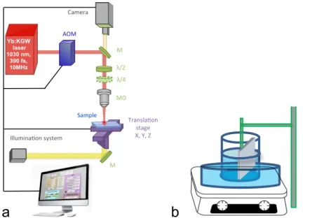
The experimental test-bench for surface nano-patterning: Fig. 1(a) consists of the laser system (Yb:KGW commercial laser Amplitude Systemes, t-pulse 200, 10 MHz) with pulse duration of 390 fs at operating wavelength 1030 nm. The collimated laser beam of ∼ 4.0 mm is fo-cused normally on the sample surface, using a high numerical aperture microscope objective (Mitutoyo Plan Apo NIR HR, N.A. = 0.7, 100x).
The beam diameter yields 2ω0= 2.3 µm measured via two photon absorption of a photodiode at 1/e2in the focal plane. CCD camera coupled to the white light source is handled for the laser beam positioning and diagnostics. The target displacement is assured by three x, y, z -motorized translation stages (XMS-50 stages, Micro-Contrˆole with minimal displacement step
Yb:KGW laser 1030 nm, 390 fs, 10MHz Camera AOM M Transla-on stage X, Y, Z MO M λ/2 λ/4 Sample Illumina-on system
!
a
b
Fig. 1. Experimental test-bench for laser surface micro-structuring (a) and chemical etching (b). M mirror; AOM Acoustooptic modulator; MO Microscope objective ; Camera -Visualization system.
of 10 nm and maximal displacement speed of 25 mm/s). The translation stages are operated by a home-made computer program using IGOR Pro (WaveMetrics) and XPS Motion Controller. The acousto-optic modulator serves for the precise adjustment of incident surface energy and number of pulses. All experiments are produced at ambient temperature and normal pressure. Samples consist of sodium aluminosilicate glass. The chemical composition of the glass is given in table 1.
Cationic chemical element Weight, %
Si 63.7 Al 16.4 Na 15.4 Ca 2.9 Mg 1.4 Fe 0.2 Sb 171 ppm Sn 174 ppm
Table 1. Elemental chemical concentration of cations in the sodium aluminosilicate glass samples measured by electron probe microanalyzer.
The glass investigated is a sodium aluminosilicate glass containing calcium and manganese with low concentration of iron and hundred of ppm of antimony and tin. The damage thresh-old is defined as a maximal energy not to cause visible material modifications measured with adapted illumination and magnification. It gives values between 21.7 to 18.9 nJ (for 102to 106 pulses) and 24.1 nJ (for 10 pulses) defined by optical microscopy technique. Laser threshold fluence estimated according to the following definition: F = 2E/πω2[15] gives 1 J/cm2for 102
#193141 - $15.00 USD Received 4 Jul 2013; revised 23 Oct 2013; accepted 26 Oct 2013; published 18 Nov 2013
pulses, 0.9 J/cm2for 106pulses and 1.2 J/cm2for 10 pulses. Surface topology measurements are performed with both high resolution SEM and Atomic Force Microscope (AFM Veeco Dimension 3000) to get exhaustive information about surface evolution depending on etching time. AFM tip measurement with a calibrated object is performed prior to the measurement of nanostructures on the surface of the target.
2.2. KOH etching experimental set-up
When the standard procedure of laser inscription is finished, the sample is cleaned in ultrasonic bath for 10 min in two separate solutions: the first, ethanol and, the second, acetone (both HPLC grade). Each time the specimen is rinsed with Ultrapure Millipore water (pH 5.5, resistivity > 18 MΩ cm) and dried. Then the target is wet etched in a highly concentrated potassium hydroxide (10M) at the temperature of 80◦C for 1, 2, 5 and 10 minutes (see Fig. 1(b)).
It is known, that for fused silica, HF wet etching is used as a common agent for microfluidic purposes in the surface or in the bulk [22, 37, 38]. Once the material properties are changed by the laser irradiation, one states higher sensitivity of the etching of modified zone compared to non-modified one. S. Kiyama et al. [38] has done an extensive study comparing the HF and KOH on silica. The maximal contrast between laser irradiated and non-irradiated zone equals to 200 for the KOH and 50 for the HF etching agents [38]. Etching of the material bulk concerns types 1 and 2 modifications. The polarisation dependent phenomena is demonstrated for both etchants. For the HF the dependence of etching on polarization state diminishes with incident energy increase. For the KOH this phenomena is not pronounced even at high incident laser energy. S. Kiyama et al. [38] assumes that the densification of fused silica is the reason of in-creased contrast for the HF etching. In silica, the possible explications of the different contrasts between two etching agents is relevant to the difference of chemical reactions. Acid solution is active in disruption of Si–O bonds, which explains etching of non-modified glass as well. Acid attacks strongly the regions with nanocracks and pressure increase in the laser-affected zone [21, 39]. It is thus sensitive to the pressure and mechanical material properties change. In the same time, the presence of increased number of Si–Si bonds [40] are highly vulnerable to basic aqueous solution. Regarding the KOH etching, the mechanisms are less understood. For silicate glass the mechanism of etching under laser exposure will be dependent on the glass composition and few studies have been carried out. Since the color centers formation and their concentration are depent on the glass composition, one can expect also different etching mech-anisms depending on the glass composition. The KOH etching contrast achieved in borosilicate Pyrex type glass is, for instance, 500 [35] compared to 200 for fused silica.
3. Results and discussion 3.1. Direct laser nano-patterning
The schematic representation of the laser induced modifications on the surface of sodium alu-minosilicate glass is given in Fig. 2. One distinguishes A, B, C, D, E zones. The A zone corre-sponds to no detectable modifications by implemented techniques such as optical microscopy, SEM and AFM. In the B zone no material modification are measurable after laser irradiation. Nevertheless, subthreshold modifications are present and revealed by KOH etching. In the C zone surface nano-hills are produced directly by femtosecond laser processing. The D zone is the zone with nano-gratings surface modification, where nano-gratings from single groove up to ripple material structure are fabricated. The E zone represents thermal ablation. The dotted lines summarises the figures of the whole article.
At high energy density, surface nanopatterning drives to the ablation of the central zone sur-rounded by a resolidified surface rim (depicted in Fig. 2 as thermal ablation) [41]. The craters are circular and non-sensitive to polarization state.
!"#$ %&' ()*+#,-').' /0 12 *+ '34'5067* 7' 89:' 89;' 89<' 898' 899' 89%' 89=' <9' %9' =9' !"#$ ;&' !"#$ %2' !"#$':' /3'>"7"26*' 13?"@A&B3)7' C02DE+*7E36?' )&)3F7D+0AD0+*7' /&)3FE"667'G?&1&#*' DE+*7E36?7' /&)3F#+&B)#7' HE*+1&6'&26&B3)' !"#$ =' !"#$ ;2'
A
B
C
D
A
B
C
D
E
E
Fig. 2. General sketch of the regimes of laser surface modifications for high repetition rate lasers and wet etching.
The decrease of the incident energy and/or number of incident pulses causes another phe-nomenon reported as nano-gratings (see Figs. 3 or 6). F. Liang, R. Vall´ee et al. [26] present a model based on the photonic effect to explain it. This ablation zone is first trigged by the defects created by the subsequent pulses due to the incubation process [36] in the direction per-pendicular to electric field (see Figs. 3(a, b) and 6). This effect is highly polarization sensitive. The nano-gratings are oriented perpendicular to the incident polarization. Creation of a single nano-groove becomes possible owing to the localized intensity enhancement inside the abla-tion zone and strong decrease at the periphery due to the modificaabla-tion of the dielectric funcabla-tion. In our experiment, at relatively high energy level we obtained circular craters, which contain nano-gratings sensitive to the polarization state on the bottom of the crater. A single groove length with sizes parallel to polarization direction of 100 nm, and perpendicular to polarization direction of 600 nm, within the depth of 90 nm is created with 24.1 nJ per pulse and 106pulses. Further investigation of nano-grooves structure is beyond the scope of your study.
!
"#$!%&! #'$$!(&!
)*!%+,!#*"!-./010!
$)'#!%+,!#*2!-./010! E E
a
b
Fig. 3. Nano-grating formation in defects accumulation regime. The arrow indicates the direction of the electric filed. Nano-gratings are situated in zone D in Fig. 2.
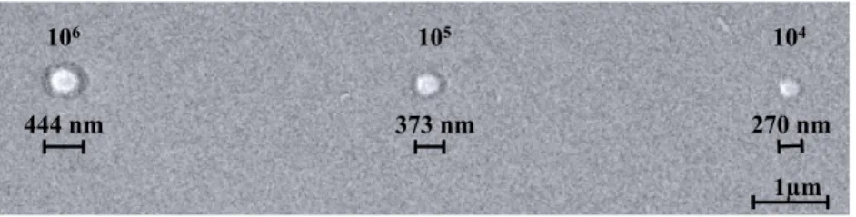
The subsequent decrease of energy per pulse and/or number of pulses gives rise to nano-hills formation. The tiny nano-hills (see Fig. 4) can be attributed to laser damaged zone. The similar
effect was observed in fused silica in a single-shot regime [42]. The size of the damaged zone is 10 times smaller than the beam size.
106 105 104
1µm
444 nm 373 nm 270 nm
Fig. 4. Increase of the diameter with number of pulses due to defects accumulation (Epulse=
21.7 nJ). Zone C in Fig. 2.
The increasing diameter of nano-hills with number of pulses puts in evidence the effect of threshold to induce chemical modifications of the material. Defects are accumulated while acquiring an increasing number of pulses from 270 nm to 444 nm in diameter for 104to 106 pulses with pulse energy of 21.7 nJ. In this case we speak of the absorbed dose (D) putting in evidence defect accumulation D = EN, where E - incident energy and N - number of incident pulses. Laser absorption increases with the laser induced defects amount in fused silica [19, 20, 43] and soda lime glass [32, 34]. It is widely discussed that the local temperature increase can be around glass transition temperature Tgin sodium aluminosilicate glass in the laser irradiated zone of high repetition rate lasers. We estimate that the temperature increase in the interaction volume is lower then Tg, thus making the interaction process athermal in this particular case.
The origin of those nano-hills is unclear. The surface nano-hills formation is a signature on the increase of volume. The description of the defect formation and relaxation in a multicompo-nent silicate glass is not an easy task. Trukhin et al. [45] in a systematic study on the presence of sodium or aluminium in silica under UV exposure have shown that the defect formations are different as compared to pure silica. In the case of sodium containing glass, the defects are mainly driven by the presence of Si–O–Na+groups called L groups. Lonzaga et al. have also discussed that in soda lime glass color centers produced under femtosecond laser irradiation are mainly trapped hole centers resulting from the existence of nonbonding (NBO) oxygen involve in Si–O–Na+groups [34]. They have identified two centers H+2 and H+3 with absorption at 460 nm and 620 nm respectively. The identification of the electron centers remains difficult. Never-theless, the stability of the defect relies on the maintening of the charge separation. Transition ions such as iron, in our case in low level, are well known also for participating to the defect stabilization due to their two degree of oxydation in glass Fe2+ and Fe3+. Fe3+have been re-ported, for instance to act as an efficient electron trap [46]. As a conclusion, it appears that the type and the photoinduced defect concentration in glass is function on alkali and alkaline earth ions [45] and their stabilization could be function on other ions such as transition ions which offer different degree of oxidation [47].
3.2. Direct laser writing and the KOH etching
For low deposited energy value, the dielectric function of the material is slightly modified that could cause some transient or permanent modifications (phase change, local refractive index change, chemical reorganization), but without any visible topography change. In our case these structural modifications are revealed using KOH wet etching. The effect of KOH on laser modified region for 1 or 2 minutes is negligible and can be compared with surface cleaning. But starting from 5 minutes of etching in potassium hydroxide the laser structured zone undergoes modifications especially in the direction perpendicular to polarization state [39]. In the case of
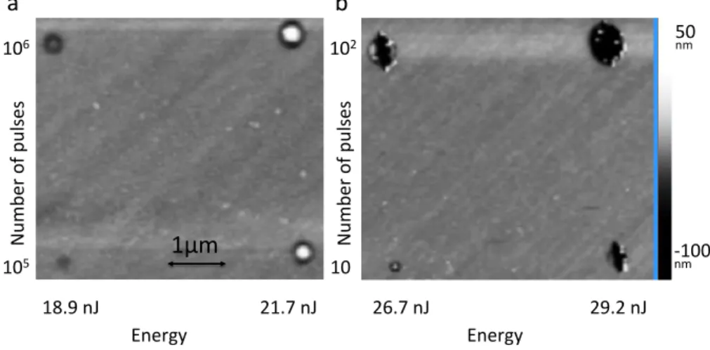
strong ablation crater diameter and depth becomes larger. In Fig. 5 are presented AFM images of the surface topography after 10 min in KOH.
a
b
1µm
105 106 10 50 nm 18.9 nJ 21.7 nJ 26.7 nJ 29.2 nJ 102 -‐100 nm Energy Energy Nu mb er of pulse s Nu mb er of pulse sFig. 5. (a) - (b) AFM images after 10 min in KOH respectively of nano-craters revealed
after wet surface etching(105and 106pulses@18.9 nJ) and nano-hills for 105and 106pulses
with energies 21.7 nJ per pulse; nano-hill (10 pulses, 26.7 nJ per pulse) and polarisation
dependent ablation at energies of 26.7 and 29.2 nJ with 10 and 102pulses.
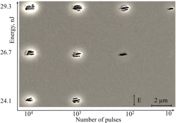
The nano-craters independent on polarization, which are revealed after wet surface etching for high number of pulses (105and 106) with energies 16.5 (not shown here) and 18.9 nJ per pulse have the diameter of ∼ 250-300 nm and the depth of 5-10 nm (see Fig. 5(a)). The nano-hills also independent on incident state of polarization have the diameter of 350-400 nm and the height of 45 nm (energy 21.7 and 105and 106pulses). They are affected by etching revealing the etched rim surrounding the hill (see Fig. 5 bottom image). The nano-hill is produced by low number of pulses (10) and low energy 26.7 nJ per pulse (diameter 200 nm, height 35 nm) in Fig. 5(b). The KOH etching decreases the height of the structure: 35 nm after etching compared to 45 nm before. The etching effect is more pronounced for nano-gratings where the contrast between the aspect in length 1 to 6 (parallel to perpendicular to incident polarization direction) becomes 2 to 6 after 10 min in KOH for low number of pulses. Figure 5(b) shows the modifications for energies of 26.7 and 29.2 nJ per pulse and 10 and 102pulses. The structure width along the polarization direction is 200 nm, the length, perpendicular to the polarization direction is 600 nm with a depth of 55 nm. In addition, the linear shape of a nano-grating turns into the one affected by etching with irregular border (see Fig. 6 for 102pulses).
To conclude, the incubation and positive-feedback proposed by F. Liang, R. Vall´ee et al. allows to explain the creation of circular nano-hills and etched craters of a tiny size which are not sensitive to the laser polarization state in the zones B and C in Fig. 2. The threshold of material modification for nano-hill and nano-crater production is governed mostly by the absorbed energy dose. The size of the final structure is mostly defined by the number of incident pulses. Further increase of the incident energy and/or number of pulses drives to the significant increase of laser-induced defects induced by laser thus to the exaltation of photonic effects. Spatio-temporal intensity distribution becomes crucial. Nano-gratings starting from one central line oriented in accordance with optical field direction are produced in this conditions (zone D in Fig. 2). If the energy is increased once more, the circular craters non-sensitive to polarization state are obtained followed by the strong ablation with a rim surrounding the crater (zone E in Fig. 2).
#193141 - $15.00 USD Received 4 Jul 2013; revised 23 Oct 2013; accepted 26 Oct 2013; published 18 Nov 2013
2 µm E Ener gy , nJ Number of pulses 10 10 2 103 104 24.1 26.7 29.3
Fig. 6. Nano-gratings after 10 min of KOH etching (10 to 104pulses from right to left).
The direction of the electric filed is shown by an arrow. Zone A, B, C, D in Fig. 2.
From the applied point of view the structures (gratings, hills and nano-craters) produced with low and/or high number of pulses can be used for photonics purposes. Data storage with a standard DVD recorder demands the speed (34.9 m/s for reading and up to 16x for writing) and the tight specification for compatibility of the formate sizes. The informa-tion coding is performed by the inscripinforma-tion of sequences with different lengths. The size of the smallest DVD sequence called pit T3means 3 dots of T1size (133 nm). T1size is multiplied by an integer number (from 3 to 11 for DVD) to define the total length of the pit. Thus the smallest DVD pit is 350 nm wide and 400 nm long. The controlled inscription of seed nanometric mod-ification is suitable for DVD, Blue-Ray and future formats. For data storage compatible DVD formate the nano-hills and nano-craters are suitable as they are easily produced with low (10) number of pulses corresponding to DVD writing with 1 GHz repetition rate laser. The surface patterning and chemical passive etching suit for the production of the GlassMaster disc, which allows to produce its replicas called Nickel Stamper that are then used for pressing a DVD from heated polycarbonate in classical production line.
4. Conclusion
We have demonstrated different zones of interaction according to incident laser parameters for high repetition rate femtosecond lasers in sodium aluminosilcate glass. Surface modifica-tions vary from the photochemical material modification to strong ablation with a surface rim formation induced by shock waves. Post-direct laser writing chemical treatment for further development of laser modified region assures the inscription of nano-patterns independent on polarization. The material photochemical reorganization allows achieving 200 nm sized craters (femtosecond laser @ 1030 nm and NA=0.7), which can be used for photonics or long-term data storage. In the intermediate zone, the damaged zone with the local density alteration pro-duces nano-hills with the height of several tens of nm. The nano-gratings are formed by in-cubation effect creating defects and plasmonic effect, which affects the dielectric function and thus alters locally laser intensity distribution creating minima et maxima of the intensity thus producing nano-grooves. One can directly write a single nano-groove with the aspect 6 to 1 in length (perpendicular to parallel direction to incident polarization one). Thus we reveal the controlled inscription of nanometric modification compatible with DVD, Blue-Ray writing and future formats.
Acknowledgments
Financial support of the Projects ”FELINS” and ”ARCHIVE & FORGET”, the Region Aquitaine and Department of Gironde is gratefully acknowledged. The authors thank C. Boy-aval for the aquisition of SEM image and M. Lahaye for the measurement of the glass compo-sition.
#193141 - $15.00 USD Received 4 Jul 2013; revised 23 Oct 2013; accepted 26 Oct 2013; published 18 Nov 2013