HAL Id: hal-02523157
https://hal.archives-ouvertes.fr/hal-02523157
Submitted on 28 Mar 2020
HAL is a multi-disciplinary open access
archive for the deposit and dissemination of
sci-entific research documents, whether they are
pub-lished or not. The documents may come from
teaching and research institutions in France or
abroad, or from public or private research centers.
L’archive ouverte pluridisciplinaire HAL, est
destinée au dépôt et à la diffusion de documents
scientifiques de niveau recherche, publiés ou non,
émanant des établissements d’enseignement et de
recherche français ou étrangers, des laboratoires
publics ou privés.
A model of GTO compatible with power circuit
simulation
Corinne Alonso, Thierry Meynard, Henri Foch, Christophe Batard, Hubert
Piquet
To cite this version:
Corinne Alonso, Thierry Meynard, Henri Foch, Christophe Batard, Hubert Piquet. A model of GTO
compatible with power circuit simulation. 5th European Conference on Power Electronics and
Appli-cations, EPE’93, Sep 1993, Brighton, United Kingdom. �hal-02523157�
1
About 6ftea1 y u n ago. the chakngc of s~ulaSion in beh.viour of vpions topologies of converters. A ruaple
b i i resistor
M m )
was enough to y t the c b n c t c n d c s of s given converter with s VQY goodr c ~ a c y (peak md R M S currents. outpot power. output Nowadays, the ever increasing calculation power of computers allows representing the switches more accurately to aid the design of the switching section (design of the s n u b . pndiction of the current and
voltage overshoots. study and optimiiution of the losses in the switches 7.
...).
However. the modelling techniqucr u e cat.inly not that advanced ; on the one hand. some physics-rooted models allow predicting the device behaviour but the simulated circuit must be very simple ( k a q (I)), and on the otha
hand
c o n p " ~ t a l models um be used inmonrealistic circuits but they might be wrong in spacial operating modes.Our tpproach is an attempt to put basic physics in a circuit-
type model that could be used in a static converter
simulation software.
p o w a d ~ w u to pedictmdlmdcrrtmdthc
e
0pCmion.of my switching device md dcrrrmme the
nuia
ChUWCliStiCS. ...).
workshave already bacn
caniad
out in ow team on mis subject and a model has bwn proposed for the PN junction and applied for the bipolar tramistor (Batpd (2) a d Batard (3)).As
a first step, we will describe brienythis
model of a PN junction. Then, we will show how this modcl can help modelling a multi-junction component like theGTO
thyristor.
PN JUNCTION
MODELLINGIn power electronics applications the important characteristics of a diode me :
-
the low on-state voltage as a function of the forward - a tIf,
-
the low reverse current in off-state as II function of thereverse bias.
V
- l l l c c " n masc ~ a y c l p r r a t b , a t a r m o & .
-
the ranaling of the curralt .pia L ( s o f t or mapoff~ v i o u r ~
-
the lq$lIid voltrge (dv/dt) at tpmoftEach of tbeM chuactc&tica U modelled U r'rmply as posnic. For exampk, though it
is
possible to model the V(l) static chsracteristicswith
one or s e v d threshold voltagc(s) and s variable series resistor, we wiU keep theusual R,JRarcpr~ta!im which is icaptabk in most of our applications.
What we will try to i m p v e is thc r e m o f o f t h e chalges which m of high interest in power a p p a
lhese
charges are reprrsented by a parallel rrp.cim ; it is well known that the charges arc not a linear M o n of thc voltage, which can be intupreted as a variable capacitor. Fonnu studies rhowed tlut a two-state capacitor (C,/C,)charges versus voltage. To avoid a u r g y dkwnrinuity the
wmmutation between the two capacitors must be done a$ thc very
moment
when the junction commu- from the On-statc to the off-state md vice-vuxr For thisreason. the
modcloffigurrlwasinfroducad
gives a fairly good nprrrmtul 'on of the vnipion of the
,
Cr
I
I
K4
Figure 1 : Model of a
PN
junctlonA v a y smaU inductor is amnected
in
saies with the binary resistor to create a voltage dmp proportional with the Q 1993 The European Power Electronics Association233
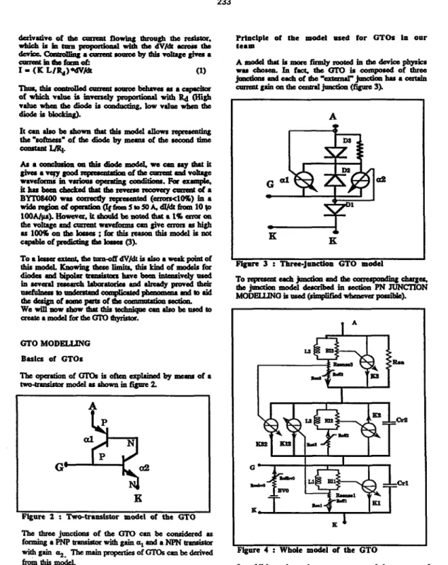
GTO MODELUNG B a l e s of GTOs
The opcntionof GKk is
oftea
cxphilledby" of at w o ~ d U r b o w n i n ~ 2
K
Flgurc 2 : Two-tr;mnslstor model of the GTO
G
c
A
I
Figure 3 : Three-~unctlm GTO
model
L.b.0
BrP.1
Gm
KThis piecewise linur model fm be owridered as m poor
representation of the strong non-lincaritics of red GTor
(3). Howeva, it lus the advantage of being dhadly usable in simulators involving otha caqn" madcucd with
the ume precision. I t is upable of rhoviry the main phalolll-nktcd to mco"ut8ti~nrchrr currmt
tail
Ipa
and spike voltagev,
Thir
model (figurc 4)is
only qualitative. In order tobcen developed. It will be cxpl8ined in the next reaiolt d e t e r " dl of its pmmetcrr. a rystanatic muhod has
PARAMETERS
IDENTIFICATIONGivm themrmbaof p.r9ncw m the model, a systematic
O M .
An objaCtive m QUI mcthod is to ibtify eachmethodisnasdbdtodctcnninememodelpPrmdcrrofthe
paranetcr,repaucly 6rom
mc
OthCzE. so. rpecirl tests toevaluate jimction by jmlaim the vducs of the diffffcnt
p m - have been developed
In
this section, these tests and the corresponding parameters iddicatim are detailed. Some of theroughly the same value for a given punetcr. the confidence m the
pp.mercn
model is incruced But they will M t be dctribdhac
~xpatnmtrl muhod Carmot be M yextended to gold-
parameters um be dctamind by otkrr teste.
If
urey
give ~ h c mowing method duls with mod-mos.
T ~ L
dopcd GTOs beuose come parameters m the central
junc&mof gold doped
mos
C " t be munrred from the tenniuab.T h e GTO
uuda test is ratedbag,,
= 6 0 0 A.V,,=1600V. I t s v e d e t a r m n e d for a given
tunperaanr. Wndy 25T.
Identlflcatlon of the parameters In the anode J u n c t i o n
In a
GTO.
the measurable qumtities arc the mode c ~ c n f 1..the gate CMaIt I'. the
-
voltagev,
and the gateuthode VOlUge VgkThe
fm
test ic b w d on these four values.I-
I
&:
-
'Igure 5 : chopper circuit used for tests The simplest circuit including switching of a G M is
s h ~ d i c d : a chopper (figure 5). The
GTO
is ptcctad by a 1pP snubber at turn-off. In order to reveal the trtrinSicbehaviour of the
GTO.
mubberless opaation will also bestudidinthcfollowiug. For this reason, this choppa has
to be a high m o wvoltage design Thc frae-whccling diode used in the chopper is rated
b(AV,
= 300 A, V,=400Vand its Q= irvcry low (Q,-4pC).Thii
design makes the choppcr the w m t component of this
chopper which is the best way to test the
GTO:
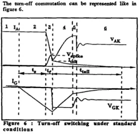
dl theothexcompo~1tscu1becc4nidawj II idulannpomata The mm-off commutation CUI be represented like
in
figure 6.I
Figure 6 : Turnoff swltchlng under rtandarc c o n d l t l o n s
Determining
K3,
L3,
Q.
At the beginning ofmode
3.
V
,
,
.ppurr as the central junction t u n c off. The begiuningof mode 4 is dc6ned .s rhe timc whm the gate cubodejlmdion " S O &so.
duringbody
memodcjunction
isconducting
md at th.ttime. the clurges storedinthisjunctioncallbededuced
With this ch0pp.S. s e v a a l points of operation w1 be
chosm. In this d o n , the more important is to have the same pint for all the tests. We ChmKe
IM=
180 AwithEh-
= 125V.
At this point. = 7p.It
canbe YQLin
the model that :t
= 3 @.no + RrenrJ)c,
with C,. the forwud capacitance representing charges
Srored in the .nodejlmction Its vduc can be d a i v d from relation :
c,
= K3*% (3)Substimting for C, from cqusrion (3)
in
equation (1). weCM determine K3*L-,. I,#$, must be a v a y low time c(NtanL If
r,
= 1nH.
we getK3 = 2333.Determining K32. Physically. unong the carriers
injected through the anode junction, those which do not
r-bm cxeate a reverse current through the central
junction This c-t gain is represented by a, in the
model of figure 3 and by a ammlled current source I
,
,
with its gainK32
in the modcl of figure 4. The relation betwemthanis:( 4 )
To
establish this rclarion. we suppose that the short-circuitist tor
R,,
ud the anode j u u c t i o n R d + b arcequal. In order to determine a,. the same test than bcfore was used.In
fact,a,
C I L ~ be roughly deducedf"
figure 6.I)laing
the conduaion. the current I, creates through thecentral junction a reverse cunmt
(J32).
its value is a1*
I,. K32 = 2 a,/Rd
235
The value of I , at thc beginning of modc 3 will be nolad
I,,yI, at the b e eof mode 4 will be ~ t s d
b.
AtthismnneaSd~themodcjunction~fonducMg . A s t f
(fall timeof
y
is vcry d compced to r&l. theamattc o n s i d c r e d ~ to I32 xfwcmeasrne&) m d h . we can
r,
a1*% ( 5 )R2 is roughly mnrtmt during modc 3. So.
&tamhe a1 with &dation (5).
can be
Then.
at the & S e n point,b =
14.5 A.I,
= 180 A. So.al = 0.08.
Thc values of the modcparmctQv uelistalklow : L3=lnH
&=loo
a
&=0.5d
P , , = 0 , 5 & L=lmaK3=2330
K32
=
322In
addition to the puunetar of the mode junctio~ thisrcstbclpr deriving (bepmsitic indunaof the mnbba (YJ &om therpJrevolrycv.pJso’
With dI,/dt=533 Alps ~ I K I V ~ E : 63
V.
I, = 0.12 pH.For
the p a r m a a sin the otha junctions.
more specifictcsts must be carried out
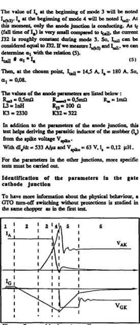
Identlflcatlon of the parameters In the gate cathode Jonctlon
To have marc infomation about the physical bch.viour, a
GTO
hun-off switching without potcctions is rmdicd m thesamechoppa r s m t h c f i n t t c a I I I I.
* .I
rigure 7 : snubberless turn-off
The ovavoltage is now proportional to the load cwcnt. The l i t a t i o n of the overvoltage at turn off without
protections for our application is Vwe (for this GTO. V = 400 V). So. a low input voltage l i e
Eh,,,,,
= 125 V allows snubberless operation of theGTO
which is the k t way to char- the
GTO
itself. The snubberless aml-off is rqxcrcnted in figure 7.Determlnlng
K1,
L,, R,,.The determination of the gate cathode parameters can be made if the voltage md the current through the junction are known. The voltage is m ddirectly L( theG
and K taminals. But themust be determined indirectly. From figure 3. we have :
4
=5
+b1=
4
1 1 1
I 1 1
. .
VGKFigure 8 : current and voltage of the gate cathode Juactlou
The waveforms in figure 8 allow the d e t a m i o n of the
charges rtoredm the g.tMthodcjunCtioh
4,
= 180 A, dl&t = 711 A&,I,,,,,
= -75 A.We fix&
= 1 nH m d h = 100a, Then K1= 110. Determlnlog C,, and Ctz.With
this typc ofjlmaioa
In mode
5 of the snubbaless ammutath.V,,
(figure 5 ) is determined in othm tests. Musuriag the puiod
T,
of theV
,
osciUation. the revase capacitance ofQrmmUtatian (figure
71
we cm Jsodetcrmine
tbe mQEccq”as
of mccmetljrmction d o t the gucuaodc
aKillatcs. The paTasit inductma of the power cirmit
4
dre CcnmljMCtion C, can be detamined
4
= 0.35 p 9T,
= 2185 N. then C, = 3.5 nF.A similar process gives the revaxe capacitmcc ofthe gate
uthodc junction Crl. Thc paiod
TI
of the Vlt oscillation is “ r e d in mode 6 md with~detmnincdbeforq the value ofc,
is dctamincdlo
= 0.25 pH.T,
= 515nr.
then C, = 27 nF. Determlnlng BVO for the gate cathode Junction. The value of this Lwskdawn voltage is k t l ysimulated by a voltage source d m ideal diode. BVO=-18V. L a = 0 . 5 ~ . Rotfbro=10l(Q
The
parametas of the gate cathode junctions are :& w = O . s m Q ,
&=lo4a
L,=O.SIILQ L ~ = O . ~ I I L Q ,
Bv,=
- 1 8 Vr,
= I d . Rll = 100n,
K1 = 110With these parameters. we have all of the gate cathode
paramaas except the forward gain K12 of the current
source J 1 2 K12 reprMlts directly %.
Identlflcatlon of tbe parameters In the central Junction
For
the central junction, one solution involves forcing thir junction to work in the forwd mode.m
r
T
E4Ip.t-Id-
G M teatedI
I I F l e n r e 9 : ChoDpcr c i r c u i t modified f o r d e ~ e r m l n i n g ccntrai -parametersIn faq it is 0pcr.tCd as a " b w k e l i n g diode". Then, the
GTO ccntnl junction conducts in forward mode while the
two other jrmctions are inhibited
The urpaimentll ret-up is the same choppa in which the freewheeling diodc is replaced with the GTQ thyristor. The gatc cathode jlmction. it is rhort-circuited as close to the CIJt as pwribl&,nKqthecmrenr ins& them0 is forced
are not oonduaing 10 that the gains are not activated. n e global Circuit is rrprarented in figure 9.
To
neutralim theso thu it flows thmugh the antral junction ud the mode
short It should be noted that the mode md gate junctions dI/dt is limitsdby a& inductor and load cllncnt is 10 A (a rough estimation of the current flowing through the
central diodc of the model in n doperation).
I
I
I
as
p s l d i rI
Figure 10 : Current and voltage through the
central junction
The experimatal current and voltage are shown in figure 10. The maximum reverse rccovery current
I,,,,,
= -20 A andthe "softness" time 4 = 425 ps corresponding to the
initial current &o= 10 A and a dUdt of 13.3 A/ps allow
determining
b,
RE
and IC2 of the central junctionD
,
.
We obtain:
L2=lnH
R
,
= 4mfl K2 = 2900Roc,z = 0 . 5 d
&
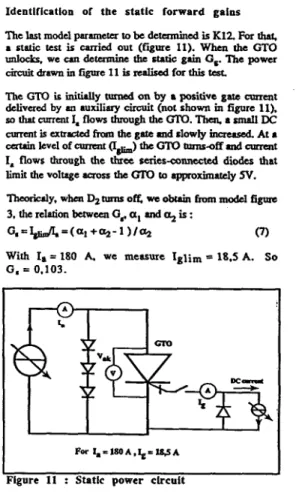
= 10% tf= 0.ZpIdentlflcatlon of the static forward galas The last model parameter to be detamined is
K1Z For
that, a static test is carried out (fGure 11). When theGTO
unlocks. we can detamine the static gain 0, The power circuit drawnin fgure 11 is realised forthis testThe GTO is initially
trmMd
on by a positive gate current delivered by an auxiliary circuit (not shown in figure 11).bo thatcurrentl, flows thmugh the
OM.
Then. a smallDC
cllrrult is a t r d from the gate and slowly incrrrsad At a I, flows through the three s~esoonnected diodes that 0at.in kvelofalrmu (I*) thecm tmns-off mdanrent limit the voltage across the OM ta approximately N.
?heoriuy, when D z m o & w c o b t h
fro"&
figure 3. the relation between 0,al
andg,
is :G , = b , , J I . = ( a l + a z - l ) l a , (7)
With 1. = 180 k wc measure I g l i m = 18.5 A.
G. = 0,103.
SO
For b = 1 8 0 A , $ = W , 5 A Figure 11 : StatIc power clrcuit
To reduce the on-voltage drop of the
GTO.
the NIU al+
%must be maximized. However. a y must be as low (IS
possible to limit the current tail. (see section Basics of
C r o s ) . So, az must be close to 1. Assuming az = 1. gives
G, = al = 0.10. This value is to be compared to that derived
from the c w e n t tail measurement (a, = 0.08). The dif€crcncc between
these
two vducs (roughly 20%) can beeasily explained by the measurement of which is very dimcult to achieve (offset, ringings. ...).
The values used in the simulation presented in the
following section are :
%'1. a1 = 0.08,
K12 = 2000. K32 = 322. Identlflcation conclusion.
We have determined all of the GTO model parameters in this pah The sccond point of the study is the global validation of the model. So we fur the model with its parameters and we place this model in its simulation environment.
In the next rection we describe how we validate the model and its Iits. It should be noted that the parameters of the model used are those given by the method described above
and they are never modified to achieve some sort of "curve- fitting".
237
E X P E R I M E N T A L AND S I M U L A T E D WAVEFORMS COMPARED.
Fmt. we validate the model at the same point &Osm for the
p
a
"
-on. Then with fued parametar.c e v d sunulat~onr are made at different voltage and
current
levclr. F i i y . we
compare the experimental andS hred&. ~
For example. a turn-off of the real GTO and its
a m x p o d q simulation are represented in figurer 12 and
13. Figure 12 displays the upcrimentll results obtained
attrrmoff wimamnbba.Thicis .chievedat 125 vinplt v01t.g~ md 180
A bad
current. The initial dfg/dt is4ONw. m d h is equal to 7% This can be considaed
as a fast turn-off with a aun-off gain of only 2. The snubba is composed of a 1pF capacitor md a 1SR resistor.
'lgnrc 12 : Experlmental turn-off of a GTO
xia4 t w1.1
r'igure U : Slmuhtlon turn-off of a GTO
Figure 13 shows the turn-off simulation results obtained with a 1pF snubber,
h =
180 A. &= 125 V. As can be seenf
"
these
waveforms. the main phmomma are r e p r d and have a reasunable amplitude.Wi
the different simulations made, we can directly compare simulated current and voltage values with experimmtal results.For
example, M have :dlJd& = 560 Alps.
&=75 A. =70 A.
The figures 14 and 15 s u m up the behaviour of several variables ovff a wide region of 0Per;ltion.
For the snubbcrlle~ opaation a similar study is made with
experimental and simulated d t scompared. W d b , = 525 Alp ;
a o zo 40 60 m am tm I ~ O 16a
rIgure
Is
: Experlmental and simulatedIgm
compand (Irrm)CONCLUSION
We can say that most quantities are in agreemeat with
cxpuimental d t sbut there remains certain difficulties Concaning dV/dts
in
snubbaless 0per.tiOns.This particular operation is not used in conventional
opention. in p d c u l a r when it is necessary to optimisc
the power ckuit, Presently. we -I have a good idea of brsa but M predict the global behaviour.
REFERENCES
1. Leturq.
Ph.
Khati~.2,
Gaubea. I.. 1989. Rechachc Transport SecuritC. juin 89."Simulation des thyistors Gate-Turn-OK "
2. Batard, C.. Meynard, T.A.. Foch
H..
Massol. J.L., 1991. Con& EPE 91 Florence-.SUCCESS. Application to diodes and bipolar transiston." 3. Baud, C.. 1992,.Th& de doaeur de I T " Toulouse. " Interactions composants-circuits dans les onduleurs de
rension.Carscterisarion-ModelisationSimun. *
4. P.scal.J.P,.1986. Th&sc de doctorat &&at es Sciences Physiques prhnb5e i I'universib5 Pierre et Marie CURIE.
Paris
VI." Etude des circuits &aide
i
la commutation de thyristors GTO mont.5 en d i e pour des applicationsferrOViaic. "
'ciicuit-oxialtcd Simulation of power saniconductor using