Development of ultracompact, high-sensitivity, space-based instrumentation
for far-infrared and submillimeter astronomy
ARCHIME
byMASSACHUSETTS INSTITUTE
Giuseppe Cataldo OF TECHNOLOLGY
B.S., Politecnico di Milano (2007)
M.S., Politecnico di Milano (2010)
JUN
232015
M.S., Politecnico di Torino (2010)M.S., ISAE-SUPAERO (2010)
LIBRARIES
Submitted to the Department of Aeronautics and Astronautics in Partial Fulfillment of the Requirements for the Degree of
Doctor of Philosophy at the
Massachusetts Institute of Technology
June 2015
2015 Giuseppe Cataldo. All rights reserved.
The author hereby grants to MIT permission to reproduce and to distribute publicly paper and electronic copies of this thesis document in whole or in part in any medium now known or
hereafter created. Signature of Author Certified by... Certified b iy Certified by Certified by Accepted by
Signature redacted
Department of Aeronautics and Astronautics
S a
redacted%#-k
March 5, 2015S ig a
tu e r d
a c e d
...
\% Jeffrey A. Hoffman
es r of the Practice of Aeronautics and Astronautics
Sig nature redacted
Thesis Supervisor... ...
Kerri L. Cahoy
Agistjift IVrpfyssor of,4ronautics and Astronautics
...
S i
a u r
Seidaattud
...
. ) I Samuel H. Moseley
Signature redacted
/Aenior
Astrophysicist, NASA . . . .. . . ... . . . . ... . . . ...Edward J. Wollack
S
gResearch
Astrophysicist, NASA.... ,S g a u e r d c e
...
Paulo C. Lozano
Asso iate Professor of Aeronautics and Astronuatics Chair, Graduate Program Committee
Development of ultracompact, high-sensitivity, space-based instrumentation for far-infrared and submillimeter astronomy
by
Giuseppe Cataldo
Submitted to the Department of Aeronautics and Astronautics on March 30, 2015 in Partial Fulfillment of the
Requirements for the Degree of Doctor of Philosophy in Aeronautics and Astronautics
ABSTRACT
Far-infrared (IR) and submillimeter (15 pm-1 mm) spectroscopy provides a powerful tool to probe a wide range of environments in the universe. In the past thirty years, many space-based observatories have opened the far-IR window to the universe, providing unique insights into several astrophysical processes related to the evolution of the early universe. Nonetheless, the size and cost of the cryogenic spectrometers required to carry out such measurements have been a limiting factor in our ability to fully explore this rich spectral region and answer questions regarding the very first moments of the universe. Among the key technologies required to enable this science are ultra-low-noise, far-IR, direct-detection spectrometers.
In this thesis, Micro-Spec (p-Spec) is proposed as a novel technology concept to enable a large range of flight missions that would otherwise be challenging due to the large size of current instruments and the required spectral resolution and sensitivity. p-Spec is a direct-detection spectrometer operating in the 450-1000-yim regime, which employs superconduct-ing microstrip transmission lines to achieve a resolution (1Z > 1200) and be integrated on a
S10-cm2 silicon chip.
The objective of this thesis is to explore the feasibility of the P-Spec technology. First, analytical models are developed for the dielectric function of silicon compounds to be used as substrates in the transmission lines. These materials represent the ultimate source of loss in the system. The models are used to analyze laboratory spectral data of silicon nitride and oxide films and provide information on the loss within a 4% accuracy. A design method-ology is then developed for the spectrometer diffractive region given specific requirements on size and spectral range. This methodology is used to explore the design space and find the optimal solutions that maximize the instrument efficiency and minimize the phase error on the focal plane. Five designs are described with different requirements and performance. Finally, analysis and calibration techniques are developed to study the properties of the su-perconducting materials employed in the transmission lines and detectors. These techniques are applied to laboratory data of molybdenum nitride and niobium to extract their quality factors and kinetic inductance fraction within a 1% accuracy.
Thesis Supervisor and Committee Chair: Jeffrey A. Hoffman, Ph.D.
Professor of the Practice of Aeronautics and Astronautics MIT Department of Aeronautics and Astronautics
Thesis Committee Member: Kerri L. Cahoy, Ph.D.
Assistant Professor of Aeronautics and Astronautics MIT Department of Aeronautics and Astronautics Thesis Committee Member:
Samuel H. Moseley, Ph.D. Senior Astrophysicist
NASA Goddard Space Flight Center
Thesis Committee Member: Edward J. Wollack, Ph.D. Research Astrophysicist
NASA Goddard Space Flight Center
Thesis Reader:
Robert Simcoe, Ph.D.
Associate Professor of Physics MIT Astrophysics Division Thesis Reader:
Omid Noroozian, Ph.D.
NASA Postdoctoral Program Fellow NASA Goddard Space Flight Center
Acknowledgments
This thesis is dedicated to my parents, whose unconditional love and sacrifices have ultimately allowed me to achieve this and other important milestones throughout my life. Infinite thanks go to my wife-to-be, Maria, for taking on all the challenges of a long-distance relationship during my two years in Cambridge and supporting my endeavors through the end.
I enjoyed being part of the Man Vehicle Lab and Space Systems Lab, many of whose
members shared with me overnight or weekend efforts always with a smile on their face.
My involvement with the MIT community was also a unique way to develop new friendships,
from being resident and secretary in The Warehouse and a member of the MIT Tech Catholic Community to sailing, skiing and scuba-diving.
Special thanks to my advisor, Prof. Jeff Hoffman, for his guidance, kindliness and constant support and to my co-advisors at NASA, Dr. Harvey Moseley and Dr. Ed Wollack, for all the helpful advice provided along these years and for pushing me to always learn more and think out of the box.
This work was supported and funded by the Massachusetts Institute of Technology's Arthur Gelb fellowship and the National Aeronautics and Space Administration's Research Opportunities in Space and Earth Sciences (ROSES) and Astronomy and Physics Research and Analysis (APRA) programs.
Table of contents
1 Introduction
1.1 The importance of infrared astronomy and the need for space telescopes . . .
2 Problem statement and objectives
2.1 Existing gaps and future needs . . . . 2.2 Filling the gaps with Micro-Spec . . . .
2.3 T hesis objectives . . . . 2.4 T hesis outline . . . .
3 p-Spec transmission lines: materials characterization
3.1 The complex dielectric function . . . .
3.2 Analysis of the dielectric properties of silicon nitride thin films . . . .
3.3 Analysis of the dielectric properties of silicon oxide membranes . . . . 3.4 Sum m ary of findings . . . .
4 p-Spec multimode region: design and analysis
4.1 Literature review of spectrography . . . .
4.2 Design methodology . . . .
4.3 Low-resolution 3-stigmatic-point solution . . . .
4.3.1 Antenna feed response . . . . 4.3.2 Antenna array response . . . .
4.3.3 The R65 built hardware . . . . 4.4 Higher-resolution 3-stigmatic-point solutions . .
13 15 21 21 26 30 32 33 34 35 41 48 49 . . . . 5 0 . . . . 5 3 . . . . 5 4 . . . . 6 1 . . . . 6 2 . . . . 6 6 . . . . 6 7
4.4.1 Problem formulation . . . . 4.4.2 Optimization results . . . .
4.4.3 Power coupling efficiency . . . . 4.4.4 Summary of findings . . . . 4.5 Higher-resolution 4-stigmatic-point solution . . .
4.5.1 Problem formulation . . . . 4.5.2 Optimization results . . . . 4.5.3 Power coupling efficiency . . . . 4.5.4 Summary of findings . . . . 4.5.5 Revised higher-resolution 4-stigmatic-point
. . . . 6 7 . . . . 7 1 . . . . 74 . . . . 74 . . . . 76 . . . . 76 . . . . 79 . . . . 8 1 . . . . 8 1 solution . . . . 81
5 p-Spec detectors: modeling of superconductors' response 5.1 Microwave kinetic inductance detectors . . . . 5.2 Literature review of resonator response modeling techniques 5.3 Analysis and calibration of superconducting resonators . . . 5.3.1 VNA transmission data calibration . . . . 5.3.2 Phenomenological resonator model . . . . 5.3.3 ABCD-matrix model . . . . 5.4 Summary of findings . . . . 6 Conclusions 6.1 Thesis summary. . . . . 6.2 Contributions . . . . 6.3 Future work . . . . Bibliography . . . . 83 . . . . 83 . . . . 87 . . . . 88 . . . . 88 . . . . 91 . . . . 95 . . . . 100 105 105 107 109 111
List of Figures
1.1 The electromagnetic spectrum . . . . 14
1.2 The energy distribution in the universe . . . . 16
1.3 Interstellar dust processes . . . . 17
1.4 The Carina nebula . . . . 18
2.1 Layout of the p-Spec module . . . . 26
2.2 Sensitivities of state-of-the-art ground and space telescopes . . . . 27
2.3 Geometry of a microstrip transmission line . . . . 28
2.4 Block diagram of the p-Spec module . . . . 30
3.1 Room-temperature transmission of a silicon nitride sample 0.5 pm thick . . . 37
3.2 Measured and modeled transmission for a 3-layer stack of silicon nitride sam-ples 2.3 pm thick . . . . 38
3.3 Real and imaginary parts of the dielectric function of a silicon nitride sample 0.5 pm thick . . . . 40
3.4 Room-temperature transmission of a silicon oxide sample 1.0 pm thick . . . 41
3.5 Real and imaginary parts of simulated dielectric functions for the three models discussed . . . . . 44
3.6 Simulated transmission functions for the three models discussed. . . . . 45
3.7 Real and imaginary parts of the dielectric function of a silicon oxide sample 1.0 pm thick . . . . 46
3.8 Real and imaginary parts of the complex refractive index of a silicon oxide sam ple 1.0 pm thick . . . . 47
4.1 Geometry of the Rowland grating . . . . 50
4.2 Review of the main literature in spectrography . . . . 51
4.3 The Z-Spec hardware . . . . 52
4.4 Simplified representation of the Micro-Spec grating geometry . . . . 56
4.5 RMS phase error for the R65A design . . . . 60
4.6 Feed horn angular response at 430 GHz (left) and cross section of the parallel-plate waveguide and microstrip transmission line geometries (right) . . . . . 62
4.7 Power distribution in the multimode region at 450 GHz . . . . 64
4.8 Design R65B angular response . . . . 66
4.9 The Micro-Spec R65 hardware . . . . 67
4.10 Objective spaces for Design R260 . . . . 70
4.11 Objective spaces for Design R520 . . . . 70
4.12 Multimode region design for Designs R260 and R520 . . . . 72
4.13 RMS phase error for Designs R260 and R520 . . . . 73
4.14 Coupling efficiency of the R260 and R520 designs . . . . 75
4.15 Objective spaces for Design R257 in first order . . . . 78
4.16 Optimized multimode region for Design R257 in first order . . . . 79
4.17 RMS phase error for Design R257 in first order . . . . 80
4.18 RMS phase error for Design R257 in first order . . . . 82
5.1 A lumped-element circuit representation of a MKID and its detection principle 84 5.2 Schematic of the experimental apparatus and devices under test . . . . 86
5.3 Measurement calibration overview . . . . 90
5.4 Results for the 14-resonator CPW dataset . . . . 95 5.5 Layout for the 2-resonator chip (left) and a simplified cross-sectional view of
List of Tables
2.1 Summary of astrophysics technology needs for the 2015-2035 frame and their
benefits ... ... ... 23
2.2 Summary of requirements for far-IR spectrometers and detector arrays and comparison with current state of the art . . . . 24
3.1 Fit parameter summary for the analyzed silicon nitride sample . . . . 39
4.1 Spectrometer parameter summary . . . . 55
4.2 Computed coupling efficiency (2p > A) . . . . 66
4.3 Requirements on spectrometer size and spectral range for designs R260 and R520 ... ... 69
4.4 Optimal solutions for designs R260 and R520 . . . . 69
4.5 Requirements on spectrometer size and spectral range for design R257 . . . . 77
4.6 Optimal solution for design R257 . . . . 77
5.1 Parameter summary for the 2-resonator analytical model . . . . 93
5.2
Q
factors for the 2-resonator analytical model . . . . 93 5.3 Transmission line parameter extraction - 2-resonator ABCD-matrix model . 100Chapter 1
Introduction
Since time immemorial man has probed the mysteries of the universe in an attempt to discover its governing laws and learn the origins of mankind. From the Phoenicians to the Egyptians to the Greeks, questions regarding how the Universe came to be, how the stars move in the sky, how life on Earth developed always drew the attention of early astronomers, mathematicians, philosophers, sailors, and engineers. A prominent role in providing answers to these and many other questions has always been played by observation. The first telescope used to study the heavens was pointed up to the sky by Galileo Galilei in 1609. It was a 92.7-cm-long refractor which collected light with a glass lens. From there followed a cascade of discoveries which began unraveling the mysteries of the universe. However, the human eye is only sensitive to a narrow range of wavelengths called visible light.
There exist countless astronomical objects in the universe such as galaxies, stars, comets or asteroids, to name a few, which emit radiation at wavelengths that the unaided eye cannot see. This has spurred the development of new tools that would enable the detection of such objects otherwise invisible to us. In particular, the infrared region of the electromagnetic spectrum proves a powerful area of research for studying the origins and evolution of the universe.
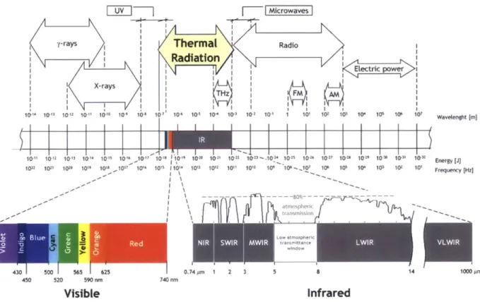
There exist several categorizations of the infrared (IR) spectrum [1,2, and others], but the one shown in Fig. 1.1 proves useful in that it is based on a combination of the atmospheric transmittance windows (i.e., the wavelengths regions in which the infrared radiation is best
__UV|
Mowavs
I II-rays y Thermal Radio
Radiation ectric powe X-rays 10 " 10 10, 10-" 101 10-' 10- 10, 106 10'1 Waveenght [m] ~I I P 10-11 0-0 10- 14 15 ,10 10-1 1 10 102 10 1024 104 10 '7 10' 10- 10 ' 1 avElnejrgy [ ] 1022 1o21 102 10" 1015 10 1 10 10 1 0 10-" 10l 10'n 10- 10 1 10- 10- 10" 10- 10- 10, Fruy [] 565 105 106740 lo 20 3 0 14 10F0uec [ 350 450 520 590 nm 740 nm Visible Infrared
Figure 1.1: The entire electromagnetic spectrum highlighting the infrared band located between the visible and radio waves. The Earth atmosphere's transmission bands in the infrared are also displayed. Adapted
from [3].
transmitted through the Earth's atmosphere), the detector materials used to build infrared sensors, and their main applications. According to
[1],
the JR band can be subdivided into five regions. The Near Infrared(NJR)
band is mostly used in fiber-optic telecommunication systems, where silica (SiO2)
provides a low attenuation loss medium for the near infrared.The Short Wave Infrared (SWIR) band allows for long-distance telecommunications using combinations of detector materials. The Medium Wavelength Infrared
(MWIR)
and the Long Wavelength Infrared(LWJR)
bands find applications in infrared thermography for military or civil applications, e.g. target signature identification, surveillance, non-destructive eval-Fation, etc. The MWIR band is preferred when inspecting high-temperature objects, whilethe LWIR band becomes more useful when working with near-room-temperature objects. Finally, the Very Long Wavelength Infrared (VLWIR) or Far Infrared (FIR) band is used in various kinds of spectroscopy, including astronomical spectroscopy.
1.1
The importance of infrared astronomy and the need
for space telescopes
The universe is in a state of constant expansion in which every wavelength traveling through it is stretched. In particular, much of the visible and ultraviolet light released billions of years ago has been stretched into the far-infrared region of the electromagnetic spectrum, a process known as redshift [4]. As a consequence, the very early steps of the universe can be studied by looking at very distant celestial bodies in the far-infrared and microwave regions of the electromagnetic spectrum (Fig. 1.2).
Many of the objects of interest to astronomers and astrophysicists, such as stars and planets in the early stages of formation and the powerful cores of active galaxies [6,7], emit most strongly in the infrared. Astronomical dust has been found in our solar system, around nearby stars with debris disks, in star formation regions and even in far-distant galaxies.
A diffuse glow of infrared radiation also permeates our own Milky Way galaxy. This is
generated by dust grains which absorb starlight and then reradiate that energy at infrared wavelengths [8-20].
It is in such cold and dusty environments that stellar formation processes often take place [21,22]. While planet formation processes are still under study (e.g., [23-25]), accord-ing to the solar nebula theory and planetesimal hypothesis [26], planets are formed duraccord-ing the collapse of a nebula into a thin disk of gas and dust. A protostar forms at the core, surrounded by a rotating protoplanetary disk. Through accretion, dust particles in the disk steadily accumulate mass to form ever-larger bodies. Local concentrations of mass known as planetesimals form and accelerate the accretion process by drawing in additional material by their gravitational attraction. These concentrations become ever denser until they collapse inward under gravity to form protoplanets.
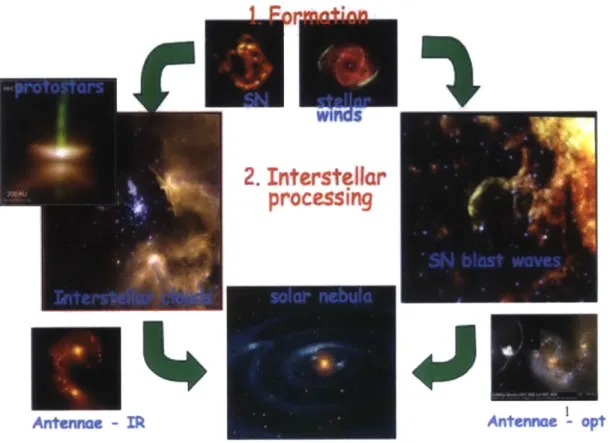
Dust is primarily formed in the quiescent outflows of asymptotic giant branch (AGB) stars I and in the stellar material explosively ejected in core-collapse supernovae (Fig. 1.3).
1In an AGB star, the core is so hot and its gravitational attraction on its outermost layers is so weak that those layers are expelled in a stellar wind. As each layer blows away, a hotter one is exposed and the stellar wind becomes stronger. These newly formed, fast winds slam into the old, slow winds that are still moving away from the star out in space. The process, thus, continues as more layers are exposed and ejected. These
Wavelength of radiation (m)
10-2 10-4 10-6 10-8 10-10 10-12 10-14 10-16 10-18,n 1000
CMB
C\J
100
E
(1
10
0.1
Star/
N?CX
co 0.1 CDBig Bang
0.01
AGN
c
0.001
LU1010
1012 1014 1016 1018 1020 1022 1024 1026Frequency of radiation (Hz)
After Hasinger, Nature 2000Figure 1.2: This figure captures the sense of where the energy can be found in the universe. Cosmic
Microwave Background (CMB) is a form of electromagnetic radiation left over from an early stage in the creation of the universe. It is not associated with any star, galaxy, or other object, but it shows itself as a faint background glow nearly exactly the same in all directions and is largely unpolarized. It represents the main contribution to the spectrum. The CMB is well characterized below 1 THz as a thermal black-body spectrum at a temperature of ~ 2.725 K, thus the spectrum peaks in the microwave range frequency of 160.2 GHz, corresponding to a 1.9 mm wavelength. Other forms of cosmic backgrounds are found in the infrared (CIB) and optical range (COB), which are due to stars and perhaps active galactic nuclei (AGN). The latter would be responsible for the cosmic background in the X-ray band (CXB), where the energy density is much lower. The error bars on the CMB curve are not shown as they are imperceptible on the figure presented; however, they are visible on the other curves, although they remain very small relative to other objects. Adapted
from [5].
Dust that forms in the explosive ejecta of a supernova is subjected to the harsh physical
envi-ronment of the young remnant, such as heating by X-rays and cosmic rays. The high velocities
of this material as it is injected into the interstellar medium (ISM) also lead to reverse shocks
that further process the dust grains. Standard models of interstellar dust assume a mixture
of silicates, graphite (or amorphous carbon), and polycyclic aromatic hydrocarbons (PAHs)
2.
Interstellar
processing
Antennwe - IR Antenne - opt
Figure 1.3: Dust forms in supernovae and in the outflows from stars, particularly evolved ones. From
these sources, through the action of winds and shocks in the interstellar and circumstellar medium, as well as transportation and diffusion processes generated by turbulence, dust becomes an important component of the interstellar clouds in which stars form. Dust can also find itself in the disk around a young star, where it can coalesce with other grains to form planetesimals, and ultimately planets such as Earth. Adapted from [27].
to simultaneously fit the average interstellar extinction, thermal infrared (IR) emission, and
elemental abundance constraints [29]. Furthermore, silicates and carbonaceous-type particles
have varying degrees of disorder, thus acting as an archaeological record of the environment
where they form and evolve [27,30].
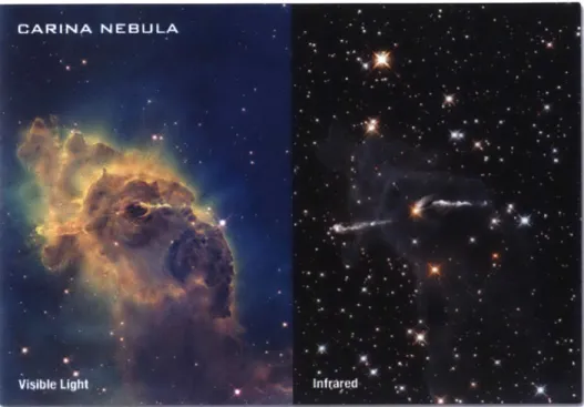
Dust shields sources from our view at optical wavelengths (Fig. 1.4), because dust
par-ticles are very effective at absorbing and scattering visible light, in accordance with
Kirch-hoff's law ("A good absorber is a good emitter") [31]. Extinction (scattering + absorption)
of visible light increases approximately linearly with decreasing wavelength [9]. As a
conse-quence, interstellar dust extinguishes blue light more efficiently than red light (Fig. 1.1), and
starlight transmitted through dust is therefore reddened, similarly to what molecular and
Figure 1.4: New stars forming in the Carina nebula can be seen in the infrared (right) behind the pillar of
gas and dust that appears in the visible-light image on the left. Credits: NASA, ESA, and the Hubble SM4
ERO Team.
dependent phenomenon, it was possible to infer that dust grains are small compared with optical wavelengths to be able to interact with the electromagnetic radiation and reprocess short-wavelength light to longer wavelengths [6]. Laboratory transmission measurements taken in the far-to-mid-infrared regime between 5.56 pm and 500 pm for SiO, grains [32,33] have allowed estimating the diameter of the particles (assumed to be spherical) to be 0.4 nm, comparable to that of the SiO4 tetrahedra found in [34] and equal to 0.5 nm. This grain size is the same order of magnitude as predicted by most models explaining interstellar dust grain size distribution [35, and references therein].
The uniqueness of infrared instruments lies therefore in the capability of infrared wave-lengths to detect and observe the emission of these dust particles, thereby enabling the observation of the above-mentioned phenomena otherwise impossible with visible light. As a consequence, infrared telescopes are crucial for understanding the distant young Universe.
NASA and the European Space Agency (ESA) have recognized the importance of infrared
ob-servations, as demonstrated by infrared missions such as NASA's Spitzer Space Telescope [36],
Tele-scope (JWST) [38], and ESA's Infrared Space Observatory (ISO) [39] and Herschel [40]. The
goal of these current and future missions is to explore a wide range of questions related to cosmology and provide the most detailed and highest quality far-infrared and submillimeter spectra of astrophysical sources yet achieved.
The importance of space-borne infrared telescopes resides also in the behavior of the Earth's atmosphere, which blocks many wavelengths of radiation and lets others through, due to its absorption bands (Fig. 1.1). For example, most infrared radiation is blocked out, except for a few narrow wavelength ranges that make it through to ground-based infrared telescopes. The atmosphere causes another problem: it itself radiates strongly in the infrared, often emitting more infrared radiation than the objects in space being observed. For these reasons, ground-based infrared observatories are usually located in deserts or plateaus, where the air is dry and the atmosphere relatively calm, or near the summits of high mountains, where it is possible to get above as much of the atmosphere as possible. Some examples in this category are the Atacama Large Millimeter Array (ALMA) [41], the Submillimeter Telescope (formerly know as the Heinrich Hertz Telescope) [42], the Submillimeter Array
(SMA) [43], the South Pole Telescope (SPT) [44], and the Keck Array [45]. Telescopes in
space, such as those mentioned above, and sometimes balloons flown to the high atmosphere (e.g., [46-49]) avoid all these problems and provide scientists with infrared spectra whose high (e.g.,
>
1200) resolution enables the exploration of the physical processes in the early universe (redshift z > 8).Chapter 2
Problem statement and objectives
2.1
Existing gaps and future needs
As described in Chapter 1, far-infrared and submillimeter (15 pm-1 mm, or equivalently 20 THz-300 GHz) spectroscopy provides a powerful tool to probe a wide range of environ-ments in the universe. In the past thirty years, many space-based observatories (e.g., [36,39, 40]) have opened the far-infrared window to the universe, revealing rich line and continuum spectra from objects ranging from interplanetary dust particles to major galactic mergers and young galaxies in the early universe. Discoveries made by these observatories have pro-vided unique insights into physical processes leading to the evolution of the universe and its contents. This information is encoded in a wide range of molecular lines and fine-structure lines. The fine-structure lines of abundant elements such as carbon, nitrogen, and oxygen are seen in the 50-200-ym rest frame, but with a spectrometer operating in the far-JR/sub-mm they can be observed in star-forming galaxies out to redshifts z > 5. This therefore enables
tracing the obscure star formation and AGN activity into the high-redshift (and thus older) universe. Nonetheless, a number of questions remain to be answered. For example:
. What are the first galaxies? Where did they form?
. When and how did reionization occur? What sources caused it? . How did the heavy elements form?
* What physical processes determine galaxy formation?
. How does the environment affect star formation and vice versa? . How do protoplanetary systems form?
. What are the life cycles of gas and dust?
. How do planets form? How are habitable zones established?
The National Academies' 2010 Decadal Survey report, New Worlds, New Horizons in
As-tronomy and Astrophysics [50], recommended a suite of missions and technology development
programs aimed to further our understanding in the following three areas: . Cosmic dawn: searching for the first stars, galaxies, and black holes . New worlds: seeking nearby, habitable planets
. Physics of the universe: understanding scientific principles
Some of the specific missions that will probe in more detail all of the above-mentioned processes might be the Wide-Field InfraRed Survey Telescope (WFIRST) [51], NASA's Ex-plorer Program [52], the US contribution to the Japanese Aerospace Exploration Agency
(JAXA) SPace Infrared telescope for Cosmology and Astrophysics (SPICA) mission [53],
as well as technology development programs for ultraviolet-optical-infrared (UVOIR) space capabilities and for studying the Epoch of Inflation. These far-IR missions will require tech-nology development in the following areas: large, cryogenic far-IR telescopes; large-format, low-noise, as well as ultra-low-noise far-IR direct detectors; photon-counting far-IR detector arrays; interferometry for far-IR telescopes; and high-performance sub-kelvin coolers. Ta-ble 2.1 illustrates the requirements for each of these areas and their potential benefits to the astrophysics community, NASA, and the aerospace industry [54].
Table 2.1: Summary of astrophysics technology needs for the 2015-2035 frame and their benefits (Adapted from [54])
Photon-Large-format, Ultra-low-noise, Interferometry High- counting Technology Large, telescopes low-noise, far-IR far-IR direct for far-IR sub-kelvin far-IR
direct detectors detectors telescopes coolersdetector
arrays
Optimized for the very
Provide light Optimized for the very Opt o Poi spta
gathrin poer t lo phtonlow photon Provide spatial
gathering power to low photon backgrounds present resolution to see
see the faintest backgrounds present in space for the most detail and Be compact,
targets. Provide in space. Arrays low-power,
spatial resolution containing up to tens spectroscopy. Arrays reduce source and
to see the most of thousands of pixels confusion. lightweight to
detail and reduce to take full advantage thousands of pixels to Structurally provide
source confusion. source confusion. of ofatheffocal planthe focal plane cooling for High quantum To achieve the available on large the spectral free-flying space flight efficiency and
Requirements information content interferometric conditions fast response
ultiatecryoeni telscoes. available. Detector telescope systems
sensitivity, their Detector sensitivity svity reqeto reqedor which require time. emission must be required to achieve aehiev e fr-futre o s temperatures
minimized, with background-limited achieve far-future missions of operation
operating performance, using background-limited in far-JR. in the order of performance, using Telescopes tens of
temperatures as direct (incoherent) direct (incoherent) operated attesf
low as 4 K. detectors to avoid millikelvin.
. . detectors to avoid temperatures as Collecting areas on quantum-limited qunu-imtdlw.s4K
2 ~quantum-limited low as 4 K.
the order of 50 m2
. sensitivity. sensitivity.
Missions will
Provide spatial Sensitivity reduces operate ~ 100
resolution and observing times from 40-m baselines times faster.
sensitivity many hours to a few sevitees required to provide Enable the Distant
necessary to follow minutes (~ 100 times oeng ties o the spatial use of far-IR missions beyond many hours to a few
up on discoveries improvement). Array minutes ( 100 times resolution needed telescopes in the Zodiacal Benefits with current format increases areal improvement) to follow up on the next dust
generation of space coverage by 10 to 100 m veal discoveries with decade and of cloud [55,56]
telescopes. times. Overall inse can current and next certain X-ray will observe
Low-cost, mapping speed can thousands.generation of space detectors. > 10 times
lightweight, increase by factors of telescopes. faster even in
cryogenic optics. thousands. imaging
applications.
The ability to fully explore this rich spectral region has been limited by the size, mass, power constraints, limitations in sensitivity, and cost of the cryogenic spectrometers required to carry out these measurements. The work presented in this thesis specifically addresses the need for integrated, ultra-low-noise, far-IR, direct-detection spectrometers, whose specific requirements are expected to be satisfied by Technology Readiness Level (TRL) 6-level technologies in the 2015-2035 frame [57]. These are shown in Table 2.2 and compared against the current state of the art.
Table 2.2: Summary of requirements for far-JR spectrometers and detector arrays and comparison with
current state of the art [57]
Metric State of the art Requirements
Wavelength, A 250-700 pm 220-2000 1m
Noise Equivalent Power, NEP 10-18 W/Hz < 10-20 W/Hz
Resolving power, R > 100 > 1200
Detective quantum efficiency, DQE ~ 15% > 90%
Temperature, T < 1 K < 0.05 K
Time constant, T 100 ms < 10 ms
In Table 2.2, the required wavelength range is dictated by the type of science discussed in Chapter 1 and needed to answer the cosmological questions posed at the beginning of this section: high-redshift galaxy evolution, physical conditions of the interstellar medium in normal and star-forming galaxies across cosmic time, study of elemental abundances, etc. [50].
The Noise Equivalent Power (NEP) is a measure of the sensitivity of a photodetector or detector system and is defined as the signal power that gives a signal-to-noise ratio (SNR) of 1 in an output bandwidth Af = 1 Hz [58]. An output bandwidth of 1 Hz is equivalent to half a second of integration time, t = 1/(2Af) = 0.5 s, from the Nyquist-Shannon sampling
theorem. A smaller NEP corresponds to a more sensitive detector. For example, a detector with a NEP of 10-1' W/ Hz can detect a signal power of 1 attowatt (aW) with a SNR of
1 after one half second of averaging. The SNR improves as the square root of the averaging
time, and hence the SNR in this example can be improved to 10 by averaging for 50 seconds. The NEP values shown in Table 2.2 are determined by the requirement to be background-limited and not detector-background-limited, that is, the noise thermally generated by the detectors must be lower than that presented by the astronomically observed background flux. This is defined
as background-limited performance (BLIP). Because the far-IR/sub-mm wavelength range is mainly characterized by the cosmic microwave background (CMB, see Fig. 1.2) with a NEP on the order of 10-18 W/v'lz
[59],
the detectors' BLIP is required to be lower than this.The resolving power, R, of a spectrometer is a measure of its ability to resolve spectral features and is defined as R = A/AA, where A A is the smallest difference in wavelengths that can be distinguished at a wavelength A. For example, with a resolving power of 1000 at a wavelength of 600 pm, a spectrometer can resolve features 0.6 pm apart. A resolving power greater than 1200, as shown in Table 2.2, is again imposed by the type of science previously described, and in particular by the need of resolving exoplanets around stars.
The quantum efficiency (QE) is the flux absorbed in the detector divided by the total flux incident on its surface and is a measure of a device's electrical sensitivity to light. Since the energy of a photon is inversely proportional to its wavelength, the QE is often measured over a range of different wavelengths to characterize a device's efficiency at each photon energy level. This definition of quantum efficiency, however, refers only to the fraction of incoming photons converted into a signal in the first stage of a detector. In fact, in an ideal scenario, the signal-to-noise ratio attained in a measurement is controlled entirely by the number of photons absorbed in the first stage. However, additional steps in the detection process can degrade the information present in the photon stream absorbed by the detector, either by losing signal or by adding noise. The detective quantum efficiency (DQE) describes this degradation in terms of the square of the ratio of the actually observed signal-to-noise ratio to the signal-to-noise ratio of the incoming photon stream [60, Ch. 1].
Cryogenic temperatures are necessary to achieve background-limited performance by re-ducing the telescope and instrument thermally-generated noise. For example, away from the galactic plane, the background would be determined by the CMB, associated with a tem-perature of ~ 2.725 K, while in the galactic plane it would be dominated by the infrared emission of dust, as previously discussed (see Fig. 1.2). Cryogenic temperatures also allow for the use of superconducting materials with critical temperatures below 13 K (e.g., niobium and molybdenum nitride) and which are practical from an engineering standpoint.
Broadband Delay 2-D Feed Absorber Filter Bank Filter MKID
Antenna Network & Detectors Bank Detector
2ko ~i+1
_-C - ~Prirmary.. --
24 4 '' ik-i Beam -_
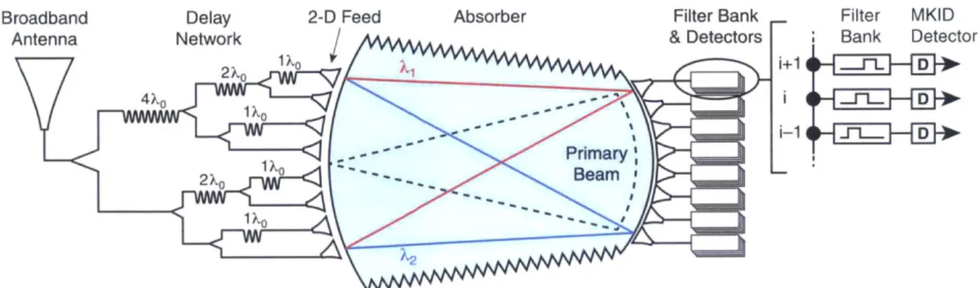
Figure 2.1: Layout of the p-Spec module. The radiation collected by the telescope is coupled into the
instrument using a broadband antenna (left). It is then transmitted through a low-loss superconducting transmission line to a divider and a phase delay network, which creates a retardation across the input to the multimode region (in light blue). The feed horns will radiate a converging circular wave, which will concentrate the power along the focal surface, with different wavelengths at different locations. The outputs are connected to a bank of order-sorting filters to disentangle the various orders [61].
Finally, the time constant, T, represents the minimum interval of time over which the
detector can distinguish changes in the photon arrival rate. A smaller time constant implies
a detector with a faster response and ability to capture variations in the photon flux dynamics,
as long as it does not impact the spacecraft performance (e.g., data rate, avionics, etc.).
2.2
Filling the gaps with Micro-Spec
To attain the goals outlined in Table 2.2 and fill in the gaps in the current state of the art,
a high-performance integrated spectrometer module, ti-Spec, is being developed for use on
space-borne telescopes such as SPICA [53] or high-altitude balloon-borne far-IR payloads. More in detail (Fig. 2.1), p-Spec operates in the 450-1000-pm (300-650-GHz) spectral range. In p-Spec, the incoming radiation collected by the telescope is coupled to the
spectrom-eter through a broadband dual-slot antenna used in conjunction with a hyper-hemispherical
silicon lens and directed to a series of power splitters and a delay network made of
super-conducting microstrip transmission lines. The delay network creates a retardation across
the input to a planar waveguide multimode region which has two internal phased arrays,
Ab-sorber structures lining the multimode region terminate the power emitted into large angles or reflected from the receiver antenna array. The radiation is coupled to the multimode region via an array of planar feed structures, which concentrate the light along the focal surface with different wavelengths at different locations. The outputs are connected to a bank of order-sorting filters which terminate the power in an array of microwave kinetic in-ductance detectors (MKIDs) for detection. Read-out is done using conventional homodyne techniques and commercial field-programmable gate array (FPGA)-based software-defined radios (SDRs) [62,63]. p-Spec can be used in a modular fashion by assembling several iden-tical spectrometers to perform multi-object spectrography.
One of the techniques adopted for p-Spec is the use of monocrystalline silicon combined with superconducting materials, which reduce losses to a minimum. This provides a necessary prerequisite to attain the required background-limited sensitivity (NEP < 10-20 W/V/fHiZ) at a resolution 1 > 1200, thus potentially making p-Spec four orders of magnitude more sensitive than its most capable predecessors (Fig. 2.2).
10-15 GR EAT/$OFIA 1 FIFI LS/SOFIA - CASIM[R/' 10-HIFV/ PACS Herschel Hersche
10 LA\ ALMA c --10-21 100 200 500 1000
Wavelength (pm)
Air
Ground plane
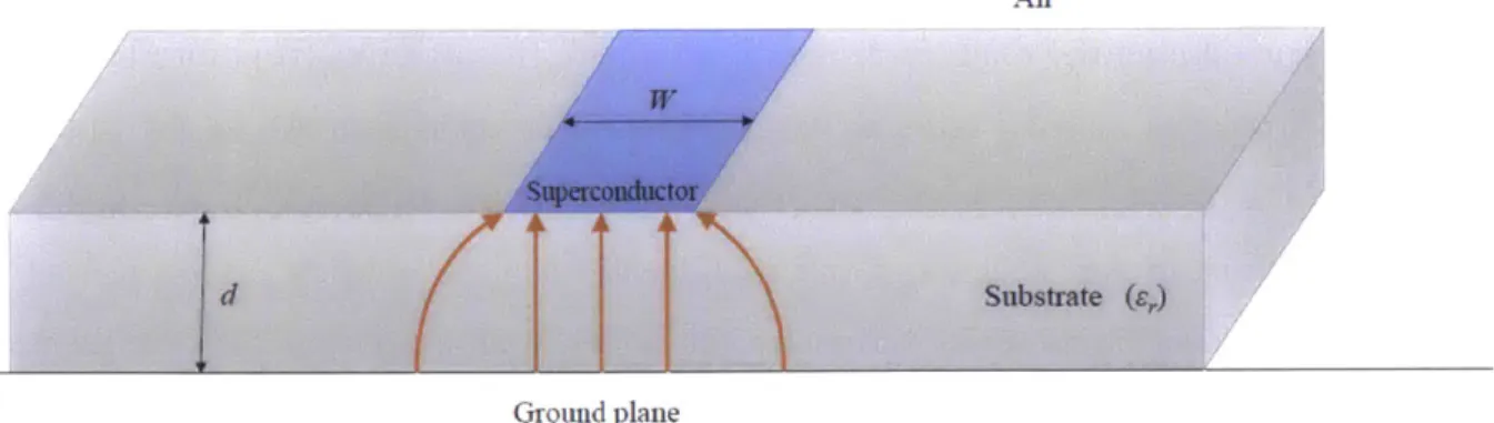
Figure 2.3: Geometry of a microstrip transmission line. In orange are the electric field lines indicating their
dominant modal symmetry.
The instrument is integrated on a 100-mm-diameter silicon chip. This size reduction is achieved through the use of single-mode microstrip transmission lines, which can compactly be folded on the silicon wafer and reduce the required physical line length by a factor of
the material's effective refractive index. Specifically, a transmission line is a distributed-parameter network whose dimensions are on the order of microwave or submillimeter wave-lengths. Because of this, the phase of a voltage or current varies greatly over the physical extent of the transmission line. This is opposed to the behavior at lower frequencies, where the wavelengths are large enough that there is insignificant phase variation across the dimen-sion of the electrical component (a lumped-element circuit). At higher frequencies, instead, the wavelengths are much shorter than the dimensions of the device and Maxwell's equations simplify to the geometrical optics regime [65]. A microstrip line is a type of planar trans-mission line, whose geometry can be seen in Fig. 2.3. A conductor of width W is printed on a grounded dielectric substrate of thickness d and relative permittivity Er. This structure can be fabricated by photolithographic processes and integrated with other active or passive microwave devices. The material's effective dielectric function, Er,eff, is a weighted combi-nation of the dielectric functions of both the substrate and the air around the structure: Er,eff qf Er(substrate) + (1 - q,) E,(air), where q, represents the dielectric filling fraction of
the substrate. The effective dielectric function can be interpreted as the dielectric function of a homogeneous material that replaces both the air and the substrate [65]. The dielectric filling fraction is defined as q, = (F + 1)/2, where F depends only on the substrate thickness and the superconductor width, but not on the substrate dielectric function, Er,eff [66].
As for the choice of the instrument operational spectral range, apart from being of scien-tific interest for all of the reasons described in Chapter 1, it also lies below the gap frequency of the superconductors that are being considered for the development of the transmission lines. These include niobium (Nb), niobium-titanium nitride (NbTiN), and molybdenum nitride (MoN), with critical temperatures of 9.3 K, 17.1 K, and 5 to 12 K, respectively. In particular, unless a low-loss superconductor with a gap larger than NbTiN becomes available, the technology is confined to wavelengths A > 250 1m.
The predicted sensitivity of the instrument can be achieved by employing an array of low-noise (NEP < 10-2 0W/Hz) direct (incoherent) detectors and reducing the stray light
falling on the detectors. Direct detectors are promising because they are not affected by quantum noise caused by spontaneous photon emission. In our case, because the infrared thermal background is their dominant source of noise, they are background-limited and photon counting is possible at least in principle
[67].
In addition, superconducting materials exhibit extremely low losses below their critical temperature, and thus represent a crucial element for this type of technology, as explained above.The reduction in stray light is accomplished by coupling the spectrum efficiently to the optical system via a hyperhemispherical lens (Fig. 2.1). Since the only input to the in-strument is through its broadband antenna, it provides unique protection of the low-NEP detectors from their surrounding environment. In other words, ti-Spec will be an integrated spectrometer as it has this feature designed in from its conception, thereby overcoming the challenge of controlling undesired radiation in this type of sensitive detectors.
Finally, augmenting the number of p-Spec modules will allow for multi-object spec-troscopy as each module can independently analyze the light coming from different objects. As for the maximum number of modules that can be accommodated, the limiting factor is the power constraints as well as the efficiency and volume available for the electronics, both warm and cold. The warm electronics requires further study as no flightworthy electron-ics systems for the instrument detectors has been built. High electron mobility transistor (HEMT) amplifiers for use in space can be produced with noise temperature of 3 K for about 2 mW of power dissipation at 4 K [68-70]. With 1000 resonators per GHz, this would be
sufficient for a few thousand detectors. In order to increase the number of detectors, studies will be necessary to explore alternatives for minimizing power dissipation. This, however, is beyond the scope of the work described here and can be addressed when more information becomes available on the specific type of mission that will require to fly the p-Spec technology (e.g., a space telescope or an atmospheric balloon).
2.3
Thesis objectives
Figure 2.4 below is a simplified representation of Fig. 2.1, which shows the different subsys-tems of li-Spec. The specific contributions of this thesis work look at the delay network, the multimode region, and the detector subsystems.
INPUT Broadband Delay network Multimode -- DttrsUTT
INPUT antenna (Transmission line) region _ 1 eetr.sOTU
Figure 2.4: Block diagram of the p-Spec module. The filter banks have been omitted in the Detectors box
for clarity. The red box identifies the three subsystems object of this thesis work.
The primary technical questions which must be answered to enable the p-Spec technology are the following:
1. What is the dielectric loss in the inicrostrip transmission lines over the required spectral
range (300-650 GHz)? How does it differ for amorphous and monocrystalline materials? Which materials would be best suited to maximize the coupling efficiency in the system? 2. Does there exist a feasible design of a spectrometer that meets the requirements in Table 2.2? What are the trade-offs involved in this design? How can the instrument performance be optimized in terms of coupling efficiency and spectral purity?
3. What are the propagation properties of the microstrip transmission lines made of
super-conductors such as molybdenum nitride and niobium? These parameters are needed for the design of the detectors and read-out system. Can the determination and accuracy of these parameters be improved, and how?
The main objective of this thesis is to explore the feasibility of this new technology concept and develop the necessary tools to answer these questions. The approach followed is summarized below.
1. To study the loss of dielectric materials to be used as substrates in the microstrip
transmission lines, analytical models and numerical algorithms have been developed to extract the dielectric function of these materials from laboratory transmission data as a function of frequency. The final result is a database of infrared dielectric properties of silicon-based materials with applications in spectrometry and detectors development, such as silicon nitride, silicon oxide, and single-crystal silicon.
2. To find feasible designs for an ultracompact (10-cm2) spectrometer that satisfy the
requirements in Table 2.2, an optical design methodology has been developed for the spectrometer diffractive region over the 450-1000-pm wavelength range. This method-ology is used to explore the design space and find optimal solutions that simultaneously maximize the instrument throughput and minimize the phase error on the focal plane. Several designs have been found and the following five case studies are examined in detail:
. A proof of concept of a low-resolution (R = 65), first-order design to be used to build and test a spectrometer prototype
. Four medium/high-resolution (R > 250), higher-order designs optimized to yield
a nearly 100% throughput and maximize the focal plane utilization for potential use on flight missions
3. To study the properties of the superconducting materials employed in the transmission
lines and detectors, analysis and calibration techniques have been developed for su-perconducting resonators commonly employed in MKIDs, with particular attention to what causes performance degradation (e.g., two-level systems mentioned in Chapter 5).
2.4
Thesis outline
The presentation of this thesis will guide the reader through each of the three subsystems illustrated in Fig. 2.4. Each chapter will be articulated as follows: question(s) to be answered, brief review of the state of the art, summary of specific current technology gaps, description of the found solution with details of the adopted methodology, and review of the results.
Chapter 3 will address Question 1 by describing the models developed and used to extract the dielectric properties of two amorphous materials, namely, silicon nitride and silicon oxide. Their derived loss is compared to that of single-crystal silicon data from the literature to show that low-loss monocrystalline materials will be necessary in the transmission lines.
Chapter 4 will address Question 2 and will describe in detail the design of the ti-Spec multimode region with all the trade-offs involved. A discussion of the numerical methods used will also accompany the discussion as a complement to the challenges encountered to solve large complex systems of equations.
Chapter 5 will address Question 3 by presenting novel analysis and calibration techniques for superconducting resonators that compose the p-Spec detectors. A phenomenological model is first presented for the computation of the resonators' quality factors and central frequencies. An ABCD-matrix approach is then proposed to validate the phenomenological model and extract more detailed information on the resonators' internal structure.
Finally, Chapter 6 will summarize the main findings of this thesis work and discuss possibilities for future work.
Chapter 3
p-Spec transmission lines: materials
characterization
Question 1: What is the dielectric loss in the microstrip transmission lines over the required spectral range (300-650 GHz)? How does it differ for amorphous and monocrystalline materials? Which materials would be best suited to maxi-mize the coupling efficiency in the system?
The p-Spec power divider, delay network, and detectors are all realized through microstrip transmission lines (Fig. 2.4). As shown in Section 2.2, these are generally characterized by a dielectric substrate holding a thin layer of conducting material etched in the substrate sur-face through photolithographic processes. To reduce materials losses in such high-sensitivity systems, it is crucial to employ superconducting materials and single-crystal dielectric sub-strates.
In superconductors, electrical currents can flow without resistance below a characteristic critical temperature, thereby minimizing losses in the energy through the material. Examples of superconductors are aluminum, molybdenum, niobium, titanium, mercury, zinc, or alloys such as niobium-titanium, molybdenum-nitride, and magnesium diboride, each character-ized by its own critical temperature usually below 40 K. Niobium, niobium-titanium-nitride, and molybdenum nitride have been chosen as possible candidates for p-Spec, because their conduction bands lie within the spectral range of interest, their critical temperatures are
attainable without requiring sophisticated cooling systems, and they can be handled safely. In single-crystal dielectrics, the crystal lattice of the entire solid is continuous and without grain boundaries. The grain boundaries are defects in the crystal structure which tend to decrease the electrical and thermal conductivity of the material and are important to many of the mechanisms of creep. The absence of similar defects confers monocrystalline materials unique mechanical, optical, and electrical properties, making them an important resource for many industrial applications, especially in electronics and optics. In addition, they are suited to reach optimal sensitivities because they reduce losses and noise associated with two-level systems typically found in amorphous (non-crystalline) materials (see Sec. 5.1).
This chapter will address the characterization of the dielectric properties of amorphous silicon compounds through the derivation of their complex dielectric functions over the fre-quency range of interest (the far-infrared, in this case) from measured transmission data. These complex dielectric functions will then be compared with those of single-crystal silicon samples that were previously analyzed by the author [71, 72] or that can be found in the literature [73, 74]. This will serve as a comparison of materials with distinct properties and applications, and it will show the superiority of monocrystalline silicon.
To perform this study, the transmission of these materials samples was measured in the infrared through Fourier Transform Spectroscopy (FTS). Appropriate mathematical models were then used to fit these data and extract the materials' complex dielectric functions. The mathematical models and numerical methods employed to analyze the transmission measurements have been developed by the author and discussed in [32,33,75,76]. The next two sections report specifically on the characterization of amorphous silicon-nitride samples, as described in [75] (Sec. 3.2), and silicon-oxide membranes (Sec. 3.3). The characterization of the superconducting materials is addressed in detail in Chapter 5, since it requires different measurement approaches and analysis techniques.
3.1
The complex dielectric function
The electromagnetic response of a material as a function of frequency, W, is represented by its relative permittivity, Er(W) = E'(W) + i ','(w), defined as the ratio of the material's complex
absolute permittivity (or complex dielectric function), &(w), to the vacuum permittivity, E,.
From a physical perspective, the absolute permittivity defines the material's polarizability (i.e., the average dipole moment per unit volume) relative to the incident electric field. Its real part determines the phase velocity in the material, while its imaginary part the attenuation of electromagnetic waves passing through the medium.
The real and imaginary components of the complex refractive index, N = n + itt, can readily be derived from those of the complex dielectric function as follows:
n =
\
2 ' 2 ' (3.1)assuming the material to be nonmagnetic (P = p").
H. A. Lorentz developed a classical theory for the complex dielectric function, in which electrons and ions are treated as harmonic oscillators subject to an elastic force, a damping force, and the driving force of the applied electromagnetic field. The model assumes the atoms to be a collection of identical, independent, isotropic, harmonic oscillators with a certain mass and charge. The equation of motion of these oscillators can therefore be expressed as a second-order differential equation. The oscillatory solution, with the same frequency as the driving field, can readily be related to the material's polarizability, and thus to the complex dielectric function. A more in-depth description of this theory is provided in
[6],
where other models are also discussed, such as the Drude model for free-electron metals or the Debye relaxation model for polarizing matter with permanent (as opposed to induced) electric dipoles. More models exist in the literature [77,78], some of which will be described in the next sections.3.2
Analysis of the dielectric properties of silicon
ni-tride thin films
The study of the infrared dielectric properties of silicon nitride thin films was presented by the author and collaborators in
[75].
It is reported in the remainder of this section as foundin this reference, with minor edits to improve clarity.
"Silicon nitride films are amorphous, highly absorbing in the mid-IR [79], and their gen-eral properties are functions of composition [80,81]. Silicon nitride thin films are commonly employed in the microfabrication of structures requiring mechanical support, thermal isola-tion, and low-loss microwave signal propagation [82-85]. The optical tests were performed on samples having membrane thicknesses of 0.5 and 2.3 pm with an uncertainty of 3%.
The dielectric response is represented as a function of frequency, W, by the classical Maxwell-Helmholtz-Drude dispersion model [77]:
M A. C2
E" + 2 _W Ti 32
j=1 Ti w~w 32
where M is the number of oscillators and Er = E' i 'c is a complex function of (5M + 2) degrees of freedom, which are as follows: the contribution to the relative permittivity EO =
EM+1 of higher lying transitions, the difference in relative complex dielectric constant between
adjacent oscillators A E = (E - Ej+l which serves as a measure of the oscillator strength, the
oscillator resonance frequency wr, and the effective Lorentzian damping coefficient F', for
j
= 1, ... , M. For the silicon nitride films analyzed, the following functional form was usedto specify the damping:
F'(w) = Fj exp -ozj Ti (3.3)
where aj allows interpolation between Lorentzian (aj = 0) and Gaussian wings (a3 > 0)
sim-ilar to the approach in [86]. The form indicated above enables a more accurate representation of relatively strong oscillator features.
The impedance contrast between free space and the thin-film sample forms a Fabry-Perot resonator. The observed transmission can be modeled [87] as a function of the dielectric response [Eq. (3.2)], thickness, and wavenumber. The dielectric parameters were solved by means of a non-linear least-squares fit of the transmission equation to the laboratory FTS data. Specifically, a sequential quadratic programming (SQP) method with computation of
0.8-C
0.6-0
Cn Measured
- ---. Model
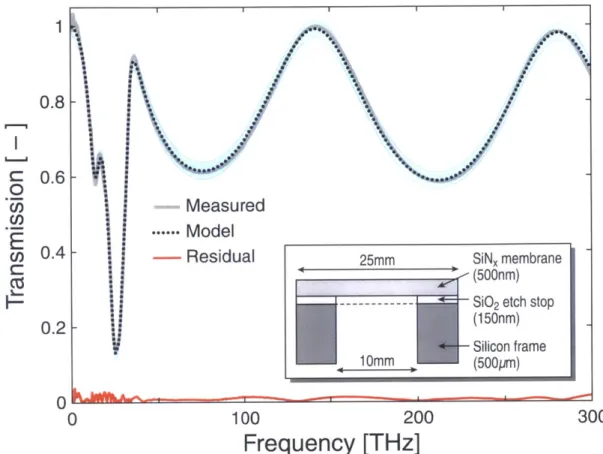
C 0.4- - Residual 25mm SiNx membrane
__ (500nm)
--- SiO2 etch stop
0.2- (150nm)
U
10mm Silicon frame 10m , (500pm) 0 0 100 200 300Frequency [THz]
Figure 3.1: Room-temperature transmission of a silicon nitride sample 0.5 pm thick: measured (grey),
model (black dotted), and residual (red). The shaded band's width delimits the estimated 3- measurement uncertainty. A 30 GHz (1 cim-') resolution is employed for the measurement. The insert depicts the geometry of the SiN, membrane and micro-machined silicon frame. Adapted from [75].
the Jacobian and Hessian matrices [88, 89] was implemented. The merit function, x2,was
used in a constrained minimization over frequency as follows:
N -1-2
min X - min T(Er (Lu), h) - TFTSk (3.4)
DOF DOF
where N is the number of data points, T the modeled transmittance, TFTS the measured
transmittance data, and h is the measured sample thickness. We are guided by the
Kramers-Kronig relations in defining constraints for a passive material:
KAjj
> lj+1i, <'! > 0 and Er(0) = El [90].1 [The Kramers-Kronig relations ensure causality, so that the light cannot be reflected or absorbed by a system before the arrival of the primary light wave.] Foraccurate parameter determination the sample should have uniform thickness, be adequately
1The transmission cannot be zero, because if it were the field must vanish throughout the space. This would not be possible when a miultilayered stack, as is the case here, is illuminated by a plane wave [91].
![Table 2.1: Summary of astrophysics technology needs for the 2015-2035 frame and their benefits (Adapted from [54])](https://thumb-eu.123doks.com/thumbv2/123doknet/14744691.577788/23.1187.130.1097.117.805/table-summary-astrophysics-technology-needs-frame-benefits-adapted.webp)
![Table 2.2: Summary of requirements for far-JR spectrometers and detector arrays and comparison with current state of the art [57]](https://thumb-eu.123doks.com/thumbv2/123doknet/14744691.577788/24.918.167.757.387.560/table-summary-requirements-spectrometers-detector-arrays-comparison-current.webp)
![Figure 2.2: Sensitivities of state-of-the-art ground and space telescopes. Adapted from [64].](https://thumb-eu.123doks.com/thumbv2/123doknet/14744691.577788/27.918.199.689.580.1015/figure-sensitivities-state-art-ground-space-telescopes-adapted.webp)