UNIVERSITÉ DE MONTRÉAL
SIX-PORT TECHNOLOGY FOR MILLIMETER-WAVE MIMO SYSTEMS
TAO JIANG
DÉPARTEMENT DE GÉNIE ÉLECTRIQUE ÉCOLE POLYTECHNIQUE DE MONTRÉAL
MÉMOIRE PRÉSENTÉ EN VUE DE L’OBTENTION DU DIPLÔME DE MAÎTRISE ÈS SCIENCES APPLIQUÉES
(GÉNIE ÉLECTRIQUE) MAI 2014
UNIVERSITÉ DE MONTRÉAL
ÉCOLE POLYTECHNIQUE DE MONTRÉAL
Ce mémoire intitulé:
SIX-PORT TECHNOLOGY FOR MILLIMETER-WAVE MIMO SYSTEMS
présenté par : JIANG Tao
en vue de l’obtention du diplôme de : Maîtrise ès sciences appliquées a été dûment accepté par le jury d’examen constitué de :
M. CARDINAL Christian, Ph.D., président
M. WU Ke, Ph.D., membre et directeur de recherche
M. TATU Serioja, Ph.D., membre et codirecteur de recherche M. BOUTAYEB Halim, Ph.D., membre
DEDICATION
ACKNOWLEDGE
First of all, I would like to express my gratitude to my supervisor Dr. Ke Wu and co-supervisor Dr. Serioja Tatu, who gave me the opportunity to pursue the master studies at École Polytechnique de Montréal. Their passion for research, their patience, and their innovative ideas have impressed me and driven me to explore new space in our field and accomplish this thesis.
I would also like to thank all the personnels at the Poly-Grames Research Center, in particular the technician team including Mr. Jules Gauthier, Mr. Steve Dubé, Mr. Maxime Thibault, and Mr. Traian Antonescu, for their great work in circuit fabrication and measurement. My gratitude is extended to Mrs. Ginette Desparois and Mrs. Elena Pavlov for their administrative work and to Mr. Jean-Sébastien Décarie for his IT support.
I am indebted to all my student colleagues for their professional advice, in particular Ya Deng, Wei Wang, Jiudong Wu, Kuangda Wang, Yangping Zhao,Zoé-Lise Deck-Léger, Sulav Adhikari, and Nasser Ghassemi. It is a great pleasure to study and work with them.
I appriciate all the advice and help from my friends. They gave me the feeling of being at home when I was staying in Montrel.
I would like to thank all the jury members for their time and efforts in reviewing my thesis and providing me valuable comments.
Last but not least, I would like to thank my parents, who gave me the birth and brought me up. They always support me, listen to me and love me. I would like to express my deepest gratitude to the special and beautiful girl Katherine Li, for her endless love, encouragement and support.
RÉSUMÉ
Les taux de transmission des systèmes de communication sans-fil modernes augmentent. De nouvelles bandes de fréquences et de nouvelles technologies sont exploitées pour supporter de hauts taux de transmission. La bande d’ondes millimétriques est une bonne candidate pour supporter des taux de transmission de l’ordre des Gbps. De plus, la technologie à entrées/sorties multiples (MIMO) ouvre la porte à des systèmes de communication à bas coût à haut taux de transmission.
Le récepteur hétérodyne standard est utilisé dans plusieurs systèmes de communication, puisqu’il présente une grande sélectivité et une grande sensibilité. Par contre, le récepteur à conversion directe permet un meilleur niveau d’intégration en diminuant le nombre de composants des circuits. Parmi les récepteurs à conversion directe, ceux à six ports ont un circuit passif qui sert d’interferomètre. La diversité additionnelle est produite par les sorties en quadrature, qui sont des combinaisons linéaires du signal d’entrée et du signal de référence. Les guides d’onde intégrés au substrat (SIW) peuvent être facilement intégrés à des circuits planaires. La conception est simplifiée puisqu’il existe des méthodes de conception de guides d’ondes traditionnels. Un système MIMO à six ports de type SIW est présenté dans cette dissertation.
Premièrement, un diviseur de puissance et un coupleur hybride de type SIW sont présentés. L’implémentation de ces circuits, basée sur les règles de conception des structures SIW, est réalisée une bande de fréquence d’intérêt. Plusieurs paramètres critiques peuvent être manipulés pour contrôler les performances du diviseur de puissance et du coupleur hybride. Une transition de la structure SIW à la ligne micro-ruban est conçue pour permettre des mesures. Les résultats de simulation du circuit démontrent que celui-ci offre une bonne performance.
Deuxièmement, à partir du diviseur de puissance et du coupleur hybride, le circuit à six ports est présenté. Trois types d’architechtures sont comparées, et l’une d’elles est choisie pour le système de démonstration. Les résultats de simulation et les résultats expérimentaux concordent, et guarantissent une bonne performance du circuit proposé et du système de communication sans-fil dans lequel le circuit est intégré.
Finalement, le système de 2 2 ports est présenté. Il n’y a pas de couplage réciproque entre les deux récepteurs lorsque le critère de propagation de Rayleigh dans la ligne de visée est respecté.
Les multiples ports de sortie en quadrature du circuit à six ports garantissent que la performance du système MIMO sera acceptable lorsque des paramètres sont modifiés. Ceci peut être prouvé par le taux d’erreurs sur les bits dans différents cas.
ABSTRACT
Presently, the data rates in modern wireless communication systems are becoming higher and higher and new frequency bands and technologies are being exploited in support of high data transmissions. The millimeter-wave band is a candidate of choice to support Gbps data transmission. In addition, Multiple-Input Multiple-Output (MIMO) technology will open the way for low-cost reliable communication systems that require even higher data rates.
While the conventional heterodyne receiver has been widely applied in many kinds of communication systems due to its high selectivity and sensitivity, the direct-conversion receiver allows higher-level circuit integration by reducing the number of circuit components. Among these direct-conversion receivers, six-port scheme presents a passive circuit that acts as an interferometer. The additional diversity is produced by the quadrature outputs of the six-port circuit that are linear combinations of the unknown input signal and the reference signal. Substrate integrated waveguide (SIW) can be integrated with planar circuits easily. The design procedure is obviously simplified as a result of the existing typical design methods for the rectangular waveguide. Based on the above techniques and discussions, the millimeter-wave MIMO system based on SIW six-port circuit is presented in this dissertation.
First, the SIW power divider and hybrid coupler are presented. The implementation of those circuits is based on the SIW design rules, according to the working frequency band of interest. Several critical parameters can be manipulated to control performances of the SIW power divider and hybrid coupler. An SIW to microstrip line transition is designed for measurement purposes. Simulation results of the circuits show good performances.
Second, based on the studied and designed SIW power divider and hybrid coupler, the six-port circuit is presented. Three types of six-port architecture are compared, with one of them chosen to work in our millimeter-wave MIMO system demonstration. Simulation and measurement results agree well and guarantee a good performance of the proposed circuit itself and wireless high-speed communication system in which the circuit is embedded.
Finally, the 2 2 millimeter-wave MIMO system is presented. There will be no crosstalk between two receiver array responses when the line-of-sight (LoS) propagation Rayleigh criterion is satisfied. Multiple quadrature outputs of the six-port circuits ensure that the performance of the
MIMO system will stay acceptable when some parameters are changed. This can be proven by the bit error rates (BER) in different cases.
TABLE OF CONTENTS
DEDICATION.... ... III ACKNOWLEDGE ... IV RÉSUMÉ... ... V ABSTRACT... ...VII TABLE OF CONTENTS ... IX LIST OF TABLES ... XI LIST OF FIGURES ...XII LIST OF ACRONYMS AND ABBREVIATIONS ... XVINTRODUCTION ... 1
CHAPTER 1 ANALYSIS AND DESIGN OF MILLIMETER-WAVE SUBSTRATE INTEGRATED WAVEGUIDE CIRCUIT COMPONENTS ... 6
1.1 Introduction ... 6
1.2 SIW power divider ... 8
1.3 SIW hybrid coupler ... 13
1.4 SIW to microstrip line transition ... 17
CHAPTER 2 MILLIMETER-WAVE SUBSTRATE INTEGRATED WAVEGUIDE SIX-PORT CIRCUIT DESIGN ... 21
2.1 Introduction ... 21
2.2 Six-port circuit theory ... 22
2.3 SIW six-port circuit ... 30
2.4 Measurement results of the SIW six-port circuit ... 36
2.5 Performance study of the six-port circuit for future MIMO systems ... 44
CHAPTER 3 SIX-PORT TECHNOLOGY FOR MILLIMETER-WAVE MIMO SYSTEMS…….. ... 47
3.1 Introduction ... 47
3.2 System architecture and operating principle ... 50
3.3 Demodulation results ... 55
3.4 Conclusion ... 64 CONCLUSION 65
LIST OF TABLES
Table 1.1 Dimension of the SIW power divider ... 10
Table 1.2 Dimensions of the SIW hybrid coupler ... 14
Table 1.3 Dimensions of the transition ... 18
Table 2.1 Theoretical phase values of the six-port circuit ... 32
LIST OF FIGURES
Figure 1 MIMO system architecture ... 2
Figure 1.1 Topology of the SIW structure (a) solid view; (b) top view ... 8
Figure 1.2 Geometry of the SIW power divider ... 9
Figure 1.3 Simulated magnitude of S11 of the SIW power divider ... 11
Figure 1.4 Simulated magnitudes of transmission coefficients of the power divider ... 11
Figure 1.5 Simulated phases of transmission coefficients of the power divider ... 12
Figure 1.6 Electric field distribution of the power divider ... 12
Figure 1.7 Geometry of the SIW hybrid coupler ... 13
Figure 1.8 Simulated magnitudes of S11 and isolation between the input port and the isolation port ... 15
Figure 1.9 Simulated magnitudes of transmission coefficients of the hybrid coupler ... 16
Figure 1.10 Simulated phases of transmission coefficients of the hybrid couple ... 16
Figure 1.11 Electric field distribution of the hybrid coupler ... 17
Figure 1.12 Geometry of the transition ... 17
Figure 1.13 Simulated magnitude of S11of the transition ... 19
Figure 1.14 Simulated insertion loss of the SIW power divider ... 19
Figure 1.15 Electric field distribution of the transition ... 20
Figure 2.1 Block diagram of three types of six-port circuit ... 24
Figure 2.2 Topology of the SIW six-port circuit ... 30
Figure 2.3 Layout of the proposed six-port circuit ... 31
Figure 2.4 Simulated magnitudes of S11 、S22 and the isolation between the two input ports ... 34
Figure 2.5 Simulated magnitudes of transmission coefficients S31 to S61 ... 34
Figure 2.7 Simulated phases of transmission coefficients S31 to S61 ... 35
Figure 2.8 Simulated phases of transmission coefficients S32 to S62 ... 36
Figure 2.9 Prototype of the fabricated circuits (a) Six-port circuit (b) TRL calibration circuit ... 37
Figure 2.10 Measurement setup of the fabricated six-port circuit ... 38
Figure 2.11 Measured magnitudes of S11、S22 and the isolation between the two input ports ... 39
Figure 2.12 Measured magnitudes of transmission coefficients S31 to S61 ... 39
Figure 2.13 Measured magnitudes of transmission coefficients S32 to S62 ... 40
Figure 2.14 Measured phases of transmission coefficients S31 to S61 ... 41
Figure 2.15 Measured phases of transmission coefficients S32 to S62 ... 41
Figure 2.16 Simulation results of the six-port circuit with imperfect loads ... 43
Figure 2.17 Polar plots of the measured points of the proposed six-port ... 44
Figure 2.18 Block diagram of the six-port output voltage measurement ... 45
Figure 2.19 Six-port output voltages versus phase differences ... 46
Figure 3.1 Channel response of the wireless communication system ... 51
Figure 3.2 The millimeter-wave six-port based 2×2 MIMO system architecture ... 54
Figure 3.3 Block diagram of the proposed 2×2 MIMO system ... 56
Figure 3.4 Waveforms of the baseband signals before the signal-shaping module (a) I signal; (b) Q signal ... 57
Figure 3.5 Spectrums of the modulated signal and the baseband signal (a) the modulated signal; (b) the baseband signal ... 58
Figure 3.6 Waveforms of the first input and output signals ... 59
Figure 3.7 Waveforms of the second input and output signals ... 60
Figure 3.8 Simulated BER versus for optimum R=4 m ... 61
Figure 3.9 Simulated BER versus for R=6.2 m ... 62
LIST OF ACRONYMS AND ABBREVIATIONS
ADS Advanced design system
BBA Baseband amplifier
BBM Baseband module
BER Bit error rate
BI-RME Boundary integral-resonant mode expansion BPSK Binary phase shift keying
CMOS Complementary metal oxide semiconductor
CPW Coplanar waveguide
CW Continuous wave
FCC Federal communication commission FMCW Frequency modulation continuous wave
Gbps Giga bit per second
HDMI High definition multimedia interface HFSS High frequency structure simulator
IF Intermediate frequency
LNA Low noise amplifier
LO Local oscillator
LoS Line of sight
LPF Low pass filter
Mbps Mega bit per second
MHMIC Miniaturized hybrid microwave integrated circuit MIMO Multiple-Input Multiple-Output
OAM Orbital angular momentum
OFDM Orthogonal frequency division multiplexing
PCB Printed circuit board
PHEMT Pseudoorphic high electron mobility transistor QAM quadrature amplitude modulation
QFN Quad flat no-lead
QPSK Quadrature phase shift keying
RF Radio frequency
SDR software defined radio
SHC sample and hold circuit
SISO Single-Input Single-Output SIW substrate integrated waveguide
SOI silicon on insulator
INTRODUCTION
With the increasing data rate in modern wireless communication system and the development of cellular and wireless local area networks at lower frequencies (1-5 GHz) that are struggling with the scarcity of spectrum, the millimeter-wave bands, having an ultra-wideband (UWB) spectrum at low cost, are an alternative to support Gbps-level data transmission in both indoor and outdoor environments. Furthermore, compared to microwave bands, the millimeter-wave counterparts have a critical advantage that wavelength and ratio between the bandwidth and the center frequency are reduced, in the case of comparable bandwidths and data rates. This leads to the miniaturization of UWB transceivers. In addition, the re-use of the millimeter-wave spectrum can be realized for secure wireless communication as a result of the strong free space signal attenuation over 60 GHz band, for example.
The Federal Communication Commission (FCC) introduced a number of years ago, an opening of 7 GHz unlicensed spectrum (57 – 64 GHz) in the V-band [1], in order to provide more options for short-range but high-data rate communications. This band could support multi-Gbps wireless communication systems over distances up to a mile, which could be high-speed home or office wireless network and entertainment, such as extremely fast downloading of files and movies via wireless Ethernet and wireless High Definition Multimedia Interface (HDMI).
Furthermore, in order to support longer distance wireless communications for semi-unlicensed point-to-point links, the FCC has already opened 13 GHz spectrum (71 – 76 GHz, 81 – 86 GHz, 92 – 95 GHz) in the E-band and W-band [2], avoiding the high oxygen absorption in the 60 GHz band (around 20 dB/Km, at the sea level). As a result, point-to point wireless local area network and broadband high speed Internet access are available, and rapid communication system recovery after disasters or interruptions can also be taken into account.
There have been a lot of previous works focusing on millimeter-wave wireless communications. Besides the high speed data rate, the successful integration of circuits and modules into the same substrate is also important, in order to reduce the cost and enhance the integration [3]. For example, Gallium Arsenide (GaAs) technology has been made use of in applications up to 110 GHz [4], [5]; Complementary Metal Oxide Semiconductor (CMOS) is another common and ideal solution in terms of cost and circuit integration for large-scale
production [6]; Silicon Germanium (SiGe), Bipolar CMOS (BiCMOS) can also provide good performances and keep low cost [6].
As the data rate in wireless communication system goes higher, we cannot rely on single millimeter-wave link any more. In this case, the use of a millimeter-wave Multiple-Input Multiple-Output (MIMO) technique will open the way for low-cost reliable multi-Gbps millimeter-wave communication systems [7]-[11], as shown in Figure 1. The sub-array is the basic module of a millimeter-wave MIMO system and should be able to achieve the required directivity toward the target receiver. In a line-of-sight (LoS) environment, when d (the distance between adjacent transmitters) and R (the distance between the transmitter and the receiver) are set up to satisfy Rayleigh criterion [12], there is no crosstalk between any two receiver array responses. 1 2 3 N 1 2 3 N D em u x . B B C h a n n el S ep a ra ti o n & M u x .
data in data out
Tx array Rx array
R d
Millimeter-wave MIMO systems differ from their counterparts at lower frequency bands [13], [14]. The channels are LoS or near LoS in this case. Therefore, spatial multiplexing can no longer be obtained through the multipath effect which is available in a rich scattering environment. Instead, the appropriate method for millimeter-wave MIMO spatial multiplexing is to focus the receiver on the different transmitter antenna to obtain independent parallel channels [15]-[17].
Six-port [18], [19] is a passive circuit that works as an interferometer. The four output signals are linear combinations of the unknown input signal and the reference signal. Six-port can realize quadrature down-conversion (including direct down-conversion and heterodyne down-conversion) or direct modulation by using appropriate devices. Several significant advantages come from its intrinsic properties and determine that it is the right candidate of the proposed millimeter-wave MIMO system:
Wide bandwidth
Reduced local oscillator power requirement
Very good isolation between radio frequency (RF) inputs
It will be proved that the six-port interferometry adds supplementary quadrature diversity to the system. The inherent MIMO spatial and additional quadrature diversity (due to six-port interferometry) allows a possibility to choose the best BER (bit error rate) value out of the four output combinations when the distance changes versus the optimal Rayleigh value.
The substrate integrated waveguide (SIW) structure [20] is a typical rectangular waveguide in planar form that is filled with dielectric material by two arrays of metallic holes. It is very useful in the system applications that require low cost, low insertion loss, high power capability and easy integration structure. Usually, the integration with planar circuits is quite common and easy to make, such as coplanar waveguide (CPW) and microstrip line. Therefore, the SIW structure is appropriate for the design of the six-port circuit by applying the rectangular waveguide design process.
Based on the analysis of four technologies (millimeter-wave system, MIMO, six-port receiver, SIW structure), millimeter-wave MIMO systems based on SIW six-port technology are proposed. At first, the millimeter-wave SIW components are analyzed and designed in detail. Then, the entire millimeter-wave SIW six-port circuit is presented, based on the previous analysis and design of the power divider and hybrid coupler. In the end, the 2 2 millimeter-wave MIMO system based on SIW six-port receivers is presented and system simulation results are discussed. The system shows an improved demodulation results in various cases.
The thesis is organized in the following way:
In chapter 1, the studies of the SIW structure are reviewed and discussed. Some properties of the SIW structure, including low cost, easy integration with planar circuits, are considered critical to determine its application in design and development of the wanted six-port circuit. In addition, by using the existing design methods for the rectangular waveguide filled by the same dielectric as the SIW substrate, the design procedure of SIW circuits can be simplified. In order to design an SIW six-port circuit, the SIW power divider and the SIW hybrid coupler are studied in the beginning as building blocks. Various parameters of these two components are examined in order to optimize their performances. Once they are applied in the development of an entire six-port case, the required dimension can be found immediately, which saves a lot of design time and improves the design efficiency. In order to measure the six-port circuit, an SIW to microstrip line transition is designed.
In chapter 2, the six-port circuit is reviewed and discussed. The advantages of the six-port circuit make it an outstanding candidate for the proposed millimeter-wave MIMO communication system. Three types of six-port junction are analyzed. Following a parametrical study, the final six-port circuit is presented, based on the previous analysis of the SIW power divider and hybrid coupler. The simulation and measurement results agree well, and show that the proposed six-port circuit can work at the required frequency band, making it possible to be applied in the MIMO system.
In chapter 3, a basic millimeter-wave 2 2 MIMO system is presented and discussed. The millimeter-wave MIMO wireless communication system possesses the advantage of high speed transmission that differs from the MIMO systems at lower frequency bands. The multiple
quadrature outputs of the two six-port receivers provide the possibility that the performance of the proposed millimeter-wave MIMO system could be improved even if some distances between transmitters and receivers are not in agreement with the Rayleigh criterion. This provides an additional degree of freedom for the proposed MIMO system. The system shows a good BER performance.
The contributions of the work presented in this thesis are summarized in the last chapter. Although only the millimeter-wave 2 2 MIMO system is presented in this work, it is possible that the analysis and design method can be used in other types of MIMO systems.
CHAPTER 1
ANALYSIS AND DESIGN OF MILLIMETER-WAVE
SUBSTRATE INTEGRATED WAVEGUIDE CIRCUIT COMPONENTS
1.1 Introduction
Rectangular waveguide components have been used in millimeter wave circuits and systems. Especially, they can be used to design high-Q components. However, their relatively high cost and difficult integration with other circuit components have prevented themselves from being widely used in low-cost mass-producible systems. Different kinds of complex transitions [21]-[24] have been reported to satisfy the demand for integration with planar circuits, such as microstrip line and coplanar waveguide (CPW). However, typical integration schemes between rectangular waveguide and planar circuits are bulky and usually need precise machining process, which is especially difficult at millimeter wave frequencies.
Substrate integrated waveguide (SIW) structure has been proposed and studied recently as an alternative technology in low cost, low insertion loss, high power capability and easy integration applications. This is an appropriate technology to design microwave and millimeter wave components and sub-systems although the Q factor of the waveguide is slightly reduced because of the dielectric filling, reduced height and influence of metallic holes. The entire circuits, including other planar circuits, transitions and SIW structures can then be fabricated on the same substrate by using standard printed circuit board (PCB) technology or other planar fabrication technologies.
The SIW structure is a type of rectangular waveguide filled with dielectric material bounded by two arrays of metallic holes. The periodic metallic holes bring up difficulty in analyzing the performance of the waveguide, compared to simple metal walls of the conventional rectangular waveguide. However, the analysis procedure can be made much more convenient if the SIW structure is transformed to an equivalent rectangular waveguide filled with the same dielectric material with a special ratio of width/height according to the size of the targeted SIW structure. What is more, the propagation characteristics of SIW can be obtained by applying a generalized boundary integral-resonant mode expansion (BI-RME) method [25]. It was demonstrated that a TE10-like mode of the SIW structure has the same dispersion characteristics as the TE10 mode of
the rectangular waveguide filled with the same dielectric material with an equivalent width. The equivalent width can be calculated as follows:
(1.1)
The geometry of the SIW structure is described in Figure 1.1, where h is the thickness of dielectric substrate, d is the diameter of metallic holes, b is the distance between two adjacent holes, a is the physical width of SIW, and is the equivalent width of SIW. For a SIW structure, h could be less than half of the width, and it remains the same when the SIW structure is transformed to an equivalent rectangular waveguide.
Based on these properties of the SIW structure, existing design methods for the rectangular waveguide can be made use of to analyze and design the SIW components if the equivalent width
has been already known and can be re-used here.
metallic holes
dielectric substrate
metal
plates
h
a
d
b
a
eqv(b)
Figure 1.1 Topology of the SIW structure (a) solid view; (b) top view
A number of millimeter wave SIW components are presented in this chapter. They are analyzed and designed based on the equivalent rectangular waveguide, as discussed before. By using commercial software high frequency structure simulator (HFSS) 15.0 of ANSOFT, these components are designed and optimized over the 55-65 GHz frequency range. A Rogers RT/duroid 6002 Laminates substrate is used in the simulation with dielectric permittivity of 2.94 and substrate thickness of 10 mils.
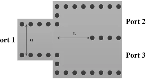
1.2 SIW power divider
The geometry of the SIW H-plane power divider is shown in Figure 1.2. A straight Y-junction [26] is adopted in the proposed power divider. The Y-junction consists of a bifurcated waveguide fed by a symmetrical step junction. Assuming that the dimension of SIW is chosen to support the TE10 mode exclusively in the selected frequency range, the total reflection of the TE20 mode will
occur, because there will be no TE10 mode on either side of the symmetrical step junction excited
L a
Port 2
Port 3
Port 1
Figure 1.2 Geometry of the SIW power divider
The width of the input and output SIW can be calculated according to the dielectric permittivity of the substrate and the center frequency of the power divider:
√ (1.2)
Where is the cutoff frequency of the SIW structure, is the relative dielectric constant of the substrate.
Distance L between the two discontinuities can be optimized to achieve the following goals: Minimize the reflection coefficient S11 at port 1
Keep the magnitudes of transmission coefficients S21 and S31 equal and close to -3
dB
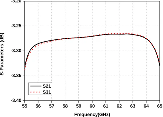
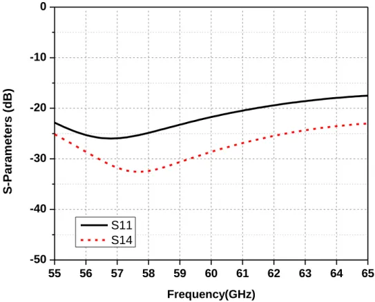
To evaluate the performance of the proposed power divider, S parameter simulation is executed by means of software HFSS. The center frequency is chosen at 60 GHz. Parameters of the power divider are listed in Table 1.1. The simulated S parameter results are shown in Figure 1.3 Figure 1.5.
Figure 1.3 shows that the magnitude of S11 is better than 20 dB over the 55-65 GHz frequency
range. Figure 1.4 shows that the transmission coefficients at different output ports are both around 3.3 dB, proving that the power split ratio is 1:1. Figure 1.5 shows that the signals at these two ports are in phase (the two curves are superposed).
Table 1.1 Dimension of the SIW power divider
Parameter Value 2.94 b 0.508 mm d 0.254 mm h 0.254 mm aeqv 2.6 mm a 2.73 mm L 3.7 mm
55 56 57 58 59 60 61 62 63 64 65 -50 -40 -30 -20 -10 0 S-Pa ra m e te rs (d B ) Frequency (GHz) S11
Figure 1.3 Simulated magnitude of S11 of the SIW power divider
55 56 57 58 59 60 61 62 63 64 65 -3.40 -3.35 -3.30 -3.25 -3.20 S-Par a m e te rs (d B ) Frequency(GHz) S21 S31
55 56 57 58 59 60 61 62 63 64 65 -200 -150 -100 -50 0 50 100 150 200 Ph a s e (D e g re e ) Frequency(GHz) S21 S31
Figure 1.5 Simulated phases of transmission coefficients of the power divider
The electric field distribution is shown in Figure 1.6. It can be seen that the magnitudes of electric field at two output ports are the same. Furthermore, they are in phase.
1.3 SIW hybrid coupler
The geometry of the targeted SIW hybrid coupler is shown in Figure 1.7. It is composed of two SIWs with a common wall on which an aperture is utilized to realize the coupling between the two SIWs at the output ports. The metallic vias close to the aperture are moved towards the aperture to control the coupling coefficient.
Ls
a
Port 1
Ws
Port 2
Port 3
Port 4
The width of the SIW hybrid coupler is the same as that of the SIW power divider. Step width
Ws and aperture length Ls are optimized to achieve the following coupling, reflection and
isolation requirements:
Minimize the reflection coefficient S11 at the port 1 and the isolation coefficient S41
between the port 1and the port 4
Keep the magnitudes of the transmission coefficients S21 and S31 equal and close to -3
dB
Keep the difference between the phases of S21 and S31 90°over the frequency range
S-parameters simulation of the designed coupler is made in HFSS at the center frequency 60 GHz. Parameters of the hybrid coupler are listed in Table 2.2. The simulated S parameter results are shown in Figure 1.8 Figure 1.10.
Table 1.2 Dimensions of the SIW hybrid coupler
Parameter Value 2.94 b 0.508 mm d 0.254 mm h 0.254 mm aeqv 2.6 mm a 2.73 mm Ls 2.7 mm Ws 0.78 mm
Figure 1.8 shows that the magnitude of S11 is better than 20 dB at 60 GHz and better than 17
dB over the frequency range, while the isolation between port 1 and port 4 is also better than 20 dB over the frequency range. Figure 1.9 shows that the transmission coefficients at port 2 and port 3 are both 3.3 dB, validating that the coupling ratio is 1:1. The difference between the phases of these two ports is close to 90 (89.7 at 60.5GHz), which agrees with the theoretical value very well. 55 56 57 58 59 60 61 62 63 64 65 -50 -40 -30 -20 -10 0 S-Pa ra m e te rs (d B ) Frequency(GHz) S11 S14 Figure 1.8 Simulated magnitudes of S11 and isolation between port 1 and port 4
55 56 57 58 59 60 61 62 63 64 65 -10 -8 -6 -4 -2 0 S-Pa ra m e te rs (d B ) Frequency(GHz) S21 S31
Figure 1.9 Simulated magnitudes of transmission coefficients of the hybrid coupler
55 56 57 58 59 60 61 62 63 64 65 -200 -150 -100 -50 0 50 100 150 200 Ph a s e (D e g re e ) Frequency(GHz) S21 S31
Figure 1.10 Simulated phases of transmission coefficients of the hybrid couple ≈90°
The electric field distribution is shown in Figure 1.11. It can be seen that the magnitudes of electric field at port 2 and port 3 are the same. Furthermore, there is a time delay in the output of port 3.
Figure 1.11 Electric field distribution of the hybrid coupler
1.4 SIW to microstrip line transition
Transitions from SIW to microstrip line are used to make the impedance matching at each port of the six-port circuit [27]. The tapered microstrip line transforms the TE mode in the SIW section to the quasi-TEM mode of the microstrip line. The geometry of a back-to-back SIW to microstrip line transition is shown in Figure 1.12.
Lm
W Wm
Port 1
Port 2
Length Lm and width Wm of the tapered part can be optimized to achieve the following goals: Minimize the reflection coefficient S11 at the port 1
Minimize the insertion loss S21 of the transition
To evaluate the performance of the transition, a back-to-back structure is designed and its S-parameters simulation is made in HFSS at the center frequency 60 GHz. The S-parameters of the power divider are listed in Table 1.3. The simulated S parameter results are shown in Figure 1.13 Figure 1.14.
Table 1.3 Dimensions of the transition
Parameter Value 2.94 b 0.508 mm d 0.254 mm h 0.254 mm W 0.66 mm Wm 1.02 mm Lm 0.98 mm
Figure 1.13 shows that the magnitude of S11 is better than 35 dB over the 55-65 GHz frequency
range. Figure 1.14 shows that the insertion loss between the input port and the output port of the transition is better than 0.3 dB over the frequency range. These results suggest that the transition has little influence on the whole six-port circuit.
55 56 57 58 59 60 61 62 63 64 65 -60 -50 -40 -30 -20 -10 0 S-Pa ra m e te rs (d B ) Frequency (GHz) S11
Figure 1.13 Simulated magnitude of S11of the transition
55 56 57 58 59 60 61 62 63 64 65 -0.30 -0.28 -0.26 -0.24 -0.22 -0.20 S-Pa ra m e te rs (d B ) Frequency(GHz) S21 Figure 1.14 Simulated insertion loss of the SIW power divider
The electric field distribution is shown in Figure 1.15. It can be seen that the electromagnetic field goes through the transition smoothly without a large reflection loss or a large insertion loss.
CHAPTER 2
MILLIMETER-WAVE SUBSTRATE INTEGRATED
WAVEGUIDE SIX-PORT CIRCUIT DESIGN
2.1 Introduction
The six-port circuits have been studied and developed since the 1970s [28]-[32]. It was first used by Cohn and Weinhouse to measure the phase of a microwave signal, and then developed by Engen and Hoer to obtain the complex reflection coefficients of a signal in microwave analysis. The six-port technologies were further developed by Professor R. G. Bosisio and collaborators, used as a microwave and millimeter-wave demodulator [33]. The six-port is a passive circuit, composed of hybrid couplers and/or power dividers with or without phase shifters. It has two inputs, one for the unknown signal and the other for the reference signal, and four outputs of linear combinations of two input signals.
Until now, six-port circuits have been developed in many applications. It can be utilized as both standard frequency modulation continuous wave (FMCW) radar sensor and direct down-conversion receiver. In addition, the six-port receiver can demodulate signals in different formats, including binary phase shift keying (BPSK), quadrature phase shift keying (QPSK), and quadrature amplitude modulation (QAM). Previous studies show that six-port circuits can be implemented with different fabrication technologies. For example, miniaturized hybrid microwave integrated circuit (MHMIC) and monolithic microwave integrated circuit (MMIC) technology were used for QPSK demodulation in Ka-band six-port front end modules [34], machined WR-10 waveguides were used for the design of a collision avoidance continuous wave (CW) radar sensor in W-band [35], SIW structure was also used for QPSK, QAM16 and orthogonal frequency division multiplexing (OFDM) demodulation in Ka-band software defined radio (SDR) receivers [36]-[37], and so on.
Millimeter-wave six-port circuit is an innovative approach in wireless communication. Many previous research results demonstrated that the six-port down-converter can work well when the local oscillator (LO) power is as low as -25 dBm, compared to conventional techniques with anti-parallel diodes (the LO power is at least +10 dBm for achieving the same conversion loss). The excellent isolation between the unknown signal and the reference signal (up to 40 dB in certain implementations) is another important advantage.
The entire six-port circuit is presented in this chapter. It is designed based on the previous analysis and design of the millimeter-wave SIW power divider and hybrid coupler. By using commercial software HFSS 15.0, the six-port circuit is designed and optimized over the 60-63 GHz frequency range.
2.2 Six-port circuit theory
In the previous studies, six-port circuits have been demonstrated as an excellent candidate for microwave and millimeter-wave modulator and demodulator for both communication and radar systems.
When the six-port circuits work as modulators, the outputs of the hybrid couples are connected to two pairs of mono-ports, having adjustable reflection coefficients. Different modulation signals (such as QPSK, 8PSK, and 16QAM) can be obtained by using different reflection coefficients that are only real part values. For example, the QPSK signal is produced if the pair of reflection coefficients is 1 and -1 (open and short circuits, respectively).
When they work as demodulators, there are three types of block diagrams to design and apply six-port circuits according to the design situation as follows:
Three couplers power divider
Two couplers two power dividers 90° phase shifter Four couplers 90° phase shifter
The three types of six-port circuit have been widely applied at microwave and millimeter- wave frequency. Each of them has its own features, including advantages and disadvantages:
For the first type, no phase shifter is required.
For the second type, no additional matching load is required. For the third type, no power divider is required.
1 2 3 4 5 6 7 8 9 10 (a) Type 1 90° Power Divider Hybrid Coupler Phase Shifter 1 2 3 4 5 6 7 8 9 10 (b) Type 2
90° 1 2 3 4 5 6 7 8 9 10 (c) Type 3
Figure 2.1 Block diagram of three types of six-port circuit
The analysis of the six-port circuit is shown by calculating the S parameter matrix of the first type. The other two types of six-port junctions can be analyzed through the same process.
The S parameter matrix of the power divider is given in 2.1:
√
[
]
(2.1)
√
[
] (2.2)
To obtain the S parameter matrix of the entire six-port junction, all the input ports, the intermediate ports and the output ports are numbered, as shown in Figure 2.1. The incident wave and reflected wave at each port are defined as and , .
From 2.1 and 2.2, the incident waves at port 7 to port 10 can be expressed as:
√
√
√
(2.3)
√
Then the reflected waves at port 1 to port 6 can be expressed as:
(
) (2.4)
(
)
(
)
Since
[ ] [ ][ ] (2.5)
The S parameter matrix of the first type can be listed as follows:
[
]
[
]
[
]
(2.6)
The S parameters of the other types of six-port junction can be calculated in the same way as the first one:
For model 2, the incident waves at the intermediate ports can be expressed as:
√
√
(2.7)
√
The reflected waves at the output ports are expressed as:
(
)
(
) (2.8)
(
)
(
)
The S parameter matrix of the second type can be listed as follows:
[
]
[
]
[
]
(2.9)
For model 3, the incident waves at the intermediate ports can be expressed as:
√
√
√
(2.10)
√
The reflected waves at the output ports are expressed as:
(
)
(
) (2.11)
(
)
(
)
The S parameter matrix of the third type can be listed as follows:
[
]
[
]
[
]
(2.12)
The phases from two input ports to four output ports are critical in order to determine the demodulation results of the six-port junction. The phases can be obtained from the S parameter matrix. For example, for the first type, the phase differences between adjacent output ports are shown as follows:
(
) (
)
(
) (
) (2.13)
(
) (
)
(
) (
)
The three previous S parameter matrices are generated for the ideal cases that all the input ports and output ports are connected to perfect matching loads. However, in the application of a six-port receiver, four output ports are connected to other circuits such as power detectors, which sometimes have a limited matching condition. In these cases, a matching network is necessary to reduce undesired reflections.
2.3 SIW six-port circuit
The topology of the proposed SIW six-port circuit is shown in Figure 2.2. It consists of two SIW power dividers [38], two SIW hybrid couplers and the phase shifters. The ° phase shifters are realized by the additional SIW transmission lines. There are four circular corners after the power dividers to lead the signal to the hybrid couplers. SIW to microstrip line transitions are applied at each port of the six-port circuit for measurement purpose. The output ports of the hybrid coupler are bent and separated enough to support the use of V connectors (with a 0.375 inch square flange). The layout of the whole SIW six-port circuit is shown in Figure 2.3. Port 1 45° -45° Port 2 Port 3 Port 4 Port 5 Port 6 Power Divider Hybrid Coupler Phase Shifter
Port 1
Port 2
Port 3
Port 5
Port 4
Port 6
Figure 2.3 Layout of the proposed six-port circuit
-45°
The selection of the parameters that are optimized to improve the performance of the six-port circuit is based on the previous design of power divider and hybrid coupler. However, after integrating all the parts, some of the parameters (such as the step width Ws and the aperture length La of the hybrid coupler) have to be tuned again according to the following design requirement:
Minimize the reflection coefficient S11 at port 1 and S22 at port 2, and the isolation
coefficient S21 between the port 1 and port 2
Keep the magnitudes of transmission coefficients S31 to S61 and S32 to S62 equal and
close to -6 dB
Keep the difference of phases between the input ports (port 1 and port 2) and the output ports (port 3, 4, 5, 6) the same as the theoretical values (see Table 2.1)
Table 2.1 Theoretical phase values of the six-port circuit S parameter Phase (degree)
S31 180 S41 90 S51 90 S61 180 S32 0 S42 90 S52 180 S62 90
The S-parameters simulation of the six-port is made in HFSS at center frequency 61 GHz. The final dimension of the six-port circuit is listed in Table 2.2. The simulated S parameter results are shown in Figure 2.4 Figure 2.8.
Table 2.2 Dimension of the six-port circuit Parameter Value 2.94 b 0.508 mm d 0.254 mm h 0.254 mm aeqv 2.6 mm a 2.73 mm L 3.8 mm Ls 2.92 mm Ws 0.48 mm W 0.66 mm Wm 1.15 mm Lm 1.3 mm
Figure 2.4 shows magnitudes of S11、S22 and the isolation between the two input ports (port1
to port 2) over the 60-63 GHz frequency range. It can be found that the magnitudes of S11 and S22
are better than 25 dB at the selected 60.5 GHz and better than 20 dB over the frequency range, while the isolation between these ports is 27 dB at 60.5 GHz and better than 20 dB over the frequency range.
Figure 2.5 and Figure 2.6 show the magnitudes of transmission coefficients S31 to S61 and S32
to S62 over the 60-63 GHz frequency range. It can be found that the transmission coefficients are
around 6 dB at 60.5 GHz, which is very close to the theoretical values. They are located around -6 dB within an acceptable frequency range.
Figure 2.7 and Figure 2.8 show the phases of transmission coefficients S31 to S61 and S32 to S62
over the 60-63 GHz frequency range. It can be found that the phases of the transmission coefficients match the theoretical values at 60.5 GHz, which means that the phase shifters are designed appropriately. They have a maximum error of 15°over the frequency range.
60 61 62 63 -40 -35 -30 -25 -20 -15 -10 -5 0 S-Pa ra m e te rs (d B ) Frequency(GHz) S11 S12 S22
Figure 2.4 Simulated magnitudes of S11 、S22 and the isolation between the two input ports
60 61 62 63 -12 -11 -10 -9 -8 -7 -6 -5 -4 -3 -2 -1 0 S-Par a m te rs (d B ) Frequency(GHz) S31 S41 S51 S61 Figure 2.5 Simulated magnitudes of transmission coefficients S31 to S61
60 61 62 63 -12 -11 -10 -9 -8 -7 -6 -5 -4 -3 -2 -1 0 S-Par a m e te rs (d B ) Frequency(GHz) S32 S42 S52 S62
Figure 2.6 Simulated magnitudes of transmission coefficients S32 to S62
60 61 62 63 -200 -150 -100 -50 0 50 100 150 200 Ph a s e (D e g re e ) Frequency(GHz) S31 S41 S51 S61
60 61 62 63 -200 -150 -100 -50 0 50 100 150 200 Ph a s e (D e g re e ) Frequency(GHz) S32 S42 S52 S62
Figure 2.8 Simulated phases of transmission coefficients S32 to S62
2.4 Measurement results of the SIW six-port circuit
The SIW six-port circuit was fabricated on a Rogers RT/duroid 6002 Laminates substrate with dielectric permittivity of 2.94 and substrate thickness of 10 mils. The total size of the six-port circuit with the transitions is 43mm 53mm 0.254mm.The fabrication was done by employing a laser micromachining technique which executed a complex shaped perforation. The prototype of the fabricated SIW six-port circuit and the TRL (through-reflection-line) calibration circuit are shown in Figure 2.9.
Our Anritsu 37397C network analyzer is used for S parameter measurements. V (1.85 mm) connectors (from “Southeast Microwave”) are placed at each port of the six-port circuit for measurement purpose. The TRL calibration method is used to get rid of the influence of the SIW to microstrip line transitions by setting the reference plane after the transitions. The measurement setup of the SIW six-port circuit is shown in Figure 2.10. Measurement results are shown in Figure 2.11 Figure 2.15.
(a)
(b)
Figure 2.10 Measurement setup of the fabricated six-port circuit
Figure 2.11 shows the magnitudes of S11、S22 and the isolation between the two input ports
(port 1、port 2) over the 60-63 GHz frequency range. It can be found that the magnitudes of S11
and S22 are better than 10 dB over the frequency range, while the isolation between these ports is
also better than 10 dB over the frequency range. The simulated and measured results match each other very well.
Figure 2.12 and Figure 2.13 show the magnitudes of transmission coefficients S31 to S61 and
S32 to S62 over the 60-63 GHz frequency range. The transmission coefficients are around -6 dB at
60.5 GHz and within an acceptable frequency range. The simulation and measurement results agree well.
60 61 62 63 -45 -40 -35 -30 -25 -20 -15 -10 -5 0 S-Pa ra m e te rs (d B ) Frequency(GHz) S11 S12 S22
Figure 2.11 Measured magnitudes of S11、S22 and the isolation between the two input ports
60 61 62 63 -16 -14 -12 -10 -8 -6 -4 -2 0 S-Par a m e te rs (d B ) Frequency(GHz) S31 S41 S51 S61
60 61 62 63 -16 -14 -12 -10 -8 -6 -4 -2 0 S-Par a m e te rs (d B ) Frequency(GHz) S32 S42 S52 S62
Figure 2.13 Measured magnitudes of transmission coefficients S32 to S62
Figure 2.14 and Figure 2.15 show the phases of transmission coefficients S31 to S61 and S32 to
S62 over the 60-63 GHz frequency range. It can be found that the phases of the transmission
coefficients match the theoretical values at 60.5 GHz. The phase differences between S31 and S41,
S51 and S61, S32 and S62 are close to zero, while the phase differences between S31 and S51, S41 and
60 61 62 63 -200 -150 -100 -50 0 50 100 150 200 Ph a s e (D e g re e ) Frequency(GHz) S31 S41 S51 S61
Figure 2.14 Measured phases of transmission coefficients S31 to S61
60 61 62 63 -200 -150 -100 -50 0 50 100 150 200 Ph a s e (D e g re e ) Frequency(GHz) S32 S42 S52 S62
We find out from the measurement results that the six-port circuit works well over 60-63 GHz frequency range. The next discussion will demonstrate that the fabricated six-port can support future MIMO system analysis. However, some of the curves show unexpected behaviors. The possible reasons are given as follows:
The used V connectors are not identical. When the V connectors are connected to the six-port circuit, there is always additional effect resulting from the discontinuity between them.
The four 50 loads that are connected to unmeasured ports are not good and identical. There are two male loads and two female loads, which means that additional errors could be brought to the measured phases due to the use of two transitions. Once the impedance of the loads was no longer 50 , the reflection of the signals could happen at the end of the loads, resulting in deterioration of the performance of the six-port circuit. Figure 2.16 shows the changes of simulation isolation between input ports and transmission coefficients between input ports and output ports. In this case, the impedance of the loads that are connected to port 4 and port 6 is 15 .
Additional losses of the circuit during the measurement process are relatively high at 60 GHz, which makes the TRL calibration difficult to realize.
60 61 62 63 -40 -35 -30 -25 -20 -15 -10 -5 0 S-Pa ra m e te rs (d B ) Frequency(GHz) S11 S12 S22 (a)
60 61 62 63 -16 -14 -12 -10 -8 -6 -4 -2 0 S-Par a m e te rs (d B ) Frequency(GHz) S32 S42 S52 S62 (b) 60 61 62 63 -200 -150 -100 -50 0 50 100 150 200 Ph a s e (D e g re e ) Frequency(GHz) S32 S42 S52 S62 (c)
Figure 2.16 Simulation results of the six-port circuit with imperfect loads (a) magnitudes of S11, S22 and S12; (b) magnitudes of S32 to S62; (c) phases of S32 to S62
2.5 Performance study of the six-port circuit for future MIMO systems
As known, the design criterion of a six-port consists of achieving a specific distribution of the points. In general, a very good performance is obtained when the points are equidistant from the origin and angularly spaced by 360º divided their number (i = 4 in this case) [39]. When the RF and the LO ports are isolated, the points of the six-port can be expressed in terms of S parameters in the following:
(2.13)
The calculation of points corresponding to this design shows that they are located on the unitary circle at [( ) ] . For comparison, the plots of the points based on measurements from 60 GHz to 60.5 GHz are shown in Figure 2.17. As seen, the magnitudes of the points are located around 1 (with maximum deviation 105.6%), while the argument difference is close to 90º between two corresponding points (with maximum deviation 47.6 ). The errors are produced by the measured phases of transmission coefficients S32 to S62. In spite of
this, the points are located in different quadrant, which suggests that the six-port circuit can be applied in the millimeter-wave MIMO systems.
Figure 2.17 Polar plots of the measured points of the proposed six-port
-2 -1 0 1 2 -3 3 freq (60.00GHz to 60.50GHz) m a g g m a g g 1 m a g g 2 m a g g 3 (0.000 to 0.000) m a g g 4 m a g g 5 m a g g 6 m a g g 7 qi p o in ts ( i=3 t o 6) Re Im X Ideal qi Measured qi
The six-port output voltages versus the phase differences between two RF input signals are presented in Figure 2.18. The RF source is equally split into two signals, with one of them controlled by a phase shifter. One of them is connected to the RF signal input port of the six-port circuit, while the other of them is connected to the reference signal input port.
Output voltages are shown in Figure 2.19. The output voltage minimum value points are close to 0 and shifted by ° multiples. In addition, the phases of output voltages at the pairs of ports 3 and 5, 4 and 6 are opposite to each other, respectively. Therefore, I/Q output signals can be obtained by this structure.
six-port
circuit
power
divider
phase
shifter(F )
P1
P2
V3
V4
V5
V6
0 30 60 90 120 150 180 210 240 270 300 330 360 0.000 0.025 0.050 0.075 0.100 Vo u t(V) F(deg)
Figure 2.19 Six-port output voltages versus phase differences
The performance study of the fabricated six-port circuit has shown that it is operating well at 60.5 GHz. The distribution of points and output voltage minimum positions suggest that the six-port circuit can offer good quadrature outputs that are applied in the MIMO system.
V3
CHAPTER 3
SIX-PORT TECHNOLOGY FOR MILLIMETER-WAVE
MIMO SYSTEMS
3.1 Introduction
In modern wireless communication system, the requirements for data rata are getting higher and higher. For example, more and more people are requiring huge data file transmission and real-time video streaming to support their work and entertainment that are becoming faster and faster. Recently, tens of Mbps (mega bit per second) date rate can be realized easily, while hundreds of Mbps capacities are possible with the fast developing IEEE 802.11n Wireless Local Area Network technology. However, these data rates are much lower than the 10-160 Gbps (giga bit per second) scenarios that are provided by optical links.
At the same time, millimeter-wave wireless communication is attractive for its high speed data rate to bridge the gap of channel capacity between lower frequencies and optical links. There have been published studies that realize the speed of the order of Gbps [40], [41]. For example, a 1.25 Gbps 60 GHz-band full duplex wireless Gigabit Ethernet link has been reported in [42], in which direct ASK modulation and demodulation are adopted for the transceiver. A 60 GHz MMIC chipset for radio and radar application is presented in [43], in which the data rate can reach 1 Gbps using Agilent’s advanced e-beam pseudomorphic high electron mobility transistor (PHEMT) process. A 2 Gbps 60 GHz low power ultra-broadband transceiver is reported in [44], and the transceiver including antennas is fabricated in complementary metal-oxide-semiconductor (CMOS) [45]-[48] 65 nm SOI (silicon on insulator) and packaged in quad flat no-lead (QFN). Furthermore, the transceiver power efficiency is lower than 50 pJ/bit as a result of scalable power consumption that is realized by pulse generator and super regenerator oscillator architecture. A 4 Gbps 60 GHz transmission is presented in [49], in which the transmission supports the uncompressed video signal over an orbital angular momentum (OAM) wireless channel; the potential ability of spatial multiplexing based on OAM and holographic beam-forming will be a candidate for future communication. A 2 Gbps 60 GHz transmission is reported in [50], in which the channel supports the uncompressed HDTV signal by using a 60 GHz SiGe radio chipset; the baseband was equipped with both efficient random packet error recovery and symbol-timing recovery, in order to prevent more errors in high speed data rate.
Although a high data rate transmission can be easily realized in single millimeter-wave link application, we cannot rely on it any more if the data rate keeps increasing, while the simple installation is maintained. Then, the millimeter-wave MIMO system is presented to satisfy the requirement of an extremely high data rate. On one side, conventional MIMO operating at RF and low-end microwave frequencies [51], [52] is a mature technology that makes use of multiple antennas to exploit multipath effects. On the other side, the emerging millimeter-wave MIMO is a candidate of choices to support multi-Gb/s data rate in both indoor and outdoor environments. Our purpose in this chapter is to highlight how millimeter-wave MIMO system differs from that working at lower frequencies.
The analysis of the difference between millimeter-wave MIMO systems and MIMO systems at lower frequencies can start with the Friis formula:
(
)
(3.1)
Where is the total power from the transmitter, is the received power on the receiver with its terminal impedance, denotes the transmitter antenna directivity, denotes the receiver antenna directivity, is the wavelength at the working frequency, and is the distance between the transmitter and the receiver.
In practice, the transmitter and receiver antenna directivities are stated in decibels, as are the transmitted and received powers. Then the Friis formula can be expressed in decibels as follows:
(
)
Compared to the systems operating at lower frequencies such as 5 GHz, those operating at 60 GHz have a propagation loss of 21.58 dB or higher, for the same transmitter and receiver antenna directivity. Furthermore, compared to conventional MIMO, the millimeter-wave MIMO [53]-[54] have channels that are characterized by LoS (line-of-sight) or near LoS. Hence, spatial multiplexing can no longer be obtained through a rich scattering environment. Instead, it can be obtained by focusing the receiver antenna array on a different transmitter antenna array [55]-[57]. This is beneficial to systems which cannot make use of a spatial multiplexing deriving from the independent and identically distributed flat Rayleigh fading channels.
Millimeter-wave MIMO system has been studied in previous work. The channel modeling was studied for millimeter-wave MIMO in [58], in which two kinds of scenario were examined to observe the consequences of the MIMO LoS channels, or more generally, sparse scattering channels that have antennas with moderate separation in both indoor and outdoor environment. The results are different from the existing lower frequency MIMO systems because some special paths are dominant for the directional millimeter-wave MIMO transmission, compared to a rich scattering environment at lower frequencies. The crosstalk of the millimeter-wave MIMO system was discussed in [59], and the results demonstrated that linear MIMO crosstalk was relatively benign, as a result of being corrected by the MIMO equalizers, while nonlinear crosstalk would be much more harmful to the system that was not corrected by the MIMO equalizers. In addition, it is not feasible to realize a high precision analog/digital (AD) conversion of millimeter-wave signals by using the current technologies. Therefore, it is necessary to perform most of the signal processing to separate the data signals from different transmitters in the analog section instead of in the digital section.
The proposed system uses two six-port quadrature receivers to increase the MIMO system diversity, as explained in detail in this chapter. As it is known, the six-port is a passive circuit that acts as an interferometer; its output signals are linear combinations of phase shifted reference and input unknown signals. By using appropriate devices connected to output ports, this circuit can provide quadrature down conversion or direct modulation. The wide bandwidth, the reduced local oscillator power requirement and the very good isolation between RF inputs can be derived from its intrinsic properties.