Université du Québec
Institut National de la Recherche Scientifique Centre Énergie Matériaux Télécommunications
A Broadband Direct-Demodulator Based on Nolen Matrix for 5G Wireless
Communication Systems
Par
Esam Abdusalam Shafah
Mémoire présentée pour l’obtention du grade de Maître ès sciences (M.Sc.)
En Télécommunications
Jury d’évaluation
Président du jury et examinateur interne
Professeur Tayeb A. Denidni INRS-EMT
Examinateur externe Professeur Halim Boutayeb
Huawei Technologies Canada Co., Ltd.
Directeur de recherche Professeur Tarek Djerafi INRS-EMT
III
Abstract
The development of low cost, low power receiver (low power signal demodulation) is indispensable for the next generation of wireless communication, which is defined as a green communication system. The multiport reflectometer is a measurement device that mainly used in high-frequency bands. This technique allows the measurement of the amplitude ratio and the phase difference of two electromagnetic waves. Besides, it can be used as a direct demodulator. The framework of the conventional six-port is not adapted to millimeter-wave applications. In fact, the input and output ports arrangement are not suitable for the integrated system where both inputs and output are not separated.
A new multi-port reflectometer based on Nolen matrix with a centre frequency of 28 GHz is proposed and analyzed. The Input and output ports are rearranged separately. The two inputs represent the local oscillator (LO) and the radio frequency (RF) signals, where RF and LO signals are fed to the inputs (port 6 and port 1), respectively. In addition, I and Q signals are retrieved after the detection stage at the four output ports (ports 2 - 5). The obtained structure represents the aimed arrangement in terms of suitability of use when inputs and outputs are separated each in one side, and good performance is fulfilled.
The designed 2x4 Nolen matrix consists of five hybrid couplers (two 3dB, two 4.7 dB, and one 6 dB) and the proposed double T-shape phase shifter. The circuit is simulated and fabricated to validate the introduced scheme. Advanced Design System (ADS) software is used to design the different components. Both processes, the simulation and the fabrication, have shown a good agreement in terms of retrieving the original signal and implying the aimed arrangement. The obtained results of isolation are better than 20 dB for the frequency range from 26 GHz to 30.4 GHz. Good power equality is achieved of less than 1.5 dB around 7.5 dB of supplemental insertion loss and phase unbalance of ± 8 degree.
The proposed circuit is low cost, small size simple structure with good performance and suitable configuration arrangement with separate inputs and outputs. This study has been made to show that the proposed multi-port based on Nolen matrix can be more adequate for the next generation millimeter wave communications compared to the conventional millimeter wave receivers.
Keywords: Advanced Design System (ADS), Multi-port receiver, local oscillator (LO), radio
V
DEDICATION
Praise be to Allah and prayer and peace be upon the Messenger of Allah. Then, I
dedicate this work to my mother, may Allah prolong her life in his obedience and my father
may Allah have mercy on him. Since this is a little of what I have been given. I also pay
tribute to my wife who sacrificed and still sacrificing for me. I thank my dear sons and
daughters for their inspiration. Thanks to my siblings for their continued support.
VI
ACKNOWLEDGEMENT
In the name of Allah, I thank Allah for his mercy, which made my able to go through
this challenge up to the end.
I would like to express my gratitude to my research supervisor Prof. Tarek Djerafi for
his unlimited support, guidance, and continuous advice during my research activities. In
addition, I would like to thank the jury members for their time and efforts in reviewing my
thesis and providing me valuable comments. Thanks to all my colleagues at INRS-EMT
whom have helped me directly or indirectly in the completion of my thesis. In additional
to all INRS staff.
VII
TABLE OF CONTENTS
1
CHAPTER ONE: INTRODUCTION ... 1
5G Technology ... 1
5G spectrum availability ... 3
1.2.1 28 GHz frequency band (27.5-28.35 GHz) ... 3
1.2.2 Frequency band 37-40 GHz ... 4
1.2.3 Frequency band 64-71 GHz for license-exempt use ... 6
Architectures of reception systems ... 7
1.3.1 Homodyne receivers (direct conversion or ZERO-IF) ... 8
1.3.2 Heterodyne receivers ... 9
1.3.3 Direct receiver (Demodulator) ...10
Millimeter wave demodulator ... 13
Proposed work ... 15
2
CHAPTER TWO: Design of Nolen Matrix ... 17
Multi-port beamforming ... 17
BFN matrices ... 17
2.2.1 Butler matrix ...17
2.2.2 Blass matrix ...19
2.2.3 Nolen Matrix ...20
Nolen matrix as demodulator ... 20
2.3.1 Six port demodulator ...21
Design of Nolen matrix (using ideal components) ... 24
Six port based on Nolen matrix with ideal components ... 26
3
CHAPTER THREE: Building Multi-Port System ... 29
Directional coupler ... 29
VIII
3.2.1 Hybrid coupler (3dB, 90 °) ...30
3.2.2 Hybrid coupler (4.7dB, 90 °) ...32
3.2.3 Hybrid coupler (6 dB, 90 °) ...33
Phase shifter ... 34
3.3.1 Schiffman phase shifter ...34
3.3.2 Modified Schiffman phase shifter ...36
3.3.3 Double T - shape phase shifter ...37
3.3.4 Double T-shape phase shifter 90 0 ...37
Designed Nolen matrix using ADS ... 39
4
CHAPTER FOUR: Experimental Validation ... 43
Fabricated circuit ... 43
Experimental results ... 44
Constellation ... 48
5
CHAPTER FIVE: Contributions and Future Work ... 51
Contributions ... 51
Future work... 52
6
CHAPTER SIX : Résumé ... 53
INTRODUCTION ... 53
6.1.1 Technologie 5G ...53
6.1.2 Disponibilité du spectre 5G ...54
6.1.3 Sélection de fréquence ...56
6.1.4 Architectures des systèmes de réception ...56
6.1.5 Démodulateurs à ondes millimétriques ...58
CHAPITRE DEUX : Conception de la matrice de Nolen ... 59
6.2.1 Formation de faisceaux ...59
Matrice de Butler ...59
IX
Matrice de Nolen ...60
6.2.2 Matrice de Nolen comme démodulateur...61
6.2.3 Démodulateur à six ports ...62
6.2.4 Conception de la matrice Nolen (utilisant des composants idéaux) ...63
6.2.5 Six ports basés sur la matrice Nolen avec des composants idéaux ...65
CHAPITRE TROIS : Design de la matrice de Nolen ... 67
6.3.1 Coupleur directionnel ...67
6.3.2 Coupleur à interaction localisée à 7 lignes de transmission (deux sections) .67 6.3.3 Déphaseur ...69
6.3.4 Matrice Nolen conçue à l’aide de l’ADS ...71
Validation expérimentale ... 73
6.4.1 Circuit fabriqué...73
6.4.2 Résultats ...74
6.4.3 Constellation ...78
6.4.4 Contributions et travaux futurs ...79
X
LIST OF TABLES
TABLE 1.1 TABLE OF THE CURRENT AND NEXT TECHNOLOGY (5G) ... 1 TABLE 1.2 PERFORMANCE COMPARISON OF HETERODYNE, HOMODYNE AND MULTIPORT
TECHNIQUES (WITH REFERENCE TO DIODE-BASED RECEIVER ARCHITECTURES) ...14 TABLE 2.1 PARAMETERS OF THE NOLEN 2X4MATRIX RETAINED (ΘIJ ANDɸIJ)[23] ...24
XI
TABLE OF FIGURES
FIGURE 1.1 5G SERVICE TRENDS [7]. ... 2
FIGURE 1.2 CANADIAN FREQUENCY ALLOCATIONS IN THE 28GHZ BAND [5]. ... 4
FIGURE 1.3 CURRENT CANADIAN BAND PLAN IN THE FREQUENCY BAND 27.5-28.35GHZ [5]. ... 4
FIGURE 1.4 PROPOSED NEW CANADIAN BAND PLAN IN THE 28GHZ BAND [5]. ... 4
FIGURE 1.5 CURRENT USE OF THE FREQUENCY BAND 37-40GHZ BY FIXED SERVICE [5]. ... 5
FIGURE 1.6 PROPOSED CANADIAN 37-40GHZ FREQUENCY BAND PLAN [5]. ... 5
FIGURE 1.7 CANADIAN FREQUENCY ALLOCATIONS IN THE BAND 64–71GHZ [5]. ... 6
FIGURE 1.8 RADIO ACCESS VISION FOR 2020 AND PAST:5GRADIO ACCESS CONTAINS A NEW RADIO ACCESS TECHNOLOGY (NR) AND LTEEVOLUTION THAT IS NOT IN REVERSE GOOD WITH LTE AND IS OPERABLE FROM SUB-1GHZ TO 100GHZ [8]. ... 7
FIGURE 1.9 ARCHITECTURES OF RECEPTION SYSTEMS [10]. ... 7
FIGURE 1.10 ARCHITECTURES OF HOMODYNE RECEIVERS [10]. ... 8
FIGURE 1.11 ARCHITECTURES OF HETERODYNE RECEIVERS [10]. ... 9
FIGURE 2.1 A STANDARD TOPOLOGY OF NXNBUTLER MATRIX. ...18
FIGURE 2.2 TOPOLOGY OF BLESS MATRIX. ...19
FIGURE 2.3 THE GENERAL FORM OF THE NOLEN MATRIX.[16] ...20
FIGURE 2.4 A DIAGRAM SHOWING THE ADS SIMULATION OF THE MULTI-PORT DIRECT CONVERSION WITH IDEAL SIX-PORT. ...21
FIGURE 2.5 SUBTRACTION AND AMPLIFICATION CIRCUIT USING OPERATIONAL AMPLIFIERS. ...21
FIGURE 2.6 INPUT AND OUTPUT SIGNALS (A)IINPUT/IOUTPUT IN VOLT VS. TIME AND (B)QINPUT/QOUTPUT IN VOLT VS. TIME. ...22
FIGURE 2.7 SPECTRUM OF THE INPUT QPSK MODULATED SIGNAL. ...23
FIGURE 2.8 SPECTRUM OF THE QPSK DEMODULATED SIGNALS (IOUT AND QOUT) AT THE OUTPUT AND THE INPUT LO SIGNAL (VIN). ...23
FIGURE 2.9 BUILDING NOLEN MATRIX USING ON ADS(IDEAL CASE). ...24
FIGURE 2.10 SIMULATED RELATIVE PHASE DIFFERENCES BETWEEN (A) ADJACENT OUTPUT PORTS FOR PORT1, AND (B) ADJACENT OUTPUT PORTS FOR PORT 6. ...25
FIGURE 2.11 SIX PORT BASED ON NOLEN MATRIX USING IDEAL COMPONENTS. ...26
FIGURE 2.12 INPUT AND OUTPUT SIGNALS (A)IINPUT/IOUTPUT IN VOLT VS. TIME AND (B) QINPUT/QOUTPUT IN VOLT VS. TIME. ...27
XII
FIGURE 2.14 SPECTRUM OF THE OUTPUT QPSK DEMODULATED SIGNALS (IOUT AND QOUT) AND THE
INPUT SIGNAL (VIN). ...28
FIGURE 3.1 SINGLE SECTION 3 DBHYBRID COUPLERS 90°. ...29
FIGURE 3.2 LAYOUT OF DESIGNED HYBRID COUPLERS 90°. ...30
FIGURE 3.3 SIMULATION OF HYBRID COUPLER (3DB,90°) IN ADS. ...31
FIGURE 3.4 THE LAYOUT OF THE HYBRID COUPLER 3DB SHOWING DETAILS ABOUT DIMENSIONS IN (MM) AND IMPEDANCE IN (OHM). ...31
FIGURE 3.5 THE SIMULATED RESULTS SHOWING S PARAMETER OF COUPLER 3 DB. ...31
FIGURE 3.6 SIMULATION CIRCUIT OF HYBRID COUPLER (4.7DB,90°) IN ADS. ...32
FIGURE 3.7 THE LAYOUT OF THE HYBRID COUPLER 4.7 DB SHOWING DETAILS ABOUT DIMENSIONS IN (MM) AND IMPEDANCE IN (OHM). ...32
FIGURE 3.8 THE SIMULATED RESULTS SHOWING S PARAMETER OF COUPLER 4.7 DB. ...33
FIGURE 3.9 SIMULATION CIRCUIT OF HYBRID COUPLER (6 DB,90°) IN ADS ...33
FIGURE 3.10 THE LAYOUT OF 6 DB HYBRID COUPLER SHOWING DETAILS ABOUT DIMENSIONS IN (MM) AND IMPEDANCE IN (OHM). ...34
FIGURE 3.11 THE SIMULATED RESULTS SHOWING S PARAMETER OF COUPLER 6 DB. ...34
FIGURE 3.12 THE STANDARD STRUCTURE OF 900SCHIFFMAN PHASE SHIFTER. ...35
FIGURE 3.13 COUPLED-TRANSMISSION-LINE ELEMENT WITH ENDS CONNECTED AND CURVES OF ITS PHASE RESPONSE FOR THREE VALUES OF (Ρ =𝑍0𝑒𝑍0𝑜)[30]. ...36
FIGURE 3.14 SOME ALTERNATIVES TO OBTAIN A DIFFERENTIAL PHASE SHIFTER:(A)STANDARD SCHIFFMAN PHASE SHIFTER,(B)DOUBLE SCHIFFMAN PHASE SHIFTER,(C)SCHIFFMAN PHASE SHIFTER WITH CASCADED SECTIONS, AND (D)PARALLEL SCHIFFMAN PHASE SHIFTER [33]. ...36
FIGURE 3.15 A900SCHIFFMAN PHASE SHIFTER LAYOUT USING A PATTERNED GROUND PLANE [32]. ...37
FIGURE 3.16 THE LAYOUT OF THE PROPOSED 90° DOUBLE PARALLEL DOUBLE T-SHAPE PHASE SHIFTER WITH CONSIDERING THE SYMMETRY FOR EACH ELEMENT. ...38
FIGURE 3.17 SIMULATED RESULTS OF THE PROPOSED 90T-PHASE SHIFTER.(A)AMPLITUDE RESPONSE.(B)PHASE RESPONSE. ...39
FIGURE 3.18 THE LAYOUT OF THE SIX-PORT DEMODULATOR BASED ON NOLEN MATRIX. ...40
FIGURE 3.19 THE ELECTRIC FIELD DISTRIBUTION (A) WHEN PORT 1 EXCITED (B) WHEN PORT 6 EXCITED ...41
FIGURE 4.1 PHOTOGRAPH OF THE FABRICATED CIRCUIT. ...43
FIGURE 4.2 INPUT MATCHING): A)SIMULATED, B)MEASURED. ...44
XIII
FIGURE 4.4 TRANSMISSION COEFFICIENT (AMPLITUDE): A)SIMULATED PORT 1, B)MEASURED
PORT1, C)SIMULATED PORT 2, D)MEASURED PORT 2. ...45
FIGURE 4.5 TRANSMISSION COEFFICIENT (PHASE): A)SIMULATED PORT 1, B)MEASURED PORT2, C) SIMULATED PORT 2, D)MEASURED PORT 2...46
FIGURE 4.6 BLOCK DIAGRAM DISPLAYING THE MULTI-PORT OUTPUT VOLTAGES. ...47
FIGURE 4.7 NOLEN MATRIX AS PHASE DISCRIMINATOR. ...47
FIGURE 4.8SIMULATED CONSTELLATIONS OF THE DEMODULATED SIGNAL CONSIDERING IDEAL AND MEASURED S-PARAMETERS OF THE PROPOSED NOLEN MATRIX (BPSK,QPSK, AND 8PSK). .. 40
MHZ OF DATA RATE IS CONSIDERED WITH 150 M OF DISTANCE BETWEEN THE TRANSMITTER AND RECEIVER WITH FREE SPACE CHANNEL. ...49
FIGURE 6.1 TENDANCES DES SERVICES 5G[6]. ...54
FIGURE 6.2 VISION DE L'ACCES RADIO POUR 2020 ET LES ANNEES PRECEDENTES:L'ACCES RADIO 5G CONTIENT UNE NOUVELLE TECHNOLOGIE D'ACCES RADIO (NR) ET UNE EVOLUTION LTE QUI N'EST PAS INVERSEE ET QUI FONCTIONNE DE 1GHZ A 100GHZ [7]. ...55
FIGURE 6.3 ARCHITECTURE DU SYSTÈME DE RÉCEPTION. ...56
FIGURE 6.4 SCHÉMA DE PRINCIPE D'UN DÉMODULATEUR SIX PORTS. ...57
FIGURE 6.5 UNE TOPOLOGIE STANDARD DE LA MATRICE 4X4BUTLER. ...59
FIGURE 6.6 TOPOLOGIE DE LA MATRICE DE BLASS. ...60
FIGURE 6.7 LA FORME GÉNÉRALE DE LA MATRICE DE NOLEN. ...61
FIGURE 6.8 LA SIMULATION ADS DE LA CONVERSION DIRECTE MULTIPORT AVANT L’APPLICATION DE LA MATRICE NOLEN. ...62
FIGURE 6.9 CIRCUIT DE SOUSTRACTION ET D’AMPLIFICATION UTILISANT DES AMPLIFICATEURS OPÉRATIONNELS. ...62
FIGURE 6.10 SIGNAUX D'ENTRÉE ET DE SORTIE (A)IINPUT ET IOUTPUT ET (B)QINPUT ET QOUTPUT ...63
FIGURE 6.11 LA MATRICE NOLEN SOUS ADS(CAS IDÉAL) ...64
FIGURE 6.12 DIFFÉRENCES DE PHASE RELATIVES SIMULÉES ENTRE :(A) LES PORTS DE SORTIE ADJACENTS POUR LE PORT 1 ET (B) LES PORTS DE SORTIE ADJACENTS POUR LE PORT 6. ...65
FIGURE 6.13 SIX PORTS BASÉS SUR LA MATRICE NOLEN UTILISANT DES COMPOSANTS IDÉAUX. ..65
FIGURE 6.14 SIGNAUX D'ENTRÉE ET DE SORTIE (A)IINPUT/IOUTPUT EN VOLT EN FONCTION DU TEMPS ET (B)QINPUT/QOUTPUT EN VOLT VERSUS TEMPS. ...66
FIGURE 6.15 COUPLEURS HYBRIDES 3 DB À UNE SEULE SECTION À 90°. ...67
FIGURE 6.16 PRESENTATION DU COUPLEUR HYBRIDE MONTRANT LES DETAILS RELATIFS AUX DIMENSIONS EN (MM) ET A L'IMPEDANCE EN (OHM) ET RESULTATS DU PARAMETRE S SIMULES : A) ET B) COUPLEUR 3 DB ; C) ET D) COUPLEUR 4.7 DB ; E) ET F) COUPLEUR 6 DB. ...69
XIV
FIGURE 6.17 LA DISPOSITION DU DEPHASEUR PROPOSE EN DOUBLE FORME DE T A 90° EN
TENANT COMPTE DE LA SYMETRIE DE CHAQUE ELEMENT. ...70
FIGURE 6.18 RESULTATS SIMULES DU DEPHASEUR 900 A DOUBLE PHASE PROPOSE.(A)REPONSE EN AMPLITUDE.(B)REPONSE EN PHASE. ...71
FIGURE 6.19 PRÉSENTATION DU DÉMODULATEUR BASÉ SUR LA MATRICE NOLEN. ...72
FIGURE 6.20 LA DISTRIBUTION DU CHAMP ELECTRIQUE (A) LORSQUE LE PORT 1 EST EXCITE (B) LORSQUE LE PORT 6 EST EXCITE ...73
FIGURE 6.21 PHOTOGRAPHIE DU CIRCUIT FABRIQUE. ...74
FIGURE 6.22 ADAPTATION DES ENTREES: A) SIMULEE, B) MESUREE ...74
FIGURE 6.23 PARAMETRE S D’ISOLATION DES ENTREES: A) SIMULEE, B) MESUREE ...75
FIGURE 6.24 COEFFICIENT DE TRANSMISSION (AMPLITUDE): A)PORT 1 SIMULE, B)PORT 1 MESURE, C)PORT 2 SIMULE, D)PORT 2 MESURE. ...76
FIGURE 6.25 COEFFICIENT DE TRANSMISSION (PHASE): A)PORT 1 SIMULE, B)PORT 1 MESURE, C) PORT 2 SIMULE, D)PORT 2 MESURE. ...77
FIGURE 6.26 MATRICE DE NOLEN MESURÉE COMME DISCRIMINATEUR DE PHASE. ...77
FIGURE 6.27 CONSTELLATIONS SIMULÉES DU SIGNAL DÉMODULÉ EN CONSIDÉRANT LES PARAMÈTRES S IDÉAUX ET MESURÉS DE LA MATRICE DE NOLEN PROPOSÉE (BPSK,QPSK ET 8PSK).UN DÉBIT DE DONNÉES DE 40MHZ EST CONSIDÉRÉ AVEC UNE DISTANCE DE 150 M ENTRE L'ÉMETTEUR ET LE RÉCEPTEUR AVEC CANAL À ESPACE LIBRE. ...79
XV
LIST OF ABBREVIATIONS
ADS Advanced design System
AR Augmented Reality
BER Bit Error Rate
BFN Beamforming Network
DC Direct current
FCC Federal Communications Commission
FDD Frequency Division Duplex
FFT Fast Fourier Transform
FSS Fixed - Satellite Service
IF Intermediate Frequency
IoT Internet of Things
ISED Innovation Science and Economic Development Canada
LE Licence-Exempt
LTE Long-Term Evolution
LNA Low-Noise Amplifier
LO Local Oscillator
MIMO Multiple Input Multiple Output
mm Wave Millimetre Wave
NR New Radio Access
XVI
RF Radio Frequency
TDD Time Division Duplex
UMFUS Upper Microwave Flexible Use Service
WB Wide Bandwidth
1
1
CHAPTER ONE: INTRODUCTION
This chapter introduces the fifth-generation (5G) in terms of the conception, and the associated operation frequencies. Furthermore, an overview of the receiving system architecture and the millimeter wave (mm Wave) demodulator is given. Moreover, the main two types of the reception system (heterodyne, and homodyne) are described. However, for introducing the main topic for this work “A Broadband Direct Demodulator Based on Nolen Matrix for 5G Communication System”, the theory of multi-port demodulator is explained and discussed.
5G Technology
The main upcoming advancement in mobile telecommunication standards is defined as the 5G technology [1][2][3]. Table 1.1 summarizes the main specifications about the current 4G and the
Table 1.1 table of the current and next technology (5G)
Current generation Next generation 5G Technology Multi-standard network
Cat-M1/NB-IoT Cloud-optimized functions VNF orchestration Gigabit LTE (TDD, FDD, LAA) Massive MIMO Network slicing Dynamic service orchestration Predictive analytics
Enhanced Mobile Broadband Screens everywhere New tools
Automotive On-demand Information Real-time information vehicle to vehicle
Manufacturing Process automation Flow management and remote supervision
Energy and utilities Metering and smart grid Resource management and automation
Healthcare Connected doctors and patients
Monitoring and medication e-care
2
next generation. The 5G technology is expected to offer super-broadband mobile services that featured with low latency and low power operation [3]. Dynamic orchestration of service with network slicing and management of energy and resource represent the key point of the 5G. The massive MIMO is expected to be among 5G foundational components due to its ability to serve multiple devices and maintaining fast data rates and consistent performance [4]. The car industry will also be transformed by 5G technology. The accomplishment of network slicing will enhance self-driving vehicles, the safety, and the efficiency in the transportation sector.
Because of the massive growth in the use of the Internet, 5G technology demands more effectively and flexibility use of mm Wave spectrum. The 5G as new technology promises to consumers, the offer of advanced products and applications such as mobile systems, sensing equipment, video transmission, vehicle-radar applications, short range high capacity wireless communication devices for the delivery of multimedia applications [5] [6].
Figure 1.1 shows clearly that 5G is not only a shift from the fourth generation (4G) to the fifth generation (5G). In addition, it gives an idea about the increased demand in terms of what is
3
already under the use such as smart houses, smart transportation, etc. and the expected extension of wireless services like healthcare. Massive use of sensor and sensor network combined with localization system and decisional algorithms will allow the implementation of these services. Another example is distance education. The whole world is going to be connected; this is the promise and one of the challenges that is facing the 5G technology.
5G spectrum availability
In Canada, according to the consultation released in June 2017 by Innovation Science and Economic Development Canada (ISED), the high demand on the wireless connection is acquiring a new frequency spectrum, services, and technologies. This consultation is aiming to release a millimeter wave (mm Wave) spectrum in the 28 GHz, 37-40 GHz, and 64-71 GHz frequency bands.
In global scale, other countries are looking to develop and adapt to 5G requirements promptly. Especially, in terms of providing higher frequencies. United States (U.S.) established a new rule to facilitate the innovations in terms of supporting the development of 5G wireless networks according to the Federal Communications Commission (FCC) [5][6]. The U.S. has new rules that give the flexibility to use 28 GHz bandwidth (27.5-28.35 GHz), 37 GHz bandwidth (37-38.6 GHz) and 38 GHz bandwidth (38.6-40 GHz); and the frequency band 64-71 GHz as unlicensed frequencies. The “International Telecommunication Union” (ITU) is studying a range of eleven frequency bands between 24.25 and 86 GHz. These frequencies are expected to be required by broadband mobile services in the future. ITU is not focusing on studying 28 GHz in particular. Furthermore, Japan, and South Korea are concerning to pursue authorizing mobile operations in this frequency band locally. Presently, In Canada, ISED is continuing to allow the innovators from testing the equipment for "a short-term access" [3].
1.2.1 28 GHz frequency band (27.5-28.35 GHz)
For implementing fixed-satellite service (FSS) and fixed services on 27.5-28.35 GHz frequency band, the applications are sharing the spectrum from 3 GHz to 30 GHz with respect to the soft partitioning concept; this partition allows certain services to enter the spectrum by considering that one service could be prioritized on the others, as is shown by Figure 1.2 [5].
4
FDCED
MOBILE
FIXED-SATALITE (Earth-to-space)
27.5 28.35GHz
Figure 1.2 Canadian frequency allocations in the 28 GHz band [5].
The next Figure shows frequency blocks representing the division of existing Canadian band plan. This division cover the frequency division duplex (FDD) point-to-point systems.
7*50 MHz C1 to C7 9*40 D1 to D9 12*30 E1 to E12 18*20 F1 to F18 36*10 G1 to G36 (FDD, P-P) 360 27.88 360 90 GB GB 27.97 28.33 28.35 27.52 27.50 20MHz 20MHz GB Guardband 7*50 MHz C1' to C7' 9*40 D1' to D9' 12*30 E1' to E12' 18*20 F1' to F18' 36*10 G1' to G36' (FDD, P-P) GB
Figure 1.3 Current Canadian band plan in the frequency band 27.5-28.35 GHz [5].
Figure 1.4 shows the band plan proposed by ISED that can be aligned to FCC band plan. In fact, as FCC, this band plan consists of two unpaired 425 MHz blocks (2 x 425 MHz) [5].
Block A 425MHz 27.925 28.35 GHz 27.50 Block B 425MHz
Figure 1.4 Proposed new Canadian band plan in the 28 GHz band [5].
1.2.2 Frequency band 37-40 GHz
Even if there are no allocated FSS services in this band, there is an interest for commercial use due to the probable congestion in Ku and Ka bands.
5
According to ISED the division of fixed and mobile services within 37-40 GHz frequency band is as a co-prime basis:
37.5 - 40.0 GHz band for fixed-satellite service 37 - 38 GHz band for space research service 39.5 - 40 GHz band for mobile-satellite service Earth exploration-satellite service
The 37.5 - 40 GHz band for earth exploration-satellite service is allocated on a secondary basis. Figure 1.5 demonstrates the seven regions used by the fixed services of 37 - 40 GHz frequency band.
Reserved for future use
Unpaired to-point (p-p) and point-to-point multipoint (p-mp)
FCFS Grid cell licences for p-p and p-mp systems
Tier 3 suctioned licences and FCFS site lincences for p-p and p-mp systems
37 38.4 38.6 38.7 39.1 39.4 39.8 40GHz
Figure 1.5 Current use of the frequency band 37-40 GHz by fixed service [5].
Figure 1.6 shows the band plan for frequency band 37-40 GHz proposed by ISED to cooperate with U.S. side in terms of fixed and mobile services along the Canada-U.S. border.
37.0 37.6 37.8 38.0 38.2 38.4 38.6 38.8 39.0 39.2 39.4 39.6 39.8 40GHz
To be determined
6
1.2.3 Frequency band 64-71 GHz for license-exempt use
The Licence-Exempt (LE) being used by communication carrier networks to improve the spectrum suffered from congestion by relying on Wi-Fi networks when data off-loading been enabled. In these band frequencies, ISED recognizes the high demand for license-exempt (LE) for a range of applications.
The 64-65 GHz frequency band in Canada Table of Frequency Allocations (CTFA) is allocated to three-frequency clusters co-primary basis:
fixed
mobile (exclude aircraft mobile) inter-satellite services
The frequency band 64 - 66 GHz assigned by CTFA for high-density applications in the fixed service. Figure 1.7 illustrates the Canadian frequency allocations in the band 64–71 GHz.
71 GHz 66
65 64
Fixed
Mobile (except aeronautical mobile)
Mobile Inter-satellite Earth exploration-satellite Space research Mobile-satellite Radionavigation Radionavigation satellite
Figure 1.7 Canadian frequency allocations in the band 64–71 GHz [5].
Figure 1.8 presents the radio access vision up to 2020. This vision introducing the Long-Term Evolution (LTE) and New Radio Access (NR) Technologies for 1 GHz to 100 GHz band [8].
7 5G radio access LTE evolution Tight interworking No copatibility constrains NR
Existing spectrum New spectrum
1 GHz 6 GHz 100 GHz 1 GHz 6 GHz 100 GHz
Existing spectrum < 6 GHz New spectrum (> & <) 6 GHz
Figure 1.8 Radio Access Vision for 2020 and past: 5G Radio Access contains a New Radio Access Technology (NR) and LTE Evolution that is not in reverse good with LTE and is operable from sub-1 GHz
to 100 GHz [8].
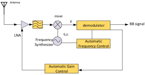
Architectures of reception systems
Figure 1.9 illustrates the most commonly used architecture at the reception level. Usually, the signal that the antenna detects does not contain only the information, it is often associated with noise and other unnecessary signals. Hence, a low-noise amplifier (LNA) and a band pass filter at the input of the receiver are used to reduce the noise level [9] [10]. After isolating the signal, it brought back to the same frequency allowing its treatment using a demodulator as shown in Figure 1.9. All the receivers are built around the same essential elements with different degree of complexity [10]. Antenna demodulator Automatic Frequency Control Automatic Gain Control Frequency Synthesizer mixer fLO if LNA BB signal
8
The received signal is demodulated, processed and transmitted to the destination. There are two main categories of receivers. The first type is homodynes receiver whose passes from the RF frequencies towards the low frequencies directly. The second type is the heterodyne receiver whose passes from the RF frequencies towards the lower frequencies in several stages.
1.3.1 Homodyne receivers (direct conversion or ZERO-IF)
The architecture of homodyne receivers is illustrated in Figure 1.10. The received RF signal is transposed directly into the baseband. The local oscillator (LO) signal is used to perform the transposition. The LO signal must be identical to the central frequency of the RF carrier signal, which will cancel the intermediate frequency IF. Then, the image signal is superimposed on the RF signal [9] [10].
The major disadvantage of this architecture is the presence of a DC offset voltage at the output of the mixers caused mainly by insulation faults at the mixer between the RF and LO channels. Moreover, the degradation of the sensitivity of the receiver to very low-frequency signals, because of the high level of noise that expressed in 1/f and non-thermal that will be superimposed on the wanted signal [10].
Despite these negative points, this type of receiver is increasingly popular because of the simplicity of RF processing which is associated with a much-improved level of integration compared to heterodyne receivers.
Antenna LNA 90 ° fLO = fRF I Q RF filter
9
1.3.2 Heterodyne receivers
This architecture consists of antenna, RF filter, low-noise amplifier, mixer, and the local isolator as shown in Figure 1.11. The principle work of the heterodyne receiver can be described as following, the transposition happening to the received RF signal around a fixed IF frequency. If this transposition is done in one-step, the receiver is called heterodyne. However, if it requires several steps, the receiver is called super heterodyne.
In the case of a super heterodyne structure, a first transposition of the spectrum can be achieved by multiplying the RF signal with the signal from a local oscillator fLO1. The second
transposition is performed by an I/Q demodulator consisting of a pair of mixers mounted in quadrature with a local oscillator fLO2. Because of its remarkable performance in terms of
selectivity, this architecture is the most used in second and third generation mobiles.
Antenna LNA 90 ° fLO = fRF I Q RF filter Image filter
fLO1
IF filter
Figure 1.11 Architectures of heterodyne receivers [10].
The major disadvantage of this receiver is related to the problem of image frequency rejection due to the several attempts have been made to integrate this structure. However, the RF and IF filters are difficult to integrate, which makes this architecture very cumbersome in terms of complexity. Effectively, the realization of these filters requires the integration of inductances to reach important quality factors, which is practically difficult, because of the quality factors that we can obtain are insufficient to ensure a good selectivity of the receiver [10].
10
1.3.3 Direct receiver (Demodulator)
The present of using the six-port to determine the phase of a high-frequency signal was early as 1964 [11]. The date of creation of the six-port as a measurement technique was reported in [12], and [13]. Although the authors have published partial ideas and used the term previously, these publications offer complete theoretical information as well as the approach for designing and optimize the six-port. The studies have continued to give more ideas that were fundamental as of the nineties of the last century [14]. Nowadays, researchers are more attracted to improve the multi-port performance due to the demands of the next generation technology. Besides, it has multiple usages as an analyzer [15] [16].
The general structure of the six-port shown in Figure 1.12 consists mainly of two inputs and four outputs. Each two of the four outputs are connected to a power detector. More details about six-port structure can be found in [9] [15] [16]. A set of characteristic equations can be used to find out the four unknowns. The six-port has a passive circuit comprised of couplers that are connected through transmission lines and phase shifters to produce linear signal outputs, combinations of phase shifted input signals, at I and Q the terminals. The six-port can be used as
a reflectometer to measure only the reflection coefficient and as network analyzer to measure the
Baseband recovery Power detector Power detector Baseband recovery + -+ -Six-port P1 RF P3 P4 P7 P2 P6 P5 Q I Antenna LO
11
transmission and reflection coefficients [10] [16]. The six-port junction was used successfully in the design of network analyzers [9], down-conversion, direct modulation, and more [10] [16].
The multi-port demodulator can be considered as homodyne type due to the direct conversion characterization. The block diagram of the multi-port demodulator shown in Figure 1.12. This multi-port demodulator described by three main blocks: six-port, power detection, and baseband recovery.
Multi-port correlator
At this step, a Local oscillator (LO) signal is combined with the modulated RF signal. As it shown by the six-port block diagram Figure 1.2, a shifted phase occurs between the combined signals RF (after the modulation) and LO in the six-port correlator. This phase shift depends on the S-parameters of the six-port correlator [9].
Power detection
In most cases, a Schottky diode power detector can be used for Power detection. The nonlinear characteristic of the Schottky diode is in a range of frequencies. In the Ideal power detector, a square law transfer function described in the equation below is used to model the power detector current as a function of the voltage [9].
IPD (v) = kv2
where k is a constant. (1.1)
Baseband Retrieving
Each output of the two diodes is connected to a differential baseband amplifier. In the amplifier stage, the output of each amplifier will be the difference between its inputs. Eventually, I / Q signals are retrieved in the last step.
Theory of Multi-Port Demodulator
The mathematical representation of demodulation as given in next formulas:
Z= ARF (XI + j XQ) e jωt (1.2)
g= ALO e jφ e jωt (1.3)
12
Z and ɡ are the modulated RF and LO signals respectively.
ω: is the angular frequency.
φ: is the relative phase between RF and LO.
ALO: LO amplitude.
ARF: RF amplitude.
XI and XQ: are the transmitted baseband I and Q data.
RF and LO are combined as:
y = Sx2g + Sx1z (1.4)
Where x coincides to one of the four output ports P1 – P4, x ϶ {1, 2, 3, 4}. Snm is the
S-parameter transmitted from port m to port n of the multi-port correlator [9]. Since, a1 = z is the RF wave on port P6 and a2 = g on port P5. An ideal power detector modulation with a square law transfer function considered as:
𝑌𝑥= 𝑅 {𝑦𝑥} = y𝑥 + y𝑥
2 (1.5)
The above formula used to calculate real part (time-domain) signal. Then, by squaring the result the real part (time-domain) output voltage Vx is as shown next:
𝑉𝑥 = 𝐿𝑃𝐹 {𝑘𝑌𝑥2} = 𝑘 𝑦𝑥 𝑦𝑥
2 = 𝑘
|𝑦𝑥|2
2 (1.6)
Solving (1.2) and (1.6) by using Euler’s formula where (k=1) 𝑉𝑥 becomes:
𝑉𝑥= |𝑆𝑥2|2 𝐴𝐿𝑂2 ⁄ + |𝑆2 𝑥1|2 𝐴𝑅𝐹2 (𝑋𝐼2+ 𝑋𝑄2) 2⁄ + (1.7)
𝐴𝐿𝑂 𝐴𝑅𝐹 |𝑆𝑥| 𝑋𝐼 cos(𝜙 + ∠𝑆𝑖) +
𝐴𝐿𝑂 𝐴𝑅𝐹 |𝑆𝑥| 𝑋𝑄 sin(𝜙 + ∠𝑆𝑖)
where, |𝑆𝑥| = |𝑆𝑥1||𝑆𝑥2| (1.8)
∠𝑆𝑥= ∠𝑆𝑥2− ∠𝑆𝑥1 (1.9)
From (1.7), the presence of XI and XQ in the output signal Vx is a different phase ɸ of RF and
LO as well as how the phase and the gain are correlating in the multi-port.
13 𝑆 =1 2 [ 0 0 −1 𝑗 −1 𝑗 0 0 1 𝑗 𝑗 −1 −1 1 0 0 0 0 𝑗 𝑗 0 0 0 0 −1 𝑗 0 0 0 0 𝑗 −1 0 0 0 0 ] (1.10)
The following formula is the mathematical representation of the detection of 𝑄 (𝑄𝑑), and 𝐼 (𝐼𝑑)
signals - For the derivation of these equations refer to [9] - as:
𝐼𝑑= 2 𝐴𝐿𝑂 𝐴𝑅𝐹 (𝑉4− 𝑉3) (1.11) 𝑄𝑑 = 2 𝐴𝐿𝑂 𝐴𝑅𝐹 (𝑉6− 𝑉5)
In the ideal case of detection, the received 𝐼𝑑and 𝑄𝑑signal should be same as the transmitted
𝐼 and 𝑄 signal (𝐼𝑑= k XI and 𝑄𝑑= k XQ) since k is a scaling factor. In the real case of the multi-port
correlator there might be a phase and/or amplitude imbalance, thus, unwanted transfer between the two channels (𝐼 and 𝑄).
The differences between the multi-port receiver and the conventional receiver could be concluded in terms of advantages and disadvantages. The multi-port receiver has higher bandwidth and higher data rate. Also, higher linearity and low loss because of its passive circuit. Moreover, it has lower power detection and better correlation due to its distributed circuit. On the other hand, it has low sensitivity and the limitation in the dynamic range due to the use of the diode detectors. Second is the size concern, this because of the multi-port correlator is a distributed circuit [9].
Millimeter wave demodulator
Nowadays, studies and measurements demonstrate that 5G mm Wave could be a significant member of 5G technology [5] [6]. However, in the past mm Wave bands mostly used for cell phone services because of the concerning short-range and non-line of sight coverage matters.
The advanced technology is promising to solve the preventions of using mm Wave bands for mobile. The short transmission paths and high propagation losses can be improved by the reuse of the spectrum in microcellular propagation and by the reduction in interference between the close cells. Besides, the tiny antennas -because of mm Waves signals- for concentrating signals with a significant gain can compensate for propagation losses. Moreover, the characteristic of the short wavelength for mm Wave gives a possibility to build up what so called multi-element
14
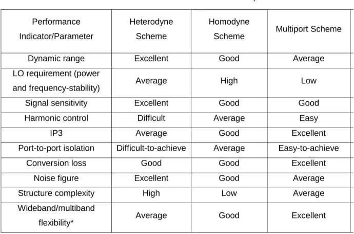
dynamic beam-forming antennas. These will be a small enough in size to install into handsets where cannot be done in the wavelength frequencies less than 6 GHz which is nowadays the operation frequencies for phones [6]. Also, mm Wave frequency bands are useful in areas that require such capacity by supporting very high capacity networks. In addition, the use for the backhaul and the machine-to-machine communication. Meanwhile, the 5G technology latency promising to allow variation of the Internet of Things (IoT) applications such as fitness and healthcare devices, autonomous driving cars, wearables, home, and office automation, etc. [6]. Table 1.2 is showing the performance Indicator/Parameter for different types of mm Wave receivers as well as a comparison between them.
Although heterodyne receiver can reach the 100 dB of dynamic range, it requires a mixer for bring the RF and IF modulated signals together. Homodyne receiver is using quadrature down-conversion resulting in obtaining the maximum information from modulated I/Q signal. However, the multi-port is limited in this term because of the limit of the quadrature region of the used diodes.
Table 1.2 Performance comparison of heterodyne, homodyne and multiport techniques (with reference to diode-based receiver architectures)
Performance Indicator/Parameter
Heterodyne Scheme
Homodyne
Scheme Multiport Scheme
Dynamic range Excellent Good Average
LO requirement (power
and frequency-stability) Average High Low
Signal sensitivity Excellent Good Good
Harmonic control Difficult Average Easy
IP3 Average Good Excellent
Port-to-port isolation Difficult-to-achieve Average Easy-to-achieve
Conversion loss Good Good Excellent
Noise figure Excellent Good Average
Structure complexity High Low Average
Wideband/multiband
flexibility* Average Good Excellent
*This is a special design consideration for certain special applications such as software-defined radio, UWB etc. [11].
15
The LO used in the Homodyne and heterodyne receivers should satisfy some requirement in term of power (5 to 10 dB). At mm Wave, it is complicated to add an amplifier to reach the required power. The multi-port does not require high LO power, which the advantage here thus reduces the consumption of the DC at the level of the receiver. Hence, this can be one way to solve the DC problem.
Proposed work
In most cases, the multiport demodulator offers low complexity and low-cost measurements [12] [13] [14]. However, from the block diagram Figure 1.12, the two inputs are located into both sides of the multiport. Nevertheless, the proposed arrangement of the multi-port aiming to arrange the inputs in one side and the outputs in one side separately with considering the size reduction.
The Beamforming Networks as Butler and Nolen have been presented and discussed in many of works recently and before more details can be found in [15] [16]. Considering them as a useful tool and suitable configuration to have the required arrangement where the input ports are on one side and the output port on the other side. Moreover, the amplitude and phase arrangement should be modified to follow the rules that defined by the six-port.
Momentum technology development has a significant impact on mm Wave bands and 5G technology services. Some providers decided to make a forward step by making strategy and started tackling the challenges to develop 5G services. As this work, focus on the design of mm Wave demodulator based on Nolen Matrix for the 5G Application.
Frequency selection
The academic researchers have more interest in the 28 GHz band where ensuring to apply the high data-rate applications, with suitable bandwidth, in this band [6]. However, In Canada ISED allowed equipment experiments by innovators to study the new services such as sensing equipment, video transmission utilizing non-conventional frequencies, and mobile systems within mm Wave spectrum bands. Moreover, ISED will continue to allow flexible studies at 28 GHz band; however, it will remain to support an ongoing development for 5G technology [5]. Noticeably, the 5G technology has an interest in different frequencies. Hence, this work is concerning mm Wave band around the 28 GHz frequency.
17
2
CHAPTER TWO: Design of Nolen Matrix
Multi-port beamforming
Beamforming network (BFN) is playing the main role in building intelligent antenna systems. In BFN, N antenna elements connected to M beam ports to form the multiple beams. Conventional beam orientation can be achieved by adjusting only the phase signals of the different elements. A phase distribution should be accomplished to direct the beam in the desired direction. BFNs are ingenious devices comprising circuits formed of directional couplers and phase shifters. By connecting a BFN to the antenna array and RF switches, a set of beams can be realized by exciting one or more ports simultaneously by RF signals. A signal presented at an input port will produce equal excitations at all ports with a gradual phase shift between them, resulting in a beam that radiates in a specific direction of space. A signal at another input port will form a beam in another direction [23]. Several beamforming techniques can provide fixed beams: matrices as Butler, Blass, and Nolen and lenses as Rotman or Luneberg. The Butler matrix is the most widely used because of its ease of design [24].
The BFN, for example, is one of the key components in multiple input multiple output (MIMO) system. MIMO technique is one of the most attractive candidates for increasing spectrum efficiency since it significantly increases the throughput and reliability without additional bandwidth when applied to the radio frequency path.
BFN matrices
In this section, we are going to review BFN matrices to explain the work principle of each.
2.2.1 Butler matrix
The most cited matrix for the formation of a beam supply network is probably the Butler matrix. A reciprocal and symmetrical passive circuit with N input ports and N output ports drives where N radiating elements producing N different beams. Figure 2.1 shows a diagram of a 4x4 Butler matrix.
The standard form of the matrix when N must be an integer power of 2 (N = 2n where n is a
positive integer). For forming the conventional network, couplers (3 dB, 90°) with 0 dB couplers (which can be realized by the combination of two 3 dB couplers) are used. The non-binary form is recognized using a combination of prime numbers of ports: 3x3, 5x5, 7x7, and so on. Note, for non-binary structures that the couplers are no longer limited to hybrids (3 dB, 90°). The formation
18
of multiple beams is possible, with some limitations. Two adjacent beams cannot be formed simultaneously because they add up and produce a single beam. Moreover, Butler matrix is considered the most interesting option because of its ability to form orthogonal lobes and the simplicity of its design. Compared with its counterparts Blass and Nolen, the Butler matrix requires fewer couplers (for a 4x4 matrix as shown in Figure 2.1, four couplers are needed for the Butler matrix, 6 couplers for Nolen and 16 for Blass). The Butler matrix is a parallel system, unlike the Blass matrix (serial system).
The design of large matrices is quite easy since the phase shifters can be placed symmetrically with respect to the phase line and subsequently the diagram of Butler matrix is identical to that of an FFT (Fast Fourier Transform). Where Butler matrix consists of three basic elements:
H: hybrid couplers or junctions:
H = N
2 log(N) (2.1)
P: fixed phase shifters generally delay lines:
P = N 2 (log(N) − 1) (2.2) C: crossing: C = ∑ [N 2(2 k−1− 1)] log2(N) k− (2.3) -45° -45° 1R 2L 2R 1L
19
For a large matrix (many crossings, for example, 16 crossings are necessary for an 8x8 matrix, for a matrix with 32 ports, one will need 416 crossings). This could introduce higher levels of transmission loss [23].
2.2.2 Blass matrix
coupler θ0 θ1 θ2 θ3 θ4 θ5 . θ36 Loads Network of N sources secondary lines main linesFigure 2.2 Topology of Bless matrix.
The Blass matrix is a serial power network with a lattice structure like that shown in Figure 2.2 [25] [26]. The matrix has several transverse lines (through lines) that carry the energy and several branch lines that intersect the first and lead to the network. Couplers are placed at each crossing so that a fraction of the energy incident on the main line directed at a second line in a definite direction. The other end of the second line provided with an absorbent charge. Between two directional couplers, a phase shifter or line-length adjuster generates the phase change required to create the phase gradient between each output port. The coupling coefficients of the different couplers and the phase shift values of the different constant or variable phase shifters are calculated to obtain the diagrams of desired energy that are different depending on whether power is coming in or being taken by one or the other of the main lines.
The Blass matrix widely used despite it is expensive and complicated because of the particular directional couplers that must be provided at each crossing. The Blass matrix can be designed regarding use with any number of elements. However, there are significant losses because of the loads at the terminals [23].
20
2.2.3 Nolen Matrix
Nolen matrix can be considered as a special case of the Blass matrix where N antennas are coupled to M beam ports. Thus, Nolen matrix can feed a number of antennas different from the number of beam orientations. This matrix consists of two types of components (coupler and phase shifter) and does not show any crossover [23]. Each node in the matrix consists of a directional coupler of parameter θij and a phase shifter of parameter φij. Mosca algorithm used to calculate
these parameters from N and M and the direction of the beams [27]. Figure 2.3 shows 2 x N Nolen matrix, the coupler/phase shifter with specific θij, φij placed in two rows with specific arraignment
between the two inputs and the four outputs to assure the multi-port theory of working.
b1 b2 bj ………. bN-1 bN a1 a2 ɸ ij (1) (2) (3) (4) θij bij aij b(j+1) a(j+1)
Figure 2.3 The general form of the Nolen matrix. [16]
Nolen matrix as demodulator
Nolen matrix is more adapted to build a structure like six-port with two inputs and four outputs matrix. Unlike Butler matrix, which gives 4 x 4 (since two ports are unusable at this case) and Blass matrix, which require, load with less efficiency because of the losses at the loads as it described previously in Blass matrix section. Moreover, the advantage of no crossover exist in this technique unlike to Blass matrix technique.
21
2.3.1 Six port demodulator
The demodulation chain was implemented by Agilent's ADS software. Figure 2.4 provides an overall scheme diagram done by ADS software simulation of direct conversion six-port using the ideal components.
Figure 2.4 A diagram showing the ADS simulation of the multi-port direct conversion with ideal six-port.
The modulated input signal QPSK passes into a block containing the multi-port dispersions S-parameter behavior. At the multi-port outputs, power detectors are placed using ideal components. I/Q information of the QPSK demodulated with differential amplifiers for baseband recovery (see Figure 2.5). This subtraction assembly makes it possible to perform the subtraction of the signals in addition to minimize the undesired DC component.
22
Figure 2.6 shows the input and output signals in the range of 0 to 1 μs. From the same figure, it is clear that the output signals Iout / Qout are containing the same information of the input signals
Iin / Qin respectively. It is noticeable that the multi-port brings little distortion in the recovered
signals. A slight variation in voltage amplitude can be noticed.
Figure 2.7 illustrates the spectrum of the QPSK modulated input signal. It is noticeable that the width of the spectrum which corresponds to a signal of 100 Mb/s. The Figure 2.8 shows, in addition to the LO input signal, the spectrum of output signals Iout/Qout where both are having the same width of the spectrum which corresponds to a signal of 100 Mb / s.
(a)
(b)
Figure 2.6 Input and output signals (a) Iinput/Ioutput in volt vs. time and (b) Qinput/Qoutput in volt vs. time.
23 A m p li tu d e , d B m Frequency, MHz
Figure 2.7 Spectrum of the input QPSK modulated signal.
Qout Iout A m p li tu d e , d B m Frequency, MHz Vin
Figure 2.8 Spectrum of the QPSK demodulated signals (Iout and Qout) at the output and the input LO signal (Vin).
24
Design of Nolen matrix (using ideal components)
The theoretical parameters of the directional couplers and phase shifters associated to the Nolen matrix obtained for the matrix described above are reported in Table 2.1. These values indicate that three different directional couplers and different phase shifters are necessary to build the equivalent six-port Nolen matrix.
Building the receiver system, starting from building the Nolen matrix system using ADS software. Nolen matrix built up with ideal components as shown in Figure 2.9. The coupler within
Table 2.1 Parameters of the Nolen 2X4 Matrix Retained (θij andɸij) [23]
1 2 3 4 1 0.500 00 0.500 00 0.707 00 1.000 00 2 0.577 00 0.500 1800 1.000 00
25
gain balance (showing as “GainBal” in Figure 2.9) of 0 dB corresponds to the 3 dB one, the coupler within gain balance of 3.01 dB corresponds to the 4.7 dB one, and the coupler within gain balance of 4.77 dB corresponds to the 6 dB one. Figure 2.10 evaluates the results of Nolen matrix (using ideal components) and illustrates the simulated relative phase differences between adjacent output ports for port1 and adjacent output ports for port6. The input ports are defined as port 1 and 6 to conserve the same nomination used for the six-port as well as in equation 1.10
(a)
(b)
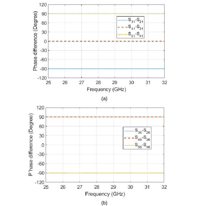
Figure 2.10 Simulated relative phase differences between (a) adjacent output ports for port1, and (b) adjacent output ports for port 6.
26
and port 2 to 5 are the output ports. Two loads were added to the 3 dB and 4.7 dB couplers respectively.
The potential to use the Nolen matrix as a demodulator is showing in Figure 2.10. This figure shows the phase difference between two adjacent output ports when port 1 is used as an input Figure 2.10 (a) and when the port 6 is used as an input Figure 2.10 (b). The phase distribution fellow the same distribution as the six-port defined by matrix in the equation 1.10.
Six port based on Nolen matrix with ideal components
To verify the feasibility to use the proposed Nolen Matrix as a demodulator, a building block diagram replaces the six-port (in Figure 2.4) in Figure 2.11. An ADS simulation showing the direct conversion receiver based on Nolen matrix with ideal components.
Figure 2.11 Six port based on Nolen matrix using ideal components.
Figure 2.12 shows the input and output signals in the range of 0 to 1 μs. From this figure, it is clear that the signals of the input QPSK modulation Iinput / Qinput are in phase with the output
signals Iout / Qout respectively. It is noticeable the distortion in the recovered signals, a slight
27 V o lt a g e ( V ) Time (us) Iout Iin (a) V o lt a g e ( V ) Time (us) Qout Qin (b)
Figure 2.12 Input and output signals (a) Iinput/Ioutput in volt vs. time and (b) Qinput/Qoutput in volt vs. time.
Figures 2.13 and 2.14 are showing the spectrum of the input/output QPSK modulated/demodulated signals respectively. A good agreement has been shown between both signals input modulated and output demodulated QPSK, having an almost same specification, with the previous Figures 2.7 and 2.8 before applying the Nolen matrix.
28 Am p li tu d e , d B m Frequency, MHz
Figure 2.13 Spectrum of the input QPSK modulated signal. Iout Am p li tu d e , d B m Frequency, GHz Qout Vin
Figure 2.14 Spectrum of the output QPSK demodulated signals (Iout and Qout) and the input signal (Vin).
29
3
CHAPTER THREE: Building Multi-Port System
In this chapter, three design steps are presented: couplers, phase shifter, and the multi-port. Three different hybrid couplers 3, 4.7, and 6 dB were discussed and designed. Moreover, a review is given about state of the art of phase shifter to introduce the proposed double T-shape phase shifter. The new proposed double T-shape phase shifter is discussed and designed using ADS software. Lastly, the multi-port based on Nolen matrix was designed.
Directional coupler
Hybrid couplers (or Branch line) are passive devices widely used in the microwave and RF circuits. What coupler is doing is coupling a portion of signal in the transmission line to the port enabling this signal to be used in different circuits.
Transmission port P2 Input port P1 Isolated port P4 Coupled port P3
Figure 3.1 Single section 3 dB Hybrid couplers 90 °.
The branch line is the simplest type of quadrature coupler since the circuitry is entirely planar. An ideal single-box branch line coupler is shown in Figure 3.1 where each transmission line is a quarter wavelength. Branch line couplers are very easy to design and sufficient to use for some applications due to their ideal performance at the central frequency desired.
Double-box branchIines
The S parameter matrix of the symmetric coupler given by [28]:
[𝑺] =√21 | 0 1 𝑗 0 1 0 0 𝑗 𝑗 0 0 1 0 𝑗 1 0 | (3.1)
30
The configuration of the designed hybrid coupler shown in Figure 3.2 is branch line version proposed in [29]. This version offers improved performance in terms of bandwidth and isolation and coupling ratio compared to the standard branchline coupler. The coupler has been optimized by modifying the dimensions and the coupling gape. All the three section lines used to define the coupler are a quarter wave. This is due to the quarter wavelength line (λ / 4) between the output ports. The impedance distribution defines the coupling ratio.
All the three coming hybrid couplers (3dB, 4.7dB, and 6dB) are following the same design procedure.
3.2.1 Hybrid coupler (3dB, 90 °)
The overall size of the coupler is (7.278 × 3.268 mm2), and the used substrate is
(Rogers_RT_Duroid6002) with a permittivity of 2.93 and a thickness of 0.254 mm. The coupler has been designed to operate in "broadband" mode (25 - 32 GHz).
Figure 3.4 show two sectors of the quarter-wavelength line, which form the structure of the coupler between ports 1 and 4, and between ports 2 and 3. We have a quarter wave line of characteristic impedance Zo equivalent to that of the input and output ports of the coupler. On the
other hand, between ports 1 and 2 and between ports 3 and 4, we have us quarter-wavelength line with a characteristic impedance of Zo/√2 to obtain a coupling of 3dB.
Figure 3.5 shows the simulated S-parameter results. A very good isolation and matching were obtained with S11 values of under -24 dB for the bandwidth. Moreover, the transmission
coefficient is 3 dB at port 2 (S21) and port 3 (S31), which indicates that very low unbalance
between the two output port.
Z1 Z2 Z1 Z2 Z3 Zo=50 Ω Zo=50 Ω Zo=50 Ω Zo=50 Ω P1 P4 P3 P2
31
Figure 3.3 Simulation of Hybrid coupler (3dB, 90 °) in ADS.
44.44 Ω 106.69 Ω 53.43 Ω 50 Ω 50 Ω 50 Ω 50 Ω P1 P4 P3 P2 3.01 mm 0.77 mm 1.86 mm 0.57 mm 106.69 Ω 0.14 mm 44.44 Ω
Figure 3.4 The Layout of the Hybrid coupler 3dB showing details about dimensions in (mm) and impedance in (Ohm).
32
3.2.2 Hybrid coupler (4.7dB, 90 °)
The overall size of the designed 4.7 dB coupler is (6.696 × 3.5093 mm2) with the used
substrate (Rogers_RT_Duroid6002). Figure 3.7 is giving more details about the designed, dimensions (millimeter), and the impedance (Ohm) of the optimized 4.7dB coupler.
Figure 3.8 is a plot of the simulated S-parameters (Amplitude). The results for both isolation and matching are showing better than 20 dB for the band from 25.8 GHz to 32 GHz. In this bandwidth, the coupling is changing from to 4.6 dB to 5.2 dB delivering un unbalance of ±0.3dB.
Figure 3.6 Simulation circuit of Hybrid coupler (4.7dB, 90 °) in ADS.
44.44 Ω 86.17 Ω 44.9 Ω 50 Ω 50 Ω 50 Ω 50 Ω P1 P4 P3 P2 3.08 mm 0.77 mm 1.86mm 0.76mm 86.17 Ω 0.24mm 44.44 Ω
Figure 3.7 The Layout of the Hybrid coupler 4.7 dB showing details about dimensions in (mm) and impedance in (Ohm).
33
Figure 3.8 The simulated results showing S parameter of coupler 4.7 dB.
3.2.3 Hybrid coupler (6 dB, 90 °)
The overall size of the coupler is (6.74926 × 3.438 mm2) with the same substrate
(Rogers_RT_Duroid6002). The layout of the hybrid coupler is shown in Figure 3.10 with more details about the dimensions (in millimeter), and the impedance (in Ohm) of the 6dB coupler.
Figure 3.9 Simulation circuit of Hybrid coupler (6 dB, 90 °) in ADS
Figure 3.11 is a plot of the simulated S-parameters (Amplitude). The results for both isolation and matching are showing better than 20 dB for the band from 26.5 GHz to 31.5 GHz. Moreover, the transmission coefficient is of 6 dB for S21 at port 2 (S21) and about 2 dB for S31 port 3 (S31).
34 25.54 Ω 77.94 Ω 36.89 Ω 50 Ω 50 Ω 50 Ω 50 Ω P3 P2 2.94 mm 0.77 mm 1.88 mm 1.01 mm 77.94 Ω 0.29 mm 25.54 Ω P1 P4
Figure 3.10 The layout of 6 dB hybrid coupler showing details about dimensions in (mm) and impedance in (Ohm).
Figure 3.11 The simulated results showing S parameter of coupler 6 dB.
Phase shifter
Phase shifters are used for changing the phase angle of the two-port transmission line (S21).
The phase shifter should show a low insertion loss in all phase states, the equal amplitude for all providing a flat phase versus frequency within the desired bandwidth. Besides, the designed circuit should also satisfy the requirement of limited area.
3.3.1 Schiffman phase shifter
A constant input resistance 90° type phase shifter for larger bandwidths was described in [30] by Schiffman. An amplitude balance and broadband phase can be fulfilled by using several arrangements [31]. Figure 3.11 shows the general configuration of Schiffman Phase shifter [30] that has been used for a wide verity of applications playing the main role component in
35
beamforming [31][32]. Schiffman phase shifter consists of two transmission lines. One line is bent over (coupled line) for dispersivation with of quarter wavelength and one line as a reference of three-quarters wavelength as is shown in Figure 3.12. A near constant phase difference can be achieved when considering a certain line length and coupling degree along broadbandwidth frequency. Schiffman demonstrated that the phase difference between quarter wavelength line and three-quarters wavelength is 90 0. The two equations (3.2) and (3.3) given below are
describing the image impedance 𝑍𝐼, and phase constant 𝛷 respectively for Schiffman phase
shifter [30]. Figure 3.13 is showing the connection of the coupled lines and their even and odd modes characteristic impedances of the lines and their length.
𝑍
𝐼= √𝑍
0𝑜𝑍
0𝑒,
(3.2) 𝑍𝐼 : Image impedance.𝑐𝑜𝑠 𝛷 =
𝑍0𝑒 𝑍0𝑜−𝑡𝑎𝑛 2𝜃 𝑍0𝑒 𝑍0𝑜+𝑡𝑎𝑛2𝜃 , (3.3)𝛷: Phase constant.
𝜃: is the electrical length of a uniform line length L and phase constant P.
1 2 3 4 V 3λ/4 V e jɸa V ejɸb λ/4 Z0 e Z0 o V
Figure 3.12 The Standard structure of 900 Schiffman phase shifter.
Figure 3.12 illustrates the basic Schiffman phase shifter principle work according to equations 3.2 and 3.3.
36
Figure 3.13 Coupled-transmission-line element with ends connected and curves of its phase response for three values of (ρ =𝑍0𝑒⁄𝑍0𝑜) [30].
3.3.2 Modified Schiffman phase shifter
Figure 3.14, designs worked on Schiffman Phase shifter toward larger bandwidth and accuracy [29]. This work use different configurations of transmission lines (Figures b, c, and d) to have more flexibility in term of the dimension (coupling space) defined by the coupling degree (ρ =𝑍0𝑒⁄𝑍0𝑜). Kθ (a) θ , ρ θ2 , ρ2 θ1 , ρ1 Kθ θ1 , ρ1 θ2 , ρ2 θ2 , ρ2 θ1 , ρ1 Kθ (b) (c) (d)
Figure 3.14 Some alternatives to obtain a differential phase shifter: (a) Standard Schiffman phase shifter, (b) Double Schiffman phase shifter, (c) Schiffman phase shifter with cascaded sections, and (d)
Parallel Schiffman phase shifter [33].
Others modified Schiffman phase shifter based on improving the wide-band by increasing the even mode when the ground plane under the coupled lines removed. Vice Versa, reducing the odd mode when an additional rectangular conductor is applied [32].
37
Figure 3.15 A 900 Schiffman phase shifter layout using a patterned ground plane [32].
Based on the above details, the previous shapes of phase shifter cannot be compatible with the proposed circuit of this thesis both bandwidth and spacing problem. The distance between the two lines of the phase shifter is defined by the distance between the two input ports of the coupler. In this section, we propose miniaturized phase shifter (see Figure 3.16) that works well in terms of the desired bandwidth and the limited space of the circuit.
3.3.3 Double T - shape phase shifter
In the review of Schiffman's phase shifter and to the modifications that were added to it. The phase shifter that proposed here is designed to reduce the area used and to maintain the quality as of phase shifting with high performance. A substrate form simulated, designed and fabricated for the proposed design double T-shape phase shifter.
This newly proposed structure tackles
the limited spacing problem and is integerable with designed couplers in the desired
circuit. Where here, a study has been made to bend the two sides of modified Schiffman
shifter.
3.3.4 Double T-shape phase shifter 90
0This technique employs the proposed double T-shape, which is different of the conventional designs as is shown by the general shape in Figure 3.16. Because this method mainly aimed for reducing the size, it can be useful for many applications when the limitation of the area is the concern, especially when working in mm Wave bands where circuits are very small. It is worth mentioning that, both top and bottom T-Shapes are symmetrical for each element of the phase shifter (see Figure 3.16). The top one T-Shape element dimensions: the width of coupled lines set at 0.08 mm for entire the element, and the coupled lines gape set at 0.20 mm in the horizontal
38
plane and 0.16 mm in the vertical plane (with considering the symmetry for each element). For the bottom element the dimensions: the width of coupled lines set at 0.10 mm for entire the element, and the coupled lines gape set at 0.07 mm in the horizontal plane and 0.17 mm in the vertical plane (with considering the symmetry for each element).
The results plotted in figures show a very good phase shifting over the proposed broadband width frequencies of roughly (900 ± 20) around the desired frequency (28 GHz). Showing significant
results for a bandwidth (7.75 GHz) from 26.25 GHz to 34 GHz. Moreover, the achievement of acceptable results in terms of the reflection coefficient (S11≈ -13 dB) for the entire bandwidth.
Z 0= 50Ω 0.08 mm 0.16 mm 0.17 mm 0.20 mm 0.10 mm 0.07 mm Reference line Z0 = 50Ω Z0 = 50Ω Z0 = 50Ω
Figure 3.16 The layout of the proposed 90° double parallel double T-shape phase shifter with considering the symmetry for each element.
39 (a)
(b)
Figure 3.17 Simulated results of the proposed 90 T-phase shifter. (a) Amplitude response. (b) Phase response.
Designed Nolen matrix using ADS
Nolen matrix based on a conventional network topology is designed at the center frequency of 28 GHz with roughly 5 GHz bandwidth. The designed branch line couplers have a phase shift of 90°, so this point must be taken into the consideration. An optimization step was done. As it is expected theoretically, a phase deferent can be a problem due to a deferent transmission lines length.
40
The proposed solution is a Nolen matrix where the different paths must be aligned as much as possible to increase the bandwidth. An almost parallel architecture is used in this matrix. Compensation of the delay generated by the couplers will ensure broadband behavior. This matrix has an advantage in terms of its performance that can be comparable to Butler matrix with the possibility of designing matrices with any N x M combination besides to the main advantage of separating the inputs and output.
Figure 3.18 shows the simulated layout from Momentum (ADS). Equal transmission lines are added to the initial design to discrete the input access as well as the output to facilitate the characterization and to compensate the phase difference.
Figure 3.29 is showing the energy distribution and the isolation when the excitation applied to the input ports (P1 and P6) one each time. First, P1 is excited to show the energy distribution in the four output ports (P2, P3, P4, and P5) where the other input ports P6, P7, and P8 (P7 and P8 are unused ports) were isolated. The last step was repeated for the other input port P6 to show the energy distribution in the four output ports (P2, P3, P4, and P5) where the other input port P1
P1 P2 P3 P4 P5 P6 Phase shifting A B C A: 6dB coupler B: 4.7dB coupler C: 3dB coupler C B P8 P7
41
was isolated and the unused two ports P7, and P8 were isolated as well. A good isolation can be noticed and normal distribution by applying this technique.
(a)
(b)
![Figure 1.3 Current Canadian band plan in the frequency band 27.5-28.35 GHz [5].](https://thumb-eu.123doks.com/thumbv2/123doknet/5004764.124711/20.918.122.797.418.609/figure-current-canadian-band-plan-frequency-band-ghz.webp)
![Figure 1.5 Current use of the frequency band 37-40 GHz by fixed service [5].](https://thumb-eu.123doks.com/thumbv2/123doknet/5004764.124711/21.918.125.809.404.658/figure-current-use-frequency-band-ghz-fixed-service.webp)
![Figure 1.10 Architectures of homodyne receivers [10].](https://thumb-eu.123doks.com/thumbv2/123doknet/5004764.124711/24.918.99.805.668.1001/figure-architectures-homodyne-receivers.webp)
![Figure 1.11 Architectures of heterodyne receivers [10].](https://thumb-eu.123doks.com/thumbv2/123doknet/5004764.124711/25.918.148.806.466.775/figure-architectures-heterodyne-receivers.webp)
![Figure 2.3 The general form of the Nolen matrix. [16]](https://thumb-eu.123doks.com/thumbv2/123doknet/5004764.124711/36.918.163.764.400.761/figure-general-form-nolen-matrix.webp)