HAL Id: tel-03222180
https://tel.archives-ouvertes.fr/tel-03222180
Submitted on 10 May 2021HAL is a multi-disciplinary open access archive for the deposit and dissemination of sci-entific research documents, whether they are pub-lished or not. The documents may come from teaching and research institutions in France or abroad, or from public or private research centers.
L’archive ouverte pluridisciplinaire HAL, est destinée au dépôt et à la diffusion de documents scientifiques de niveau recherche, publiés ou non, émanant des établissements d’enseignement et de recherche français ou étrangers, des laboratoires publics ou privés.
Emerging Technology for RF and Millimeter-wave
Circuits based on Carbone Nanotubes
Phi Long Doan
To cite this version:
Phi Long Doan. Emerging Technology for RF and Millimeter-wave Circuits based on Carbone Nan-otubes. Micro and nanotechnologies/Microelectronics. Université Grenoble Alpes [2020-..], 2020. English. �NNT : 2020GRALT080�. �tel-03222180�
THÈSE
Pour obtenir le grade de
DOCTEUR DE L’UNIVERSITE GRENOBLE ALPES
Spécialité : Optique et RadiofréquenceArrêté ministériel : 25 mai 2016
Présentée par
Phi Long DOAN
Thèse dirigée par Florence PODEVIN, Maître de conférence, Université Grenoble-Alpes-Grenoble INP, et
codirigée par Emmanuel PISTONO, Maître de conférence, Université Grenoble-Alpes
préparée au sein du Laboratoire RFIC-Lab dans l'École Doctorale E.E.A.T.S
Technologie émergente pour le
développement de circuits RF et
millimétriques à base de
nanotubes de carbone
Thèse soutenue publiquement le 17 Décembre 2020, devant le jury composé de :
M. Didier VINCENT
Professeur à l’Université Jean Monnet de Saint-Etienne, Président M. Frédéric ANIEL
Professeur à l’Université de Paris-Saclay, Rapporteur M. Anthony GHIOTTO
Maître de conférence à Bordeaux-INP, Rapporteur Mme. Marjorie GRZESKOWIAK
Maître de conférence à l’ISAE-Supaero, Examinatrice M. Dominique BAILLARGEAT
Professeur à l’Université de Limoges, Examinateur M. Philippe COQUET
Professeur à l’Université de Lille, Examinateur Mme. Florence PODEVIN
Maître de conférence à l’Université Grenoble-Alpes--Grenoble-INP, Directrice de thèse M. Emmanuel PISTONO
1
Acknowledgments
First and foremost, I would like to express my appreciation and sincere gratitude to my supervisor, Mrs. Florence PODEVIN and my co-supervisor, Mr. Emmanuel PISTONO for their unconditional help, support and guidance that have instructed me all along my work in this PhD thesis. Without their precious advices and valuable comments, this thesis would not be achieved. I would also like to express my thanks to Prof. Philippe FERRARI for giving the opportunity to commence this 3-year interesting and unforgettable journey. During these years, I have learnt from many people not only how to work in a scientific way, but also how to improve myself day by day.
Besides my advisors, I would like to thank the rest of my thesis committee: Prof. Frédéric ANIEL from University of Paris-Saclay, and Mr. Anthony GHIOTTO from Bordeaux-INP for having accepted to review this thesis; Mrs. Marjorie GRZESKOWIAK from ISAE-Supaero, Prof. Philippe COQUET from University of Lille and Prof. Dominique BAILLARGEAT from University of Limoges for examining this work and Prof. Didier VINCENT from University of Saint-Etienne for being the president of my thesis jury.
I would also like to acknowledge the ANR TRICOT project for financing me during this thesis period. In the same framework, I would express my sincerest thanks to our collaborators in this project: Prof. Dominique BAILLARGEAT, Mr. Kamel FRIGUI, Mr. Stéphane BILA, Mr. Philippe ROUX-LEVY and Mr. Joseph DE-SAXCE from XLIM laboratory, Limoges, France for their sharing experiences in carbon nanotubes modelling; Prof. Philippe COQUET, Mr. Jianxiong WANG, Mr. Siah CHUN FEI, Mr. Simon GOH CHUN KIAT from CINTRA laboratory, Singapore; Mr. Stéphane PIOTROWICZ from III-V Laboratory, Paris, France for their helps in sample preparations and fabrications that was performed in this thesis. Especially, I would like to thank the XLIM laboratory for accommodating me during my research period at University of Limoges, France.
I wish to extend my special thanks to the technical team, Mr. Nicolas CORRAO and Mr. Loïc VINCENT for their useful guideline and their endurance patience when helping me to carry out hundreds measurements with always a smile on their faces.
I would alsos like to show my deep appreciation to the administrative and technical office of RFIC-Lab, Mr. Frédéric CHEVROT, Mr. Ahmed KHALID, Mr. Youness RAJAB, Mrs. Anne-Laure FOURNERET and Mrs. Laurence BEN-TITO for their valuable help and support during this thesis.
A very special gratitude goes to my fellow labmates and friends in RFIC-Lab: Marc, Jordan, Giuseppe, Anh Tu, Julio, Leonardo, Mohamad, Imadeddine and so on. I am very grateful to work with you all.
Last but not least, nobody has been more important to me in this tough adventure than the members of my family. I would like to thank my parents Phi Phong DOAN and Thi Hoa BUI, my younger sister Bui Thao Ngan DOAN, whose unlimited love, guidance and support always are with me in whatever I pursue. More importantly, I would like to thank my loving and supportive wife, Nhu Quynh, who always stays beside me to share the difficulties of life and boosts me up when I was exhausted during this thesis. Without you, this hard work could not be completed at all.
2
Abstract
The fifth-generation (5G) technology is known as the new generation of mobile data connectivity and wireless communication systems. Specifically, the underemployed spectrum in the millimeter-wave frequency band might be seen as a potentially profitable solution for achieving speed of delivery (10-100 Gbit/s) and low-latency response (1-10 ms). However, the development of mm-wave high performance circuits and systems is requiring low-cost fabrication process, small area, low consumption and 3D integration. In this context, carbon nanotubes (CNT) based technology has attracted a lot of attention and could be considered as an interesting candidate for designing the mm-wave circuits due to the CNT outstanding characteristics as compared to the other materials. Therefore, in this thesis, in the framework of the ANR project TRICOT, CNT will be considered as particular materials to design and develop a new 3D integration technology dedicated to mm-waves.
After presenting the context of 5G, and the interest for Butler matrices based on substrate integrated waveguide (SIW) topology, as beam forming networks, a special focus is provided onto the CNT manufacturing and modeling backgrounds as the latter technology which is very innovative for RF and mm-wave designers. Then the work achieved in this PhD thesis is principally concentrated in two directions. The first one involves in the utilization of CNT technology to design air-filled SIW (AF-SIW) circuits for mm-wave applications in E-band (71-86 GHz). The second direction concerns the utilization of the slow-wave (SW) concept for the miniaturization of AF-SIW circuits designed at 28 GHz and based on both conventional PCB and CNT technologies. Two technologies are challenged: slow-wave effects provided by a CNT forest transferred in an advanced PCB technology (AF-SW-SIW) vs slow-wave effect provided by regular blind vias in the same technology (Partially AF-SW-SIW). For the three topics, AF-SIW in E-band, AF-SW-SIW and PAF-SW-SIW at 28 GHz, the proposed structures were detailed, then theoretical analyses were developed, and simulation and first measurement results were presented. The retro-simulations were also realized when needed, which permitted to validate the proposed concepts by waveguides that should present losses below 0.05 dB/mm. Each times two elementary blocks of the Butler matrix were designed: the 3-dB and 0-dB couplers. Extremely low-loss, well isolated and well balanced devices for both E-band and 28-GHz are expected, with in addition high compactness with about 68% of saved surface at 28 GHz.
3
Résumé
La cinquième génération de téléphonie mobile (5G) se concentre sur le spectre sous-utilisé des ondes millimétriques. Elle est considérée comme la solution potentiellement valable pour permettre à la fois des flux de données extrêmement rapides (10-100 Gbit/s) et de faibles temps de latence (1-10 ms). Cependant, le développement de circuits et de systèmes haute performance aux ondes millimétriques requière un procédé de fabrication faible coût, des surfaces petites, une faible consommation et une intégration 3D. Dans ce contexte, la technologie CNT, à base de nanotubes de carbone, a attiré beaucoup d'attention et pourrait être considérée comme une candidate intéressée pour la conception de circuits millimétriques en raison de ses caractéristiques exceptionnelles par rapport aux autres matériaux. Ainsi, dans cette thèse, menée dans le cadre du projet ANR TRICOT, une attention particulière sera portée au matériau CNT pour concevoir et développer une nouvelle technologie d'intégration 3D dédiés aux applications millimétriques.
Après avoir rappelé le contexte de la 5G et présenté une solution intéressante pour réaliser des réseaux de formation de faisceaux, à savoir la matrice de Butler basée sur une topologie de guides d’ondes intégrés dans le substrat (SIW), une attention particulière est portée sur l’état des connaissances en termes de fabrication et de modélisation des CNTs. En effet il s’agit là d’un domaine méconnu des concepteurs RF et millimétriques. Dans un deuxième temps, les travaux réalisés dans le cadre de cette thèse de doctorat sont abordés sous deux angles différents. Le premier concerne l'utilisation de la technologie CNT pour concevoir des circuits AF-SIW (air-filled SIW) pour les applications en bande E (71-86 GHz). La seconde direction concerne l'utilisation du concept d'onde lente (SW pour slow-wave) pour la miniaturisation de circuits AF-SIW conçus pour des applications à 28 GHz. Les deux approches suivantes sont mises en compétition: effet d’ondes lentes amené par une forêt de CNT transférée au sein d’une technologie PCB avancée (AF-SW-SIW) et effet d’ondes lentes sur la base de vias borgnes classiques au sein de cette même technologie PCB (Partially SW-SIW). Dans les trois cas, SIW en bande E, AF-SW-SIW et PAF-AF-SW-SIW à 28 GHz, les structures proposées ont été détaillées, puis des analyses théoriques ont été développées, des résultats de simulation et des premiers résultats de mesure ont été présentés. Les rétro-simulations ont également été réalisées en cas de besoin, ce qui a permis de valider nos nouveaux concepts de guides d’onde faible perte avec des pertes inférieures à 0,05 dB/mm. Pour chaque cas, deux blocs élémentaires de la matrice de Butler ont été conçus : les coupleurs 3-dB et 0-dB. Quelle que soit la bande considérée des dispositifs extrêmement faible perte, équilibrés et isolés sont attendus. De plus, une forte compacité avec environ 68% de surface réduite est observée à 28 GHz.
4
General Introduction
Since the first generation (1G) of mobile telecommunication introduced in the years of 1980s when it was used to deliver the analog voice, the development of wireless cellular technology has been increased rapidly over the past two decades. Up to now, the fifth generation (5G) is known as the new generation of mobile data connectivity and wireless communication systems. Indeed, 5G and even more future generations, are expected to provide significantly broadband speeds, lower latency than previous generations while also improving the capacity to perform the full potential of wireless applications.
However, the available bands for 5G wireless communication have become gradually restricted. This is mainly due to the demand for data transfer that has increased faster than predicted leading to bandwidth enlargement. The shortage of free channels in the radiofrequency and microwave bands forced the industrial companies to develop new systems at higher frequencies with larger bandwidths, especially at millimeter-waves (30 GHz to 300 GHz). In particular, 28 GHz and E-band (71-86 GHz) are attractive candidates. However, the development of next generation of mm-wave high performance circuits and systems is requiring low-cost fabrication process, small area, low consumption and 3D integration. Among various alternative and innovative technologies, carbon nanotubes (CNTs) could be considered as an interesting technology for designing the mm-wave circuits due to their outstanding characteristics as compared to the other materials. Theoretically, increasing the working frequency leads to an increase in transmission loss due to the substantial degradation of the signal-to-interference-plus-noise ratio, which is also due to the losses in free space increasing when the frequency raises up. In this context, high gain switched-beam antenna system is an interesting solution that can generate several directive beams with a high gain to cover a sufficient predefined angular range, leading to an increase in the capacity of data trans/receiver for wireless communication systems.
In the meantime, beam forming has become the core technique in the rapid development of this antenna system. Compared to the other beam-forming solutions, the Butler matrix (BM) has received a great interest and has been used in a variety of applications. This is mainly due to the advantages of BM as compared to the other counterparts such as perfect matching, isolation and equal power division that can be obtained at the same time. In addition, BM has larger bandwidth, structural simplicity and lower loss than the other techniques. That explains why BM was chosen as the targeted device to be designed in a carbon nanotubes technology in the framework of the French ANR project TRICOT (Technologie émergente pour le développement de circuits RF et millimétriques à base de nanotubes de carbone).
During my PhD thesis, funded by the TRICOT project, elementary blocks of BM such as waveguides, couplers and crossovers will be designed in both RF (28 GHz) and mm-wave (E-band 71-86 GHz) frequency bands. Thanks to its attractive features such as high Q factor, high power capability, low-loss, reduced weight that have been demonstrated in literature, substrate integrated waveguide (SIW) was selected as a guided
5
transmission medium for our circuits in both band and reorganized in CNTs, CNTs with PCB or PCB depending on the RF or mm-wave band.
Based on the previous considerations, the work achieved in this PhD thesis was mainly concentrated in two directions. The first one involves in the utilization of CNT technology to design air-filled SIW (AF-SIW) circuits for mm-wave applications in E-band. The second direction concerns the utilization of the slow-wave concept for the miniaturization of AF-SIW circuits designed for the RF applications based on both conventional PCB and CNT technologies. In both subjects, the proposed structures were detailed, with theoretical analyses and simulations. Then, first measurement results were presented and compared to retro-simulations allowing validating the proposed concepts. Based on this plan, the outline of this PhD thesis can be introduced in the following paragraphs.
In the first chapter of this thesis, the context and an overview concerning the techniques utilized to design and fabricate BM will be introduced in both RF and mm-wave frequency bands. State-of-the-art miniaturization techniques and low-loss air-filled waveguides will be also presented in this chapter.
Based on state-of-the-art results, the second chapter will introduce in detail the physical properties of carbon nanotubes. CNTs could be considered as a potential material for next-generation electronics applications in order to replace classical metal-based structures. The analytical and electromagnetic modeling of CNTs developed at XLIM laboratory, Limoges, France, and CINTRA laboratory, Singapore, will be also presented in this chapter. This electromagnetic bulk equivalent model will be considered for the design of the CNT-based devices developed during this PhD thesis and presented in Chapter 3 and 4.
In the third chapter, a detailed description of AF-SIW waveguide based on CNT technology will be presented. By replacing the lateral metallic wall of rectangular waveguide by CNTs wall, the CNT-based AF-SIW can be obtained. Furthermore, the CNT technology used to design the AF-SIW waveguide will be also applied to the design of 0-dB and 3-0-dB couplers based on the short-slot topology with the same concept.
In the fourth chapter, an air-filled slow-wave SIW (AF-SW-SIW) based on CNT technology designed at 28 GHz for RF applications will be investigated and presented. In this concept, the slow-wave effect is performed thanks to a forest of CNTs, which separates the electric and magnetic fields distributed inside the waveguide. Three different thicknesses of CNTs forest were considered to obtain different slow wave factors. The elementary blocks of BM such as coupler and crossover will be also presented by using this structure.
The last chapter will be dedicated to the detailed description of partially AF-SW-SIW (PAF-SW-AF-SW-SIW) design blocks based on conventional PCB technology designed at 28 GHz for RF applications. In order to challenge this technology with the one presented in Chapter 4, a comparison between this PCB-based PAF-SW-SIW and the CNT-based AF-SW-SIW will be carried out. An equivalent model for PCB-based PAF-SW-SIW, which allows reducing significantly simulation time, will be also detailed in this chapter. Finally, a general conclusion that summarizes the main results achieved in this PhD thesis will be presented.
6
“Không quan trọng bạn đi chậm như thế nào, miễn là đừng bao giờ dừng lại”
7
Table of content
CHAPTER 1. INTRODUCTION ... 10
1.1 CONTEXT ... 10
1.2 BEAM-FORMING NETWORK OVERVIEW ... 11
1.3 BUTLER MATRIX OVERVIEW ... 13
1.3.1 Principle ... 13
1.3.2 State-of-the-art of BM design technique ... 14
1.3.3 Butler Matrix design overview for RF applications in MS-line and SIW technology ... 15
1.3.4 Butler Matrix design overview for mm-wave applications in MS-line and SIW technology ... 20
1.3.5 Pros and Cons ... 23
1.4 LOW-LOSS AND COMPACT SUBSTRATE INTEGRATED WAVEGUIDES ... 24
1.4.1 SIW structure ... 24
1.4.2 SIW miniaturization techniques ... 26
1.4.3 Air-Filled SIW overview ... 30
1.5 IN MM-WAVE FREQUENCY BAND: TOWARDS A PLATFORM CHOICE ... 31
1.6 CONCLUSION ... 32
CHAPTER 2. CARBON NANOTUBE OVERVIEW ... 43
2.1 CARBON NANOTUBE PROPERTIES ... 43
2.1.1 Physics of carbon nanotubes ... 43
2.1.2 Intrinsic properties of carbon nanotubes ... 45
2.2 CARBON NANOTUBES FABRICATION ... 47
2.3 CARBON NANOTUBE MODELING FOR ELECTRONICS APPLICATIONS ... 49
2.3.1 Analytical modeling of CNTs for DC applications ... 50
2.3.2 Analytical modeling of CNTs for RF applications ... 52
2.3.3 Electromagnetic modeling of CNTs RF applications ... 55
2.3.4 Discussion about electromagnetic modeling and choice for CNT topology 59 2.4 EXAMPLES OF APPLICATION OF CNTS IN ELECTRONICS ... 60
2.4.1 Transistors ... 60 2.4.2 Gas sensors ... 60 2.4.3 Waveguides ... 60 2.4.4 Antennas ... 61 2.4.5 Interconnections ... 61 2.4.6 Other applications ... 61 2.5 CONCLUSION ... 62
CHAPTER 3. POTENTIALITIES OF CNT AS METALLIC WALLS FOR AIR-FILLED SIW (AF-SIW) IN E-BAND (71-86GHZ) ... 69
3.1 REVIEW ON THE ELECTROMAGNETIC MODEL FOR CNT SIMULATION ... 69
3.2 CNT-BASED AF-SIW WAVEGUIDE ... 69
3.2.1 General view of the proposed AF-SIW ... 69
3.2.2 Transmission line-to-SIW transitions - state of the art ... 70
3.2.3 Proposed CNT-based AF-SIW transition... 72
3.2.4 Design and simulation results of the CNT-based AF-SIW... 73
3.3 FABRICATION PROCESS ... 76
3.3.1 Layout overview ... 76
8
3.3.3 Top/cover layer definition ... 80
3.3.4 Waveguide definition by flip-chip process from cover towards bottom layer 81 3.4 MEASUREMENT RESULTS ... 81
3.5 CNT-BASED AF-SIW3-DB COUPLER ... 83
3.5.1 Short-slot coupler principle of operation and theory ... 84
3.5.2 Coupler design ... 85
3.5.3 Simulation results... 86
3.6 CNT-BASED AF-SIW CROSSOVER ... 87
3.6.1 Design ... 88
3.6.2 Simulation results... 88
3.7 CNT-BASED AF-SIWBUTLER MATRIX ... 89
3.7.1 Design ... 89
3.7.2 Simulation results... 90
3.8 CONCLUSION ... 92
CHAPTER 4. CNT FOR SLOW WAVE EFFECT IN AIR-FILLED SLOW-WAVE SIW (AF-SW-SIW) AT 28 GHZ ... 96
4.1 CNT-BASED AF-SW-SIW WAVEGUIDE ... 96
4.1.1 Design ... 96
4.1.2 Simulation results... 102
4.1.3 Layout and measurement results ... 106
4.2 CNT-BASED AF-SW-SIW3-DB COUPLER ... 108
4.2.1 Design ... 108
4.2.2 Simulation results without access lines... 109
4.2.3 Simulation results with access lines ... 110
4.2.4 Comparison with SIW 3-dB coupler state-of-the-art in RF frequency band 111 4.3 CNT-BASED AF-SW-SIW CROSSOVER ... 112
4.3.1 Design ... 112
4.3.2 Simulation results without access lines... 112
4.3.3 Simulation results with access line ... 113
4.3.4 Comparison with SIW crossover state-of-the-art in RF frequency band ... 115
4.4 CONCLUSION ... 115
CHAPTER 5. PARTIALLY AIR-FILLED SLOW-WAVE SIW (PAF-SW-SIW) IN CONVENTIONAL PCB TECHNOLOGY AT 28 GHZ ... 118
5.1 PCB-BASED PAF-SW-SIW WAVEGUIDE ... 118
5.1.1 Design ... 118
5.1.2 Equivalent model for PCB-based PAF-SW-SIW circuits... 124
5.1.3 Simulation results... 128
5.2 PCB-BASED PAF-SW-SIW3-DB COUPLER ... 131
5.2.1 Design ... 131
5.2.2 Simulation results without access lines... 132
5.2.3 Simulation results with access line ... 134
5.2.4 Comparison with SIW 3-dB coupler state-of-the-art in RF frequency band 135 5.3 PCB-BASED PAF-SW-SIW CROSSOVER ... 136
5.3.1 Design ... 136
5.3.2 Simulation results without access lines... 136
9
5.3.4 Comparison with SIW crossover state-of-the-art in RF frequency band ... 139 5.4 CONCLUSION ... 139
10
Chapter 1. Introduction
My PhD thesis takes part of the French ANR TRICOT project dedicated to analyze the potentialities of metallic carbon nanotubes technology for rectangular waveguides and slow-wave rectangular waveguides. The use-case concerns beam-forming networks based on Butler matrices in the framework of 5G frequency range, i.e. at millimeter waves where low-loss devices are essential. As a matter of fact, after presenting the context of 5G (section 1.1) and picturing an overview on beam forming networks (section 1.2), we will explain the Butler matrices (BM) working principle and will address various technologies used for BM (section 1.3). In particular, it will be shown that the Substrate Integrated Waveguide (SIW) is a good candidate for low-loss (section 1.4). Carbon Nanotubes (CNT) technology will be explained in detail in Chapter 2 and applied to E-band air-filled SIW in Chapter 3 and GHz air-filled slow-wave SIW in Chapter 4, to be compared with 28-GHz partially-air-filled slow-wave SIW in printed-circuit-board (PCB) technology in Chapter 5, where CNTs have been replaced by internal metallic blind vias. It is important to note that the technological innovative aspects and research efforts to develop millimeter wave integrated waveguides with CNTs or internal blind vias will be mostly demonstrated in this manuscript on the basis of waveguides and/or stand-alone blocks constituting the BM itself, excluding the realization of a complete BM.
1.1 Context
The fifth-generation (5G) technology is known as the new generation of mobile data connectivity and wireless communication systems. On the basis of actual usage and demand in terms of data, it provides breakneck broad-band speeds and has enough capacity to perform every function without a decrease in connection speed, no matter how many people is connecting into the network at the same time. One of the main benefits of 5G technology over the fourth-generation (4G) technology is not only its speed of delivery, between 10 Gbps and 100 Gbps, but also the latency. Latency refers to the delay occurring before a connection establishment (every time a data packet is sent). From a low-latency of 40 ms to 60 ms for 4G, which is not enough to provide real-time response, an ultra-low-latency can range between 1 ms and 10 ms for 5G [1]. That means the data can be transmitted in real-time.
Due to 5G wireless communication foreseen success and the unprecedented vast market that it addresses and should continue to address during next years, the available bands have become step-by-step restricted. This issue is mainly due to the demand for data transfer that has increased faster than predicted leading to bandwidth enlargement, as predicted in [2]. The shortage of free channels in the radiofrequency and microwave bands forced and obliged the industrial companies to develop new systems at higher frequencies with larger bandwidths, especially at millimeter-waves (30 GHz to 300 GHz).
Actually, 5G addresses frequencies up to 100 GHz, which is the range this PhD work focuses on. Even if industrial microelectronics companies are already anticipating frequencies above 100 GHz (sixth generation or 6G), there is still room for research in 5G circuits improvements. In particular, 28 GHz and E-band (71-86 GHz) are attractive candidates [3]. As a primary concern, E-band is called “Next Generation Wireless
11
Backhaul Spectrum” [4]. Practically, it is divided into four sub-bands 71-76 GHz and 81-86 GHz for the 5G backhaul, 76-77 GHz for the long-range radar systems, and 77-81 GHz for the short-range radar systems.
However, increasing the working frequency leads to an increase in transmission loss due to the substantial degradation of the signal-to-interference-plus-noise ratio (SINR) which is also due to the losses in free space increasing when the frequency raises up [2]. Therefore, high gain antenna systems with a directional beam could be considered to solve this problem due to its line-of-sight (LoS) link in long-range mm-wave point-to-point communications [5]. For non-line-of-sight (NLoS) communications, the single-directional beam needs to be driven to find a relevant link. To overcome this drawback, a multi-beam antenna system is considered as an excellent candidate which can generate a number of simultaneous but independent directive beams with a high gain to cover a sufficient predefined angular range [6]. Beam-forming technique, which has the ability to provide unique patterns for beam switching or steering, has become the core technology in the rapid development of this antenna system. Therefore, in the next section, an overview of the beam-forming networks (BFNs) will be presented.
1.2 Beam-forming network overview
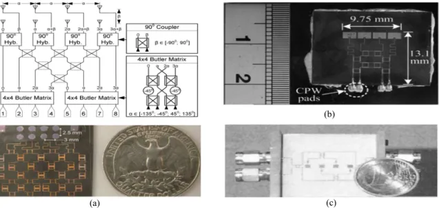
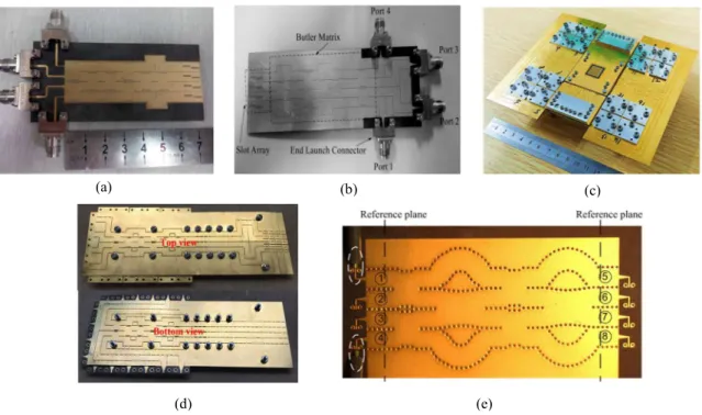
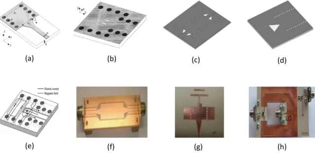
As mentioned previously, the BFNs could be considered as the heart of multi-beam antenna system due to its ability to direct the main beam of the antenna pattern towards different directions based on the signal created by itself. Since the early 1960s, a large number of well-known multiple-input-multiple-output (MIMO) ports solutions providing multi-beams by alternatively choosing the input excitation port have been proposed. These solutions can be categorized basically in two classes: matrices and lenses. We briefly consider here the most common ones, namely the Rotman Lens [7], the Blass [8]–[10], Nolen [11], [12], and Butler [13] matrices. The schematics of these techniques are illustrated in Figure 1-1.
Figure 1-1. (a) Rotman lens [14], (b) Blass matrix [10], (c) Nolen matrix [12] and (d) Butler matrix [15].
(a) (b)
(c) (d)
12
The Rotman lens was introduced by Rotman and Turner in the 1960s [7]. It is an RF beam-former with N inputs and M outputs. The RF signals from the input ports (beam ports) propagate through the lens cavity and are received by the output ports (antenna ports) before transmitting to the antenna array. The positions of the beam and antenna ports as well as the transmission line lengths are calculated by using the equations of optical path-length equality so that desired phase and amplitude distributions can be obtained [7]. An example of Rotman lens is reported in [14], consisting of a lens cavity, 14 antenna ports, 11 beam ports and 4 dummy ports. The lens cavity is used to focus the incident waves on the beam ports. The antenna ports are connected to antenna array, meanwhile the beam ports are for receiving the signal from the lens cavity. The dummy ports are terminated with loads for absorbing inter-cavity reflections. The delay lines are designed to compensate for the phases of the incoming waves from different angles [14]. Due to the multi-beam formation functionality, numerous researchers have lately found that Rotman lens is a promising candidate for real-time microwave or millimeter-wave imaging applications [16]. However, they are typically limited to far-field imaging, because their parallel multi-beam formation is based on the condition that the scattered waves arriving at the array are plane waves. In the near field, the non-plane waves scattered from a near-field target will spread across several beam ports of the Rotman lens. As a result, out-of-focus blurs appear in the near-field images. In addition, they usually suffer from low efficiency due to spillover losses and high coupling between adjacent ports, which make them less suitable for high power applications [16].
According to the feeding method, the matrix-based BFNs could be divided into two main categories: corporate and series feeds [17]. Whereas the Nolen matrix and the Blass matrix utilize the series feed method, the BM, on the other hand, is a corporate multi-beam feed. While BM is usually designed with an equal number of input (multi-beam) and output (antenna) ports (N×N), Blass and Nolen matrices can be designed with an unequal number of inputs and outputs (M×N). In the Blass matrix, the two sets of transmission lines referred to as row and columns of the matrix are interconnected at each crossover by a directional coupler. At each crossover, a small portion of the signal is coupled to each column, ultimately exciting the corresponding arbitrary number of radiating elements. The signal applied at any input port propagates along the corresponding feed line. Each line is terminated with a matched load to absorb the residual signal. By feeding each input port, a different phase distribution is produced along the array, hence providing a different radiated beam orientation, depending on the various electrical path [8]. The Nolen matrix can be seen as a modified Blass matrix in which the diagonal couplers are replaced by simple bent transmission lines. Accordingly, the termination loads at the end of each feeding line in a standard Blass matrix are suppressed, resulting in theoretically lossless operation [12].
However, the lack of symmetry between input and output ports makes these matrices more complicated to design as the path to the outputs. Besides, the efficiency of Blass matrix and Nolen matrix are quite low due to high losses associated with the structures. Moreover, the magnitude and phase shift mismatches at the antenna ports also make these matrices less attractive. Compared to the Blass matrix and Nolen matrix, the BM has received a great interest with a vast amount of research efforts, and has been used
13
in a variety of applications. This is mainly due to the advantages of BM as compared to the other counterparts such as perfect matching, isolation and equal power division that can be obtained at the same time [18], [19]. In addition, BM has larger bandwidth, structural simplicity and lower loss than the other Blass or Nolen matrices. That explains why BM was chosen as the targeted device to be investigated in TRICOT project. Its working principle is detailed in the next section.
1.3 Butler Matrix overview
1.3.1 Principle
BM is certainly the most extensively investigated beam-forming network developed to feed multi-beam antenna systems due to its outstanding properties. A typical (𝑁 × 𝑁) BM has 𝑁 input (signal) ports to which power is applied, and 𝑁 output (antenna) ports to which 𝑁 antenna elements are connected, where 𝑁 is a power of 2. RF power is fed to the antenna elements with a progressive phase difference between antenna elements so that the main beam of multi-beam antenna system can be in the desired direction. The progressive output phases are obtained thanks to an attachment of 3-dB, 90° couplers, crossovers and fixed phase shifters. The beam direction is controlled by switching the input power to the desired input port, via a single-pole N-through, SPNT or switch.
The principle of a common (4 × 4) BM leading to four different phase states and thus to four beam directions 𝜃 at the output port, is illustrated in Figure 1-2, where the antenna radiation patterns are in the xOy plane, x being the axis in which the antenna elements are placed. Practically, the antenna elements are spaced by 𝜆 /2 between each other, 𝜆 being the free-space wavelength. The beam direction 𝜃 corresponds to an input signal entering through port i. If port 1 is excited, the progressive output phase between consecutive antenna elements ∆𝜑 is equal to 45°, which orients the main beam at 𝜃 = +14.5°. If port 3 is excited, the progressive output phase ∆𝜑 is equal to −135° and the main beam is directed to 𝜃 = +48.6°. Due to symmetry around the yOz plane, when port 2 or 4 is fed, we have the same absolute value of the phase of output signal and the beam direction but sign is inverted (+ or -) [20].
Figure 1-2. Working principle of conventional 4x4 BM. −90° +90° Antenna Input signal Δ𝜑 0 𝜃2= −48.6° 𝜃4= −14.5° 𝜃1 = +14.5° 𝜃3 = +48.6° y x z O 3-dB Coupler
14
Over the last decades, a huge number of different topologies have been studied and developed not only to facilitate the design and fabrication of BM but also to improve the BM performance. Therefore, in the next sections, an overview of these techniques will be introduced as well as the state-of-the-art of BM in both RF and mm-wave designs.
1.3.2 State-of-the-art of BM design technique
The most important thing when designing a BM is the ability to obtain the compromise between complexity and performance. Thus, numerous design techniques for simplification and improvement of BMs have been investigated with different transmission lines topologies:
planar transmission lines: micro-strip line (MS-line) ([17], [18], [19], [20]–[26], [27]–[36], [37]–[42]), coplanar waveguide (CPW): [47], [48]. Some designed were also developed in CMOS technology: [49]–[54].
Substrate Integrated Waveguide (SIW) technology: [51], [52], [53], [54]–[60], [61]–[70], [71]–[76].
Actually, the MS-line technology is the most commonly used for BM design in both single-layered and multi-layered substrate, especially for RF and microwave applications. Indeed, multi-layered transmission line technologies can be applied to avoid using crossovers [21], [22], [33], [40]. The avoidance of crossovers was also investigated to broaden the bandwidth in [22] and [40] by using multi-section coupled-line directional couplers in micro-strip multi-layer technology for both 4×4 and 8×8 BMs, respectively. For similar purpose, multi-layered CPW technology was also implemented in a 4×4 BM [48]. Furthermore, some non-2 BMs, such as 3×3 BM [25], quasi 6×6 BM [26] and 4×6 BM [39] designed in MS technology were also studied and developed to enrich the options of beam numbers and thus, improve the configuration flexibility.
As we know, in order to have more directional beams for better transmission performance, higher-order BMs are required. However, the number of elementary blocks exponentially increases with the order of the BMs [48]. Therefore, many researchers have studied on miniaturization of the effective size of the structure as for example in [44], [45]. Particularly, if the BMs are implemented in silicon-based technology, the increase of elementary blocks leads to the increase of the design complexity and chip area. Thus, the circuit miniaturization becomes crucial for single-chip CMOS realization. Several works have been done to solve this issue by using the multi-layer bifilar transformer [49], the subsector technique [50], or lumped elements [52].
In parallel, SIW technology [81] have drawn a lot of attention over the two last decades thanks to the its attractive features such as high Q factor, high power capability, low-loss, reduced weight, and no susceptibility to electromagnetic interference or wide instantaneous bandwidth features. A large number of investigated devices such as filters, mixers, couplers, antenna has been developed, as for example in [82]–[88]. Thus, the use of SIW technology appears to be a good candidate for the implementation of Butler Matrix as well as the smart antenna systems when compared to micro-strip or planar waveguide technologies. Based on the system requirements, the structure of SIW BM can be formed by considering single-layered [58], [60], [61], [75], [76], [80], or multi-layered substrate, [57], [59], [62], [63], [65], [70], [72], [73], [78], [79]. One of the main advantages of
multi-15
layered substrate over the single-layered one is obviously the size reduction thanks to the decrease of the number of crossovers. Nevertheless, another important factor when dealing with SIW is the simplicity in the design. In fact, single-layered appears to be facilitate the design, and this is the reason why many authors preferred dealing with single-layered structures.
Next, the sub-section 1.3.3 will provide a detailed description of the BM design technique in both MS-line and SIW technology for RF applications meanwhile in 1.3.4, these two techniques will be presented for mm-wave applications.
1.3.3 Butler Matrix design overview for RF applications in
MS-line and SIW technology
1.3.3.1 MS-line technology
As discussed previously, the MS-line technology is the most commonly used for BM design, especially for RF and microwave applications. Indeed, numerous researches have been done by using this technology either in single-layered or multi-layered substrate. Therefore, in this section, a detailed state-of-the-art of MS-line-based BM in RF will be introduced.
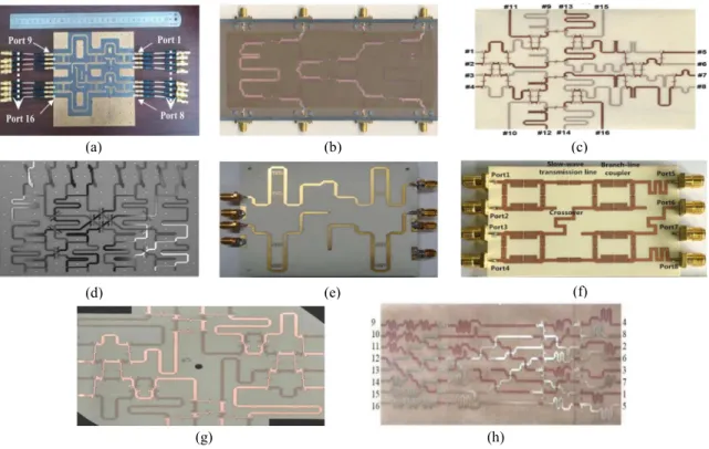
Figure 1-3. Butler matrixes based on single-layered microstrip in RF frequency band: (a) [31], (b) [32], (c) [35], (d) [37], (e) [44], (f) [45], (g) [46].
In Figure 1-3, several 4×4 MS single-layered BMs with different design methods are presented. Figure 1-3 (a) illustrates a BM using eight 3-branch-line couplers designed with lumped distributed elements to reduce the BM dimension. Multi-U-shaped coupled-line Schiffman phase shifters are also selected to achieve a good transmission and phase performance [31]. In Figure 1-3 (b), a miniaturized BM using 3-dB cross-slotted patch hybrid couplers is introduced[32] leading to an area reduction of 56% while maintaining a similar performance in comparison with that based on traditional patch hybrids. Another miniaturized BM is introduced in [35] (see Figure 1-3 (c)), the proposed BM is
(a) (b) (c)
(d) (e) (f)
16
implemented with couplers and crossovers considering stub-loaded transmission lines in order to obtain an area reduction of 55% as compared to the traditional one while maintaining the performance within the design frequency range.
A miniaturized BM based on a planar artificial transmission line is illustrated in Figure 1-3 (e) for application in ultra-high-frequency radio-frequency identification systems [44]. This planar artificial transmission line is based of micro-strip quasi-lumped elements and is capable of synthesizing micro-strip lines with various characteristic impedances and electrical lengths. By using this planar artificial transmission line, the circuit size of BM can be reduced 21% compared to the conventional one. Figure 1-3 (f) shows another size reduction technique for designing a BM by using a particular type of coupler which has swapped port characteristic wherein the locations of the isolation and coupled ports are switched, allowing obtaining a low 10% area reduction as compared to a conventional Butler matrix [45]. Finally, in Figure 1-3 (g), a compact BM is proposed using only one crossover. The second crossover and the output phase shifters are removed to avoid the interconnecting mismatch loss and imbalanced amplitude introduced by these phase shifters compared with the conventional one [46].
In Figure 1-3 (d), phase reconfigurable synthesized transmission lines are used to connect to the output of conventional BM to form an extended 4×4 BM [37]. This new design aims to provide a low-complexity solution to expand the beam controllability as well as spatial coverage of a conventional beam-switching system.
As an alternative to single-layered BMs, multi-layered MS technology can be used to design especially high-ordered MBs in order to reduce the structure complexity and circuit dimension, which extensively increases due to the escalation of elementary blocks. Several multi-layered MS based BM are presented in Figure 1-4.
A double-layer structure wide-band 8×8 BM is presented in [21], Figure 1-4 (a). The double layer structure is adopted to place components on the up and down layers without crossover, thus reducing the loss and size and is easy for producing. A three-branch line coupler is employed as a wideband bridge, and two-section stepped coupling microstrip Schiffman phase shifters are used to realize wideband phase shift. Figure 1-4 (b), a two-octave 4×4 BM was proposed in multi-layer microstrip asymmetric coupled- line technology [22]. To achieve two-octave frequency band in terms of amplitude and phase responses, multi-section coupled-line directional couplers and Schiffman C-sections are considered. A high performance three-section coupled-line 3-dB microstrip directional coupler is utilized as a basic element of the BM and compensated MS-line Schiffman C-sections are considered to provide appropriate differential phase characteristics. In [24], the use of coupled-line 3-dB/90° directional couplers and Schiffman phase shifters is also considered to ensure the broad-band amplitude and phase characteristics of the 8x8 BM (see Figure 1-4 (c)). In Figure 1-4 (d), a compact broad-band 8×8 Butler matrix integrated with tunable phase shifters is proposed to provide full beam switching/steering capability [28]. The strip-line tunable phase shifter is designed based on the asymmetric reflection-type configuration, where a Chebyshev matching network is utilized to convert the port impedance from 50 Ω to 25 Ω so that a phase tuning range in excess of 120° can be obtained. A 80% size reduction compared with a conventional BM was also achieved. In Figure 1-4 (e), a broad-band BM is proposed by combining a broad-band forward-wave
17
directional coupler and a broad-band middle network to obtain a large 47% relative bandwidth and a 67% size reduction as compared with the original size [34]. Meanwhile in Figure 1-4 (f) a slow-wave structure with high slow-wave factor is proposed. The structure is composed of meandered lines, low impedance transmission lines and interdigital structures and, for these reasons, is capable of reducing the circuit size significantly due to its good slow-wave property [36]. Another broad-band planar fully integrated 8×8 BM using coupled-line directional couplers is shown in [40], Figure 1-4 (g). A particular arrangement of the network allows the creation of an entirely planar design having two metallization layers and no interconnections between these layers. Four selected crossovers are realized as a tandem connection of two 3-dB/90 coupled-line directional couplers, which, together with reference transmission lines having appropriate electrical lengths, perform simultaneously crossovers of signal lines, and all needed broad-band constant value phase shifters. Moreover, two of the needed 3-dB/90 directional couplers are designed as tandem connections of two 8.34-dB directional couplers, acting as 3-dB/90 directional couplers having crossed outputs. Finally, a low-loss wideband flat-topped 8×8 BM is presented in Figure 1-4 (h). This BM is composed of double-side coupler loaded with open stubs and Schiffman phase shifter to get desired phase performance in a wide relative bandwidth of 60% [42].
Figure 1-4. Butler matrixes based on multi-layered microstrip in RF frequency band: (a) [21], (b) [22], (c) [24], (d) [28], (e) [34], (f) [36], (g) [40], (h) [42].
Table 1-1 compares state-of-the-art MS-line based BMs in both single-layered and multi-layered substrate for RF electronic applications. The reference, year/type, central frequency, size, BW, average transmission coefficient, maximum amplitude imbalance and phase imbalance at the central frequency, are listed. The BW is considered for an input impedance matching equal or better than 10 dB. Let us notice that ideally (without losses),
(a) (b) (c)
(d) (e) (f)
18
the average transmission coefficient should equal to -6 dB for a 4×4 BM, and -9dB for a 8×8 BM. It can be noticed from this state-of-art overview that one of the major claims is miniaturization of blocks, essentially couplers and phase shifters in multi-layered MS technology as crossovers may benefit from the multiple metallic layers opportunities. In the meantime this may be an issue for crossover isolation, as outlined in [89].
REF /Type Year Frequency (GHz) (mm×mm) Size (𝝀 × 𝝀) BW (%) (GHz) Avg. Trans.Coeff (dB) Max Amp.Imb (dB) Max Phase.Imb (°) Layers [44] (4x4) 2007 0.915 (0.49x0.54) 99x108 (0.89-0.99) 10.7 -8.6 ±1.1 ±7.5 single [45] 2010 (4x4) 1 70x70 (0.35x0.35) NA -8.3 ±0.9 ±8 single [28] (8x8) 2010 2.2 (2.16x1.35) 160x100 (1.6-2.8) 56 -10.1 ±2.2 ±20.7 multi [22] 2010 (4x4) 3 NA 113 (1.12-4.5) -7.1 ±0.9 ±10 multi [31] (4x4) 2011 5 (2.65x2.92) 86.5x95.3 (4.5-5.5) 20 -7.5 ±1.5 ±10 single [40] (8x8) 2011 3 (2.39x1.83) 130x100 (2.5-3.5) 33 -7.2 ±0.45 ±7.5 multi [21] 2013 (8x8) 5 150x150 (4x4) (4.7-5.2) 10 -13.2 ±1.5 ±12 multi [32] (4x4) 2013 2.4 (1.3x1.15) 85x75 (2.2-2.5) 14 -7.3 ±0.7 ±5 single [34] (4x4) 2013 2.5 81.65x71.56 (1.17x1.02) (1.96-3.15) 47 -7.1 ±1 ±6 multi [33] 2014 (8x8) 4.3 150x150 (4x4) 23.2 (3.7-4.7) -14.2 ±2 ±15 multi [46] (4x4) 2014 6 NA (5.4-6.6) 20.1 -7.24 ±0.4 ±0.9 single [35] (4x4) 2014 2.4 NA (2.2-2.6) 16.7 -8.2 ±1.5 ±2.1 single [24] (8x8) 2016 3 (1.4x1.2) 170x145 (2-4) 33 -10.1 ±0.5 ±10 multi [36] (4x4) 2017 0.97 (0.42x0.22) 76x39 (0.92-1.06) 14.4 -7.31 ±1.2 ±6.85 multi [37] 2018 (4x4) 2.4 (2.07x2.11) 137.6x140 (2.2-2.6) 16.7 -7.7 ±1.2 ±9.3 single [42] (4x4) 2020 9 NA 60(5-12) -9.1 ±1.5 ±8 multi
Table 1-1. Summary of State-of-the-art MS-based BM in RF frequency band.
1.3.3.2 SIW technology
Contrary to the large amount of research work for MS-line based BM in RF applications, a limited number of publications concerning the design of SIW-based BM has been found in literature. Figure 1-5 shows several kinds of BM based on SIW technology for RF applications.
In Figure 1-5 (a), a 4×4 single-layered BM designed in Ku-band is presented [76]. Thanks to improved cross-couplers, a 24% relative frequency bandwidth is obtained. Figure 1-5 (b) illustrates a multi-layered SIW BM beam-forming network designed for 24-GHz automotive radar systems [79]. In this structure, a SIW H-plane coupler is optimized
19
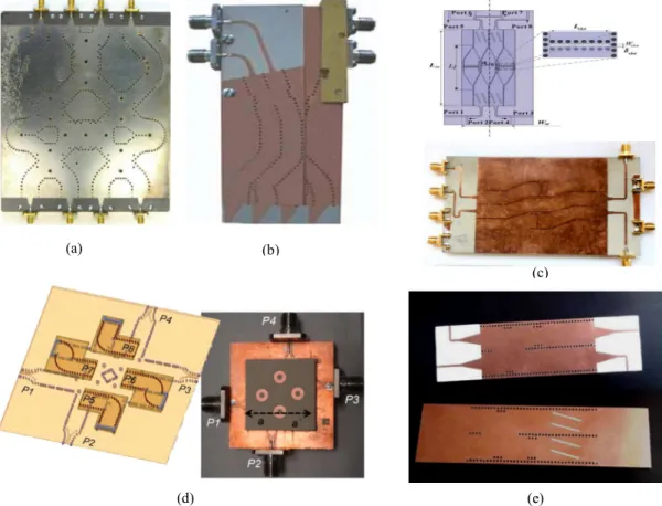
with an H-plane slit to provide the required phase shift. A class of SIW E-plane 3-dB couplers in doubled layer substrate is considered as the fundamental building blocks to avoid crossovers. Meanwhile, a particular technique to design a compact wideband 4×4 BM for Ku-band applications is presented in [78], see Figure 1-5 (c). In this article, a two-layer SIW BM is designed through a two-fold enhancement approach leading to a significant size reduction of about 50% with respect to the traditional one. In Figure 1-5 (d), a BM-fed two-dimensional scan linearly polarized 2×2 microstrip ring antenna array which is designed in low-cost SIW technology for Ka-band applications is introduced [57]. The highly efficient, compact and passive BM is designed with SIW cruciform couplers and its special topology is well adapted for feeding antenna arrays. Finally, in Figure 1-5 (e), a broad-band 4×4 SIW multi-layered BM operated at central frequency of 9.5 GHz is presented. The proposed Butler matrix consists of two 90° couplers and a broad-band phase shifter that allows to obtain a broad-band operated frequency range and achieve a compact BM thanks to the absence of crossovers [59].
Figure 1-5. Butler matrixes based on SIW technology in RF frequency band: (a) [76], (b) [79], (c) [78], (d) [57], (e) [59].
The performance of these BMs is presented in Table 1-2. Let us notice that due to large lateral dimensions of the SIWs, only frequencies above about 10 GHz are addressed in this technology.
(a) (b)
(c)
20
REF /Type Year Frequency (GHz) (mm×mm) Size (𝝀 × 𝝀) BW (%) (GHz) Avg. Trans.Coeff (dB) Max Amp.Imb (dB) Max Phase.Imb (°) Layers [76] (4x4) 2010 12.5 144x146 (6x6.08) (11-14) 24 -7.5 ±1 ±15 single [78] (4x4) 2011 12.5 36.25x83.18 (1.51x3.46) (11-14) 24 -6.7 ±0.6 ±7 multi [79]* (4x4) 2012 24 (4.08x2.24) 51x28 (22-26) 16.67 -6.35 ±0.11 ±5 multi [57]* (4x4) 2014 26.5 NA (25-28) 10.71 -7.3 ±0.75 ±12 multi [59] (4x4) 2015 9.5 (1.74x1.07) 55x34 (7.5-11.5) 42.1 -6.2 ±0.6 ±5 multi
Table 1-2. Summary of the State-of-the-art SIW-based BM in RF frequency band. (*) the results of the BM are simulated but the entire antenna system was fabricated and measured
1.3.4 Butler Matrix design overview for mm-wave applications in
MS-line and SIW technology
1.3.4.1 MS-line technology
In contrast to the huge number of MS-line-based BMs in RF band, only a few works have been done to design the MS-line-based BM for mm-wave applications. It is mainly due to the design and fabrication tolerances in high frequency PCB technology as well as the radiation losses, which increase at higher frequency. However, because of its low cost, the use of microstrip technology for BM realization in mm-wave stays interesting, especially for mm-wave on-chip radio. Three examples of 4×4 BM designed for mm-wave applications are presented in Figure 1-6.
Figure 1-6 (a) shows a 60-GHz two-dimensionally scanning array employing wide band planar switched beam network which is composed of two 4×4 MS-line based BM and four hybrid couplers designed in low cost PCB technology [27]. The network has eight I/O ports, each producing a different beam. The first four ports span one BM and the last four ports span the other. The selection of the Butler matrix (left or right) determines the E-plane scan angle, and the selection of port within the matrix determines the H-plane scan angle. The measured results show that this network causes approximately 2 dB of loss in the band of interest and the peak realized gain of the array is achieved at 12.3 dBi. Another 60-GHz switched-beam patch antenna array with 4×4 BM network is also illustrated in Figure 1-6 (b) [30]. By using this network, a return loss greater than 9.6 dB can be obtained over the frequency range of 59.7-65 GHz, meanwhile the maximum insertion loss is found to be around 1.7 dB. Finally, in Figure 1-6 (c), a 4×4 BM with millimeter microstrip is designed at around 40 GHz without any crossing on single-layered substrate. However, the parasitic radiations of the feeding network (which is the Butler matrix) slightly affect the antenna radiating patterns by an increase of the side-lobes levels in the H-plane and thus narrower beams [29].
21
Figure 1-6. Butler matrixes based on microstrip in mm-wave frequency band: (a) [27], (b) [30], (c) [29].
1.3.4.2 SIW technology
For mm-wave applications, MS-line technology has not attracted many interests to design the BM, whereas the use of SIW technology is much more preferred for this issue. It is mainly due to its characteristics to reduce insertion losses compared to other planar technologies while maintaining most advantages of such technology such as high Q-factor, high power capability, high integration, manufacturing simplicity, low weight, etc. Thus, in this section, a detailed description of SIW-based BMs designed for mm-wave application is presented. Several kinds of mm-wave SIW-based BMs are illustrated in
Figure 1-7.
In Figure 1-7 (a), a single-layered SIW multi-beam slot array operating at about 30 GHz for future 5G mobile terminal application is presented [60]. The multi-beam forming network is realized with a Butler matrix that is composed of hybrid couplers, crossovers, and phase shifters (135° and 0°). By using this BM, the transmission coefficients of port 1 and port 2 (as input ports) could be found respectively at -7.0±0.8 dB and -7.0±2.8 dB while the maximum phase error is only approximately 6°. Another single-layered SIW multi-beam slot array operating from 28 to 32 GHz also used for 5G applications is illustrated in [61], Figure 1-7 (b). This particular BM is designed by using a modified hybrid coupler followed by a -45° compensating phase shifter. The modified hybrid coupler is capable of outputting 45°/135° phase differences and exhibits excellent performance with wideband and flat phase balance, 135° ± 1.8° and 45° ± 1.8° in the completely operating band. This enables phase dispersions of the designed Butler matrix with peak-to-peak error of 13°, for both port 1 or port 2 excitations; coupling to the output ports is well equalized at −6.3 dB with 1.2 dB dispersion across the entire operating bandwidth of interest from 28 GHz to 32 GHz.
(a)
(b)
22
Figure 1-7. Butler Matrixes based on SIW in mm-wave frequency band: (a) [60], (b) [61], (c) [72], (d) [73], (e) [75].
Figure 1-7 (c) presents a millimeter-wave 2-D multi-beam aperture-coupled magneto-electric dipole antenna array operating at 60-GHz band [72]. This antenna array is fed by two sets of 4x4 SIW BM arranged in orthogonal directions. The simulated S-parameters show that the impedance bandwidth is wider than 22.6% for reflection coefficients of less than −10 dB from 54.2 to 68 GHz. Besides, the insertion loss of the Butler matrix is less than 1.5 dB, the difference in power between different output ports is less than 1.4 dB, the isolation between any two output ports is larger than 14 dB and finally, the maximum phase error is less than ±9° over the operating band from 56 to 65 GHz. Another millimeter-wave 2-D beam-scanning multi-beam array antenna fed by multi-layered SIW BFN is illustrated in Figure 1-7 (d) [73]. The BFN is formed by connecting two stacks of sub-BFNs, the E-plane sub-BFN and the H-plane sub-BFN. The H-plane sub-BFN is realized by a traditional H-plane 4×4 BM. The key point of this design is to propose an E-plane 4x4 BM which realizes a planar E-plane sub-BFN. These two sets of sub-BFNs can joint directly without resorting to any connectors or connecting networks to form such a compact 16-way BFN with a reduced area. For the E-plane BM, from 28 to 32 GHz, the return loss and isolation coefficients between distinguished output ports are better than 18 dB. At the center frequency (30 GHz), the phase and amplitude errors are lower than ±3° and ±0.8 dB, respectively. The biggest errors are observed at 28 GHz with ±18° for phase error and ±2 dB for amplitude error. The average insertion loss of the total E-plane BM is about 0.97 dB. Meanwhile for the H-plane BM, from 28 to 32 GHz, the phase peak-to-peak errors are less than ±15°. The average insertion loss of the H-plane BM is about 0.47 dB. Finally, a 60-GHz SIW BM which is designed and fabricated by a standard single-layer PCB process is illustrated in Figure 1-7 (e) [75]. As the measured results of the proposed BM show, for the operating bandwidth from 58 to 62 GHz, the reflections and isolations are lower than -13.5 dB and the insertion losses are below 2.5 dB meanwhile the phase peak-to-peak errors are less than ±17°.
(a) (b) (c)
23
In order to have an overview of the development of mm-wave SIW-based BMs, a performance summary of the state-of-the-art of these BMs during the last decade will be introduced in Table 1-3.
REF /Type Year (GHz) Freq.
Size (mm×mm) (𝝀 × 𝝀) BW (%) (GHz) Avg. Trans.Coeff (dB) Max Amp.Imb (dB) Max Phase.Imb (°) Layers [75] 2010 (4x4) 60 (5.42x3.56) 27.1x17.8 (48-67) 31.7 -8.2 ±1.5 ±17 single [80]* 2012 (4x4) 77 (8.09x7.31) 31.5x28.5 (72-81.5) 12.3 -6.7 ±0.3 ±4 single [58]* 2015 (4x4) 60 14.98x17.75 (3x3.55) (57-64) 11.67 -7 ±1.5 ±14 single [60]* 2016 (4x4) 30 (6.19x2.74) 61.9x27.4 (28-32) 13.3 -6.8 ±1 ±10 single [61]* 2016 (4x4) 30 (11.03x4.25)** 110x42.5 (28-32) 13.3 -6.75 ±0.7 ±7 single [63]* 2017 (4x8) 38 NA 10.5 (36-40) -10.8 ±0.8 ±5 multi [65]* 2017 (8x8) 29.5 101.7x40.68 (10.4x4.6) (28-31) 10.17 -11 NA ±15 multi [62]* 2017 (4x4) 60 NA (50-70) 33.3 -8.2 ±1 ±5 multi [70]* 2017 (4x4) 94 NA (93-95) 2.13 -7.2 ±0.3 ±5 multi [72]* 2017 (4x4) 60 150x150 (30x30) (54.68) 23.33 -7.5 ±1.4 ±9 multi [73]* 2018 (4x4) 30 (16.5x4.5) 165x45 (28-32) 14.29 -7 ±2 ±18 multi
Table 1-3. Summary of the State-of-the-art SIW-based BM in mm-wave frequency band. (*) the results of the BM are simulated but the entire antenna system was fabricated and measured (**) area including access lines and antennas
1.3.5 Pros and Cons
As mentioned previously, over the two last decades, the BM have attracted a lot of attention compared to the others beam-forming networks due to its outstanding characteristics such as perfect matching, isolation and equal power division that can be obtained at the same time. In addition, BM has realizable large bandwidth, its structural simplicity and very low power consumption. By combining with SIW technology, the SIW-based BMs step-by-step have become an unbeatable candidate for designing smart antenna system that is an essential component for future communication networks.
However, some drawbacks are still existing that require to be further studied and dealt with. The first problem is the structure dimension. Even when the multi-layered substrate was used to avoid using the crossovers, the total area of investigated SIW BMs remains large. Therefore, a necessary method is required to miniaturize theses SIW-based BMs. Thus, in this thesis, a slow-wave effect will be considered as a solution for the miniaturization of SIW-based BMs, especially at 28 GHz in PCB technology. This method will be detailed in Chapter 4 and Chapter 5.
Another drawback needs to be considered when designing a SIW-based BM: that is the sensitivity of elementary blocks such as couplers, crossovers and phase shifters,
24
which has a high impact on the BM performance, especially the sensitivity in transmission path isolation of the crossover. Indeed, as indicated in [89], when the crossover transmission path isolation (𝑆 ) varies from 35 dB down to 15 dB, the output amplitude imbalance goes from 0.33 dB to 3.6 dB and the output phase imbalance goes from 1.5° to about 18°. Therefore, a good transmission path isolation (at least better than 25 dB) needs to be achieved when designing the crossover in order to maintain a good BM performance.
1.4 Low-loss and compact Substrate Integrated Waveguides
In this thesis, elementary blocks of BM will be designed in both RF and mm-wave frequency band. Thanks to its attractive features such as high Q factor, high power capability, low-loss, reduced weight that have been demonstrated in literature, SIW technology will be considered as a selection for guided transmission topology for our circuits in RF frequency band. Nevertheless, SIW is a substrate-based structure and hence it still suffers from dielectric losses increasing at high frequency. Therefore, in this thesis, three topologies of SIW will be studied.
First, in Chapter 3, an Air-Filled SIW (AF-SIW) will be studied for mm-wave applications in a particular interposer technology based on Carbon-Nanotubes (CNT). Then, in order to obtain a compact Air-Filled SIW, two topologies of slow-wave SIW (SW-SIW) will be studied. Based on CNT technology, an AF-SW-SIW will be designed in Chapter 4 and finally, a proof-of-concept will be proposed in PCB technology at 28 GHz for 5G applications and will be presented in Chapter 5. In that case, a Partially Air-Filled SWave SIW (PAF-SW-SIW) will be considered. Hence, a compromise between low-loss and compactness will be addressed by using respectively, air-filled technology and slow-wave effect. Finally, in order to evaluate the proof-of-concept performance, the two topologies of AF-SW-SIW and PAF-SW-SIW will be compared.
Hence, before presenting the considered waveguide topologies (in Chapter 3, Chapter 4, and Chapter 5), a general description of SIWs, miniaturization techniques and air-filled structures will be introduced in this section.
1.4.1 SIW structure
Whereas the classical metallic rectangular waveguide (RWG) is an extremely low-loss structure, it suffers of heavy weight, low integration capability and high cost of fabrication. On the other hand, the planar transmission lines although have lower Q-factors, they possess lightweight structure and especially a cheap fabrication process. Therefore, the Substrate Integrated Waveguide (SIW), which possesses the advantages of both aforementioned technologies, has been extensively studied in the past 20 years and has become an outstanding candidate for RF systems. Generally, SIW is a rectangular waveguide-based structure realized in low-profile technology such as printed circuit board (PCB) technology with two metallized layers [81]. The upper and lower substrate metallization are used as the top and bottom walls of the waveguide structure whereas the lateral walls are synthesized in the form of two rows of conducting metallic vias embedded in the dielectric substrate (see Figure 1-8). As for RWG, the main geometrical parameters of a SIW are its width 𝑊 and height ℎ. Two other parameters are introduced, the via-holes diameter 𝑑 and their longitudinal spacing 𝑠.
25
Figure 1-8. SIW geometry [90].
Because the electric side walls of SIW structure are constructed by two parallel via arrays, the associated longitudinal currents cannot travel along the lateral walls, thus only TE mode can be propagated inside SIW with the vertical electric current density on the side walls [91]. The cut-off frequency corresponding to 𝑇𝐸 modes can be described via the equivalent RWG width 𝑊 , as shown in (1-1), where 𝑊 corresponds to the width of a classical RWG having the same electrical characteristics as the SIW structure with its real width 𝑊, 𝜀 being the dielectric constant of the substrate [81].
𝑓 = ×
× ×√ (1-1)
The first mode also called fundamental mode is the 𝑇𝐸 mode is calculated in (1-2)
𝑓 =
× ×√ (1-2)
The second mode called 𝑇𝐸 appears at 2𝑓 . Hence, the first-mode bandwidth is limited by 𝑓 and 2𝑓 . In a practical manner, the operating frequency band of the 𝑇𝐸 mode is then considered between 1.2𝑓 and 1.8𝑓 [92].
Over the last decade, many publications aimed to study, analyze and develop the design rules for SIW circuit design. These design rules are based on three different principles [90] summarized as follow:
Minimize the leakage between the via holes
Avoid the presence of bandgaps within the operating frequency band
Limit the mechanical impact of drilling by avoiding very high densities of via-holes
The fundamental design rules for the proper operation of SIW were investigated in [93] and were more detailed in [81]. First, the condition 𝑠 > 𝑑 should be followed for obvious practical reasons. Then by combining all consideration, the two following rules were given:
0.05 < < 0.25 (1-3) 𝑠 ≤ 2𝑑 (1-4) where 𝜆 is the cut-off wavelength related to the cut-off frequency 𝑓 by 𝑓 = 1/(𝜆 √𝜖𝜇)
The equation (1-3) is related to bandgap consideration, while the equation (1-4) reflects an arbitrary mechanical consideration that aims at avoiding unnecessary drilling.
26
Moreover, the equation (1-4) presents a sufficient condition for negligible leakage losses. By using the dispersion properties extracted from the Boundary Integral-Resonant Mode Expansion (BI-RME) method combined with the Floquet’s theorem [94], an empirical equation was extracted to link the effective width 𝑊 of a conventional RWG and the real width 𝑊 of SIW structure which has the same characteristics. This equation is shown in (1-5):
𝑊 = 𝑊 −
. (1-5)
An accurate formula of the equivalent width 𝑊 is introduced in [91] by studying the leakage characteristics of SIW based on a numerical multimode calibration procedure. This new equation takes the dispersion effect generated by the ratio 𝑑/𝑊 into account. Thus, the SIW propagation constant can match this from a RWG as depicted in [91]. This equation is given in (1-6):
𝑊 = 𝑊 − 1.08 + 0.1 (1-6) After having some physical parameters of the SIW waveguide, full-mode analysis can be carried out by electromagnetic simulation software.
1.4.2 SIW miniaturization techniques
Thanks to its outstanding performance as compared to planar transmission lines, SIW structures have still drawn a lot of attention for the research activities in recent years. As mentioned previously, one intrinsic and major drawback of the SIW is its huge lateral dimension as compared to classical planar transmission lines (e.g. microstrip, CPW). Therefore, the dimension miniaturization became one of the critical issues of performance improvement of SIW-based structures. Thus, in this section, some techniques to reduce the SIW-based structure dimension are presented.
As illustrated in Figure 1-9, the ridge SIW is known as a first solution to reduce the large dimension of a well-known classical metallic waveguide. The structure of the ridge waveguide is quite similar to the rectangular waveguide with one or two ridges inserted in the center of the waveguide. This principle was first published in 1947 by S. B. Cohn [95]. In this publication, it was found that a lower cut-off frequency can be achieved into the ridge waveguide at the same dimension of the hollow metallic waveguide.
Figure 1-9. (a) Single and (b) double ridge rectangular waveguide cross-section [95].
Thanks to the possibility of multi-layer configuration in PCB technology, the ridge concept has been adapted in 2007 for broad-band transitions from microstrip to SIW [96], as presented in Figure 1-10 (a). With the development of SIW technology, the ridge SIW could be easily implemented into a dielectric substrate by using the conductive vias array
27
to form the lateral walls and the blind vias for ridge support [97], as depicted in Figure 1-10 (b). In this article, the authors demonstrated that a metal strip connecting all blind vias could be used to remove the bandgap effect related to the periodicity and improve the bandwidth to three times that of the usual SIW.
Figure 1-10. (a) Transition from microstrip to SIW based on Ridge SIW [96] and (b) Ridge waveguide with the connection of the blind via holes for band-gap removal [97].
It was also demonstrated that an interesting 37% expansion of mono-mode bandwidth [98], as well as lateral miniaturization up to 40% [99] could be achieved. Recently, a novel ridge-SIW-based humidity sensor combined with quarter-mode technique was studied and developed in [100], where the occupied surface is only 20% of the whole surface of the classical SIW sensor.
The second technique to reduce the SIW-based circuits size is so-called “folded SIW”. It also relies on a multi-layer configuration. The idea is to bend the waveguide in order to reduce its lateral dimension. It was first introduced by W. L. Barrow in 1941 [101], see Figure 1-11 (a). By folding the wave path inside the waveguide, a very low cut-off frequency can be obtained for the same width of a standard waveguide. In this waveguide, the miniaturization is directly related to the number of bends.
The folded waveguide was first adapted in SIW technology in 2004 [102], and later applied to the design of several passive components. Depending on the way they are bent, the transversely folded SIW can be classified into two main categories: “C-“ or “T-shape”, respectively presented in Figure 1-11 (b) and (c). From the technology point-of-view, the T-shape configuration has the advantage of presenting a vertical symmetric electric field distribution over the C-shape, facilitating the excitation. However, both structures must be realized in a multi-layered substrate, thus increasing the fabrication cost. A “L-shape” was also introduced in [103] for the feeding of folded tapered slot antenna.
Figure 1-11. (a) Folded rectangular waveguide as introduced by W. L. Barrow [101], (b) Folded SIW in C shape and (c) in T shape [104].
After the first publication in 2004 [105], the C-shape configuration has attracted much more attention as compared to the T-shape geometry. It is mainly because the
“C-(a) (b)