UNIVERSITÉ DE MONTRÉAL
HIGH DATA-RATE, BATTERY-FREE, ACTIVE MILLIMETER-WAVE IDENTIFICATION TECHNOLOGIES FOR FUTURE INTEGRATED SENSING, TRACKING, AND
COMMUNICATING SYSTEMS-ON-CHIP
PASCAL BURASA
DÉPARTEMENT DE GÉNIE ÉLECTRIQUE ÉCOLE POLYTECHNIQUE DE MONTRÉAL
THÈSE PRÉSENTÉE EN VUE DE L’OBTENTION DU DIPLÔME DE PHILOSOPHIAE DOCTOR
(GÉNIE ÉLECTRIQUE) DÉCEMBRE 2016
UNIVERSITÉ DE MONTRÉAL
ÉCOLE POLYTECHNIQUE DE MONTRÉAL
Cette thèse intitulée:
HIGH DATA-RATE, BATTERY-FREE, ACTIVE MILLIMETER-WAVE IDENTIFICATION TECHNOLOGIES FOR FUTURE INTEGRATED SENSING, TRACKING, AND
COMMUNICATING SYSTEMS-ON-CHIP
présentée par : BURASA Pascal
en vue de l’obtention du diplôme de : Philosophiae Doctor a été dûment acceptée par le jury d’examen constitué de :
M. LAURIN Jean-Jacques, Ph.D., président
M. WU Ke, Ph.D., membre et directeur de recherche
M. CONSTANTIN Nicolas, Ph.D., membre et codirecteur de recherche M. FRIGON Jean-François, Ph.D., membre
DEDICATION
To my parents, my sisters, my brothers, my aunts, my uncles, my cousins, and all my loved ones “It is much more humbling to imagine this little step shining your faces and giving you a smile”
ACKNOWLEDGEMENTS
First and foremost, I would like to take this opportunity to express my utmost gratitude to my supervisor, Professor Ke Wu, for having given me the opportunity to join his research team. I am deeply indebted to him for his inspiring guidance, patience, and support throughout my Ph.D. studies.
I would like to extend my thanks to my thesis co-supervisor Professor Nicolas Constantin, for his help and encouragement during the long years that I have spent working on my dissertation.
I would also like to thank the members of my thesis jury, Professor Jean-Jacques Laurin, Professor Jean-François Frigon, and Professor Frédéric Nabki, for having accepted to examine this work, for the time and effort they have put forth, and for their valuable comments.
A special thanks goes to Professor Tarek Djerafi, for his willingness to help and for the contribution he made on this work.
To my Poly-Grames Research Center colleagues at the Ecole Polytechnique de Montreal, the list will be too long, thank you for creating a pleasant and stimulating environment for research.
I would like to thank all technical staffs of the Poly-Grames Research Center, Mr. Jules Gauthier, Mr. Jean-Sebastien Décarie, Mr. Traian Antonescu, Mr. Steve Dubé, and Mr. Maxime Thibault, for their professional assistance in the fabrication and the measurements. Thank you Mme. Rachel Lortie, our Poly-Grames Research Center secretary, for your enthusiastic service.
The technical support, design tools, and chip fabrication from CMC Microsystems, Kingston, ON, Canada, is gratefully acknowledged.
RÉSUMÉ
Pour de nombreuses applications allant de la sécurité, le contrôle d'accès, la surveillance et la gestion de la chaîne d'approvisionnement aux applications biomédicales et d'imagerie parmi tant d'autres, l'identification par radiofréquence (RFID) a énormément influencé notre quotidien. Jusqu'à présent, cette technologie émergente a été la plupart du temps conçue et développé dans les basses fréquences (en dessous de 3 GHz). D’une part, pour des applications où de courte distances (quelques centimètres) et à faible taux de communications de données sont suffisantes (même préférables dans certains cas), la technologie RFID à couplage inductif qui fonctionne à basse fréquences (LF) ou à haute fréquences (HF) fonctionne très bien et elle est largement utilisée dans de nombreuses applications commerciales. D'autre part, afin d’augmenter la distance de communication (quelques mètres), le débit de données de communication, et ainsi minimiser la taille du tag, la technologie RFID fonctionnant dans la bande d’ultra-haute fréquence (UHF) et aux fréquences micro-ondes (par exemple, 2.4 GHz) a récemment attiré beaucoup d'attention dans le milieu de la recherche et le développement. Cependant, dans ces bandes de fréquences, une bande passante disponible restreinte avec la taille du tag assez large (principalement dominée par la taille d'antenne et de la batterie dans le cas d'un tag actif) sont les principaux facteurs qui ont toujours limité l'évolution de la technologie RFID actuelle. En effet, propulser la technologie RFID dans la bande de fréquences à ondes millimétriques briserait les barrières actuelles de la technologie RFID.
La technologie d’identification aux fréquences à ondes millimétriques (MMID) offre plus de bande passante, et permet également la miniaturisation de la taille du tag, car à ces bandes de fréquences, la longueur d’onde est de l’ordre de quelques millimètres, une taille comparable à la taille d’un circuit intégré. L'antenne peut donc être soit intégré sur la même puce (antenne sur puce) ou soit encapsulé dans le même boitier que le circuit intégré. En dotant le tag la capacité de récolter sans fil son énergie à partir d'un signal aux fréquences à ondes millimétriques provenant du lecteur, lui fournissant ainsi l'autonomie énergétique (ainsi éliminant la nécessité d'une batterie et en même temps permettant la miniaturisation du tag), il devient alors possible d'intégrer entièrement tout le tag MMID sur une seule puce y compris les antennes, ce qui aboutira à la mise au point d’une nouvelle technologie miniature (µRFID) fonctionnant à la bande de fréquences à ondes millimétriques. En outre, le concept d’identification aux fréquences à ondes millimétriques est
compatible avec des applications à venir de la technologie aux fréquences à ondes millimétriques dans le domaine de la communication sans fil tels que l’internet des objets "Internet of Things", la technologie 5G, etc.
Dans cette thèse, nous présentons et démontrons le concept d’identification aux fréquences à ondes millimétriques pour un système actif, mais sans batterie, entièrement intégré sur en utilisant le procédé de fabrication de circuits intégrés moins chère, standard, et commercial CMOS. La technologie MMID proposée dans cette thèse, représente la prochaine génération de la technologie RFID miniaturisée (μRFID) opérant à des fréquences à ondes millimétriques. Les notions clés de la technologie RFID, le redresseur de l'énergie sans fil, les motivations, les contributions, et ainsi l'organisation de la thèse sont abordées aux chapitres 1 et 2. Le chapitre 3 présente l'étude et la démonstration expérimentale qui prouve que l'énergie RF peut être récoltée et efficacement convertie en énergie CC utilisable même aux fréquences à ondes millimétriques. Dans le chapitre 4, le concept d’un mélangeur auto-oscillant, approprié aux circuits intégrés à ultra-faible consommation de puissance (émetteurs-récepteurs auto-alimentés) est proposé et analytiquement et expérimentalement démontré aux fréquences à ondes millimétriques. Le chapitre 5 démontre un tag MMID miniature intégré sur un seul chip y compris les antennes intégrées dans le boîtier. Le tag est capable de recevoir sans fil (aux fréquences à ondes millimétriques) son énergie grâce au convertisseur intégré sur puce, d’alimenter son émetteur-récepteur intégré aussi sur puce, et d’échanger ses données avec le lecteur à un haut débit de communication. Le chapitre 6 aborde le concept d'antenne sur puce, un élément clé dans l’aboutissement et la mise en œuvre d’un tag MMID entièrement intégré sur puce. Une antenne à fente "slot antenna" double fréquences intégrée sur puce est proposée. Les résultats obtenus démontrent expérimentalement qu’une efficacité et un gain largement suffisants pour les applications MMID sont réalisables. Le chapitre 7 présente les applications potentielles du concept MMID proposé dans cette thèse. Enfin, une conclusion et les travaux futurs sont présentés au chapitre 8.
ABSTRACT
For countless applications ranging from security, access control, monitoring, and supply chain management to biomedical and imaging applications among many others, radio frequency identification (RFID) technology has tremendously impacted our daily life. So far, this ever-needed and emerging technology has been mostly designed and developed at low RF frequencies (below 3-GHz). For many practical applications where short-range (few centimeters) and low data-rate communications are sufficient and in some cases even preferable, inductively coupled RFID systems that operate over either low-frequency (LF) or high-frequency (HF) bands have performed quite well and have been widely used for practical and commercial applications. On the other hand, in the quest for a longer communication range (few meters), relatively high data-rate and smaller antenna size RFID systems operating over ultra-high frequency (UHF) and microwave frequency bands (e.g., 2.4-GHz) have recently attracted much attention in the research and development community. However, over these RF bands, a restricted available bandwidth together with an undesired tag size (mainly dominated by its off-chip antenna size and battery in the case of active tag) are the main factors that have been limiting the evolution of today’s RFID technology. Indeed, propelling RFID technology into millimeter-wave frequencies opens up new applications that cannot be made possible today.
Millimeter-wave identification (MMID) technology is set out to exploit significantly larger bandwidth and smaller antenna size. Over these frequency bands, an effective wavelength is in the order of a few millimeters, hence close to a typical semiconductor (CMOS) die size. The antenna, therefore, may either be integrated on the same chip (antenna-on-chip – AoC) or embedded in the related package (antenna-in-package – AiP). In addition, by equipping the tag with the capability to wirelessly harvest its energy from an incoming millimeter-wave signal, thereby providing energy autonomy without the need of a battery and at the same time allowing miniaturization, it becomes possible to integrate the entire MMID tag circuitry on a single chip. Furthermore, the timely MMID concept is fully compatible with upcoming and future applications of millimeter-wave technology in wireless communications which are being discussed and developed worldwide in research and development communities, such as the internet of things (IoT), 5G, autonomous mobility, µSmart sensors, automotive RADAR technologies, etc.
This thesis introduces and demonstrates a high data-rate, battery-free, yet active MMID concept, fully implemented on a single CMOS-die (an all-in-one solution using a commercial standard CMOS process). The proposed MMID system represents the next generation of µRFID technology that operates at mm-wave frequencies. Key notions of RFID technology and wireless power harvesting, the motivation, the contributions and the thesis organization are discussed in Chapter 1 and 2. Chapter 3 presents the study and experimental demonstration that RF energy can still be harvested and efficiently converted into DC power even at mm-wave frequencies. In Chapter 4, a zero-IF self-oscillating mixer concept, applied as an ultra-low-power transceiver suitable for self-powered devices, is proposed and demonstrated at mm-wave frequencies. In Chapter 5, the antenna-in-package concept is exploited, and it demonstrates the realization of a miniature high data-rate MMID tag on a single-chip. The MMID tag harvests its energy from the reader (i.e. it is entirely supplied by the on-chip mm-wave/DC energy converter) and exchanges data at a high bit-rate for both communication links. Chapter 6 addresses the antenna on-chip concept, a key circuit block that renders possible the full implementation of the MMID tag (i.e. including the antenna) on a single CMOS-die. An on-chip, dual-frequency rectangular slot antenna with a DRA loading is proposed and studied, and it is experimentally demonstrated that sufficient radiation efficiency and antenna gain for both bands are achievable. Chapter 7 discusses potential applications of the proposed MMID concept in this thesis. Finally, a conclusion and future works are presented in Chapter 8.
TABLE OF CONTENTS
DEDICATION ... III ACKNOWLEDGEMENTS ... IV RÉSUMÉ ... V ABSTRACT ...VII TABLE OF CONTENTS ... IX LIST OF TABLES ...XII LIST OF FIGURES ... XIII LIST OF SYMBOLS AND ABBREVIATIONS... XVIII LIST OF APPENDICES ... XXCHAPTER 1 INTRODUCTION ... 1
1.1 Motivation and Objectives ... 2
1.2 Contribution and Organization of the Thesis ... 3
CHAPTER 2 LITERATURE REVIEW ... 6
2.1 RFID Technology ... 6
2.1.1 Different types of RFID ... 7
2.1.2 RFID Operating Frequency Bands ... 13
2.1.3 RFID Tags Implemented Using CMOS Technology ... 14
2.2 Wireless Power Harvesting with CMOS-based Rectifier Circuits ... 16
2.2.1 Conventional Diode-Connected Transistor ... 16
2.2.2 Power-Matching and Voltage Gain-Boosting Network ... 17
2.2.3 External Threshold Voltage Cancellation ... 18
2.2.5 Cross-Coupled Differential-Drive Topology ... 20
2.3 Millimeter-Wave Identification (MMID) Technology ... 21
2.3.1 Chipless MMID tag ... 21
2.3.2 MMID tag with integrated chip ... 22
CHAPTER 3 ARTICLE 1: HIGH-EFFICIENCY WIDEBAND RECTIFIER FOR SINGLE-CHIP BATTERYLESS ACTIVE MILLIMETER-WAVE IDENTIFICATION (MMID) TAG IN 65-NM BULK CMOS TECHNOLOGY ... 23
3.1 Introduction ... 24
3.2 Proposed MMID System with Batteryless Tag ... 25
3.3 Millimeter-Wave-to-DC Rectifier ... 27
3.4 Design and Measurement Results ... 31
3.4.1 Chip Design and Measurement Setup ... 31
3.4.2 Millimeter-Wave-to-DC Rectifier Performances ... 32
3.5 Conclusion ... 38
CHAPTER 4 ARTICLE 2: LOW-POWER INJECTION-LOCKED ZERO-IF SELF-OSCILLATING MIXER FOR HIGH GBIT/S DATA-RATE BATTERY-FREE ACTIVE µRFID TAG AT MILLIMETER-WAVE FREQUENCIES IN 65-NM CMOS ... 39
4.1 Introduction ... 40
4.2 Operating Principles of the Proposed Zero-IF SOM Circuit ... 42
4.3 Analytical Expressions for Zero-IF SOM Operation ... 44
4.3.1 Conversion Gain of SOM: Reader-to-Tag Communication ... 46
4.3.2 Up-Converted Sideband Power of SOM: Tag-to-Reader Communication ... 56
4.4 Circuit Design and Experimental Results ... 58
4.4.1 Chip Design and Measurement Setup ... 58
4.5 Conclusion ... 67
CHAPTER 5 ARTICLE 3: HIGH-DATA-RATE SINGLE-CHIP BATTERY-FREE ACTIVE MILLIMETER-WAVE IDENTIFICATION TAG IN 65-NM CMOS TECHNOLOGY ... 68
5.1 Introduction ... 70
5.2 Proposed MMID system with battery-free active tag on single-chip ... 72
5.3 Self-powered zero-IF self-oscillating mixer circuit ... 73
5.4 A small footprint high-gain 24-GHz differential and 40-GHz dual-polarized antenna . 79 5.5 Measurement setup and experimental results ... 83
5.6 Conclusion ... 92
CHAPTER 6 ARTICLE 4: ON-CHIP DUAL-BAND RECTANGULAR SLOT ANTENNA FOR SINGLE-DIE MILLIMETER-WAVE IDENTIFICATION TAG IN STANDARD CMOS TECHNOLOGY ... 93
6.1 Introduction ... 95
6.2 Antenna Design Considerations ... 98
6.2.1 Slot Antenna ... 99
6.2.2 Dual-Frequency Co-centered Slot Antenna ... 104
6.3 DRA-Loaded, Dual-Frequency, Co-centered Slot Antenna ... 107
6.4 Antenna Measurements ... 111
6.5 Conclusion ... 116
CHAPTER 7 GENERAL DISCUSSION ... 117
CHAPTER 8 CONCLUSION AND FUTURE WORKS ... 120
8.1 Conclusion ... 120
8.2 Future works ... 122
LIST OF TABLES
Table 2.1: Performance summary of UHF/microwave passive RFID tags in CMOS technology. 15 Table 2.2: Performance summary of CMOS rectifiers using different rectification techniques. ... 21 Table 3.1: Possible link budget and dc operation condition of the proposed MMID tag. ... 37 Table 4.1: Performance summary and comparison of SOMs. ... 66 Table 5.1: Performance summary and comparison of millimeter-wave identification (MMID) tags
LIST OF FIGURES
Figure 2.1: Illustration of an RFID system. ... 6
Figure 2.2: A general representation of a typical active RFID system. ... 7
Figure 2.3: A general representation of a typical passive RFID system. ... 8
Figure 2.4: Link power-budget for a typical passive RFID system [4]. ... 10
Figure 2.5: Realistic environment of a passive RFID system [4]. ... 11
Figure 2.6: A general representation of a typical semi-passive RFID system. ... 12
Figure 2.7: RFID frequency bands [4]. ... 13
Figure 2.8: Wireless power harvesting using a CMOS-based voltage multiplier [12]. ... 16
Figure 2.9: Passive voltage-boosting network: (a) using an LC-resonator, (b) using a step-up transformer [13]. ... 17
Figure 2.10: Diode-connected transistor rectification mechanism: (a) without external bias, (b) with external bias [14]. ... 18
Figure 2.11: I-V curve of a diode-connected transistor with/without external bias [15]. ... 19
Figure 2.12: Circuit schematic of a cross-coupled differential-drive rectifier: (a) conventional topology [15], (b) improved topology [16]. ... 20
Figure 3.1: Illustration of a reader-tag RFID system using backscattering. ... 24
Figure 3.2: Block diagram of the proposed MMID system with a batteryless active tag on single-chip. ... 26
Figure 3.3: Cross-coupled bridge configuration CMOS rectifier used in this paper. (a) Differential-drive circuit schematic, (b) Equivalent capacitor model. ... 27
Figure 3.4: Micrograph of the fabricated rectifier. (a) Narrow rectifier version, (b) De-embedding bloc, (c) Wider rectifier version. ... 31
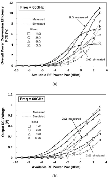
Figure 3.5: Measured and simulated results at 24 GHz. (a) PCE versus Pav, (b) dc voltage versus Pav. ... 33
Figure 3.6: Measured and simulated results at 35 GHz. (a) PCE versus Pav, (b) dc voltage versus Pav. ... 34 Figure 3.7: Measured and simulated results at 60 GHz. (a) PCE versus Pav, (b) dc voltage versus Pav. ... 35 Figure 3.8: Measured PCE results in connection with the transistor and capacitor sizing. ... 38 Figure 4.1: Block diagram of a recently proposed MMID system with a battery-free active tag on single-chip. ... 41 Figure 4.2: Operation principles of the proposed zero-IF SOM. ... 43 Figure 4.3: (a) Zero-IF SOM simplified model, (b) spectrum of the injected RFinj signal during reader-to-tag communication, (c) spectrum of RFinj signal during tag-to-reader communication. ... 44 Figure 4.4: Operating condition of cross-coupled pair transistors when biased close to their threshold voltage and their respective parasitic capacitors. ... 46 Figure 4.5: Zero-IF current and loading condition. ... 51 Figure 4.6: Simulated results that demonstrate the operating conditions of the SOM with and without RFinj signal. ... 54 Figure 4.7: Simulated results of the recovered (down-converted) baseband signal at zero-IF output pad, when an AM signal, modulated by a random signal, is injected into the SOM. ... 55 Figure 4.8: Die microphotograph of the fabricated SOM. ... 58 Figure 4.9: (a) measurement setup, (b) photograph of measurement setup and the probe station. 59 Figure 4.10: SOM phase noise measured at RFout pad for different power levels of the injected RFinj signal. ... 60 Figure 4.11: (a) Spectrum of AM signal, modulated by a 10-kHz square wave signal, and injected into the SOM at RFinj pad (Res BW 4.7 kHz, VBW 4.7 kHz), (b) recovered down-converted baseband signal measured at zero-IF pad. ... 61 Figure 4.12: Measured conversion loss versus injected power for different modulation index. ... 62
Figure 4.13: Measured and simulated conversion loss versus carrier-to-sideband power ratio of the injected RFinj signal. ... 63 Figure 4.14: Measured and simulated conversion loss versus frequency of modulating signal a(t).
... 64 Figure 4.15: Spectrum of SOM measured at the RFout pad, when a 1-MHz sinus wave emulating the tag’s data to be transmitted is injected into the SOM (Res BW 39 kHz, VBW 39 kHz). 64 Figure 4.16: Power link-budget of the proposed MMID tag-reader system. ... 65 Figure 5.1: Illustration of the proposed battery-free active MMID tag in a single-chip with
antenna-in-package: (a) top view, (b) exploded view. ... 69 Figure 5.2: Block diagram of the proposed millimeter-wave identification (MMID) system with a battery-free active tag on single-chip. ... 72 Figure 5.3: Circuit schematic of the power unit management, comprising of a mm-wave/dc rectifier and a low-power voltage regulator. ... 74 Figure 5.4: Circuit schematic of the proposed zero-IF self-oscillating mixer as an MMID tag transceiver. ... 76 Figure 5.5: Simulated results of the power unit management circuit (powering RF signal = 24 GHz @ 10 dBm): (a) start-up and regulated phases as a function of time, (b) rectified and regulated voltage ripples. ... 78 Figure 5.6: Proposed antenna: (a) U-folded coplanar folded dipole, (b) ring slot backed SIW cavity fed by GCPW. ... 79 Figure 5.7: Reflection coefficient |S11| (dB) of the U-folded antenna and ring slot antenna and the
isolation between two ring antennas in a perpendicular configuration. La = 9.5 mm, Lb = 6.84 mm, Lf = 1.16 mm, Rs = 0.58 mm, Rc = 1.065 mm, Ws = 0.025 mm. ... 81 Figure 5.8: Simulated radiation patterns: (a) U-folded dipole antenna, (b) ring slot backed SIW cavity. ... 82 Figure 5.9: The proposed MMID tag with the CMOS die microphotograph. ... 83 Figure 5.10: (a) Measurement setup, (b) photograph of the measurement setup. ... 84
Figure 5.11: Rectified and regulated voltages as a function of RF input power (RF powering signal = 24 GHz) measured at the output of the tag. ... 85 Figure 5.12: Measured spectrum from the tag: (a) when the tag is unlocked (free-running), (b) when the tag is injection-locked by the reader (RFinj ≈ - 30 dBm @ 40 GHz). ... 87 Figure 5.13: Measured phase noise from a free-running and an injection-locked (RFinj ≈ - 30 dBm @ 40 GHz) tag. ... 87 Figure 5.14: (a) Data sent to the tag by the reader @ 100 kbps, by modulating a 40 GHz carrier signal transmitted to the tag, (b) received and demodulated data measured at the output of the tag. ... 89 Figure 5.15: Eye diagram of the recovered data (demodulated by the tag) when the reader sends data at 500 kbps. ... 89 Figure 5.16: (a) Data sent to the reader by the tag @ 10 Mbps, by modulating the injection-locked SOM’s natural oscillation frequency, (b) measured spectrum of the transmitted data from the tag. ... 90 Figure 6.1: Illustration of the proposed single CMOS-die active MMID tag that uses a harvested energy from an incoming mm-wave signal from the reader. ... 95 Figure 6.2: Two MMID system design platforms of choice: (a) AiP-based MMID system reported in [62]; (b) AoC-based MMID system proposed in this work. ... 96 Figure 6.3: Illustration of the proposed rectangular slot antenna on CMOS process. ... 100 Figure 6.4: Illustration of E-field field distributions in the slot region of a rectangular -ring slot antenna: (a) the first resonant mode; and (b) the second resonant mode. ... 101 Figure 6.5: Reflection coefficient |S11| (dB) of the rectangular slot antennas at 24 GHz (La=1.78
mm, Lb=0.89 mm, S= 0.04 mm, WCPW=0.05 mm, SCPW= 0.02 mm, LCPW= 0.16 mm) and 40
GHz (La=1.32 mm, Lb=0.43 mm, S= 0.04 mm, WCPW =0.05 mm, SCPW=0.02 mm,
LCPW=0.39 mm). ... 102
Figure 6.6: Simulated 3D radiation patterns of the dual-band rectangular slot antenna: (a) 24 GHz, (b) 40 GHz. ... 103 Figure 6.7: Illustration of the proposed dual-band rectangular slot antenna on CMOS process. 104
Figure 6.8: Transmission from the common input port to the 40 GHz rectangular slot. ... 104
Figure 6.9: E-field field distributions in the slot region of a rectangular slot antenna: (a) the first resonant mode; and (b) the second resonant mode. ... 105
Figure 6.10: Reflection coefficient |S11| (dB) of the dual-band rectangular slot antenna (La1=1.78 mm, Lb1=0.89 mm, La2=1.32 mm, Lb2=0.43 mm, S=0.04 mm, WCPW=0.05 mm, SCPW=0.02 mm, LCPW1=0.16 mm, LCPW2=0.19 mm). ... 106
Figure 6.11: Simulated 3D radiation patterns of the dual-band rectangular slot antenna: (a) 24 GHz, (b) 40 GHz. ... 107
Figure 6.12: Geometry of the proposed DRA. ... 108
Figure 6.13: Gain .vs. DR thickness Dh. ... 109
Figure 6.14: Gain .vs. DR dimension Dx. ... 109
Figure 6.15: Electric field distribution of the proposed antenna: (a) 24 GHz, (b) 40 GHz. ... 110
Figure 6.16: Simulated 3D radiation patterns of the dual-band rectangular slot antenna with DRA: (a) 24 GHz, (b) 40 GHz. ... 110
Figure 6.17: Radiation measurement setup of the fabricated on-chip dual-band slot antenna (La=1.78 mm, Lb=0.89 mm, S= 0.04 mm, WCPW=0.05 mm, SCPW= 0.02 mm, LCPW= 0.16 mm) and 40 GHz (La=1.32 mm, Lb=0.43 mm, S= 0.04 mm, WCPW =0.05 mm, SCPW=0.02 mm, LCPW=0.39 m) (a) block diagram; (b) die microphotograph of the fabricated antenna without DR; (c) antenna with DR. ... 112
Figure 6.18: Reflection coefficient |S11| (dB) of the antenna (simulated and measured). ... 113
Figure 6.19: Measured and simulated radiation patterns (a) H-plane 24 GHz, (b) H-plane 40 GHz, (c) E-plane 24 GHz, (d) E-plane 40 GHz. ... 115
LIST OF SYMBOLS AND ABBREVIATIONS
AiP Antenna-in-Package AM Amplitude Modulation AoC Antenna-on-Chip ASK Amplitude Shift Keying
BW Bandwidth
CMOS Complementary Metal Oxide Semiconductor CPW Coplanar Waveguide
CW Continuous Wave
DC Direct Current
DRA Dielectric Resonator Antenna EIRP Effective Isotropic Radiated Power FCC Federal Communications Commission GCPW Grounded Coplanar Waveguide
HF High Frequency
HFSS High Frequency Structural Simulator IC Integrated Circuit
IF Intermediate Frequency IoT Internet of Things
LF Low Frequency
LiR Line Regulation LO Local Oscillator LoR Load Regulation
MMID Millimeter-Wave Identification PCE Power Conversion Efficiency
RF Radio Frequency
RFID Radio Frequency Identification
Rx Receiver
SIW Substrate Integrated Waveguide SOM Self-Oscillating Mixer
Tx Transmitter
UHF Ultra-High Frequency VBW Video Bandwidth
LIST OF APPENDICES
CHAPTER 1
INTRODUCTION
The earliest RFID systems were based on quasi-static magnetic flux coupling among the reader's and tag's coils, such as those using low frequencies (from 100 kHz to 2 MHz) or high frequencies (at 13.56 MHz). Later on, radiative (or far-field coupling) RFID systems which permit longer communication links (ultra-high frequencies from 850 MHz to 950 MHz), and microwave frequencies (at 2.45 GHz and 5.8 GHz) were adopted. Recently, RFID technology has been propelled into the millimeter-wave era, to alleviate restrictions that have been limiting the evolution of low-frequency RFID technology [1]. The emerging MMID technology is poised to clearly exploit advantages from operating in this frequency band, therefore circumvents limitations of low- frequency RFID technology. The emerging MMID technology presents several advantages, namely:
At millimeter-wave frequencies, the small effective wavelength makes it possible for a reader to implement a directive and high-gain antenna array [2], and with a beam steering capability, the reader can localize and identify tags one-by-one among a densely deployed MMID tags or sensors with a quasi-laser precision (pinpoint localization). This cannot be made possible with today’s commonly used UHF RFID technology. Besides, at millimeter-wave frequencies, circuit components become smaller, thereby allowing a smaller tag and smaller handheld reader that could even be integrated into our mobile phone [3].
The larger available bandwidth at millimeter-wave frequency and the line of sight communication (a very directive antenna for both reader and tag) enable a highly-secured data exchange between a reader and a tag at a high bit-rate, regardless of the type of modulation and coding. Besides, the losses inherent to millimeter-wave propagation confines the personal data indoor, therefore resolving the primordial issue of security and ethic.
In addition, the still-emerging MMID concept is fully compatible with future applications of millimeter-wave technology in wireless communications and which are being discussed and developed worldwide, such as 5G and IoT (Internet of Things).
1.1 Motivation and Objectives
In addition to the aforementioned advantages of an MMID system, over these millimeter-wave frequency bands the effective wavelength is close to a typical CMOS die size. Therefore, if antennas could either be integrated on the same chip (antenna-on-chip –AoC) or embedded in the associated package (antenna-in-package –AiP), and assuming that energy could be wirelessly and efficiently harvested at millimeter-wave frequencies so as to allow a tag transmit its data to a reader at millimeter-wave frequencies, it becomes possible then to envisage a complete MMID tag that is fully integrated on a single CMOS die. The development of this new generation of high data-rate, battery-free, yet active μRFID technology with full on-chip integration operating at mm-wave frequencies has been the motivation for this Ph.D. thesis work. Accordingly, the main goal of this thesis is fourfold:
Propose and analyze an architecture of an MMID system (reader-tag) that addresses the underlying technical challenges and fully benefits from the advantages of operating at millimeter-wave frequencies.
Propose, analyze, and develop techniques to efficiently convert an RF energy (at millimeter-wave frequencies) into a DC energy.
Propose, analyze, and develop ultra-low-power millimeter-wave transceivers that could only rely on a harvested energy to operate.
Develop and demonstrate a high data-rate, single-chip, battery-free, yet active MMID tag, exploring two major solutions (antenna-in-package and antenna-on-chip) for highly integrated millimeter-wave systems.
Since the tag cost represents the main factor that limits a widespread adoption of a new technology, a standard, low-cost, and commercially available CMOS process with a high integration capability is the process of choice, regardless of the significant design challenges in achieving the desired performances, especially in the scope of millimeter-wave integrated circuits design.
1.2 Contribution and Organization of the Thesis
This thesis is written in articles-based format, and all the chapters are organized as follow:
Chapter 1: Introduction
This chapter introduces the millimeter-wave identification technology and its potential advantages, and highlights the thesis work’s motivation, objectives, contribution, and its organization.
Chapter 2: Literature review
This chapter reviews the key notions of RFID technology, wireless power harvesting techniques using CMOS circuits, and the millimeter-wave identification (MMID) technology.
Chapter 3 Article 1: High-Efficiency Wideband Rectifier for Single-Chip Batteryless Active Millimeter-Wave Identification (MMID) Tag in 65-nm Bulk CMOS Technology
This chapter demonstrates that RF energy at millimeter-wave frequencies can be wirelessly harvested and converted into DC energy, with power conversion efficiencies that were never demonstrated before at such frequencies. Starting from a differential-driven cross-coupled rectifier topology that was demonstrated to work at UHF frequencies only, we have investigated its characteristics and performances at 24 GHz, 35 GHz and 60 GHz. In order to achieve high conversion efficiency, we have then redesigned and optimized its circuit parameters and the chip layout specifically for these millimeter-wave bands. This has been demonstrated through an implementation using a standard commercially available CMOS technology. This chapter also proposes a new MMID reader-tag system architecture that addresses and solves the underlying technical challenges associated to commonly used passive RFID systems.
Chapter 4 Article 2: Low-Power Injection-Locked Zero-IF Self-Oscillating Mixer for High Gbit/s Data-Rate Battery-Free Active RFID Tag at Millimeter-Wave Frequencies in 65-nm CMOS In this chapter, an extremely low-power millimeter-wave transceiver that relies only on harvested energy for its power supply, is proposed and demonstrated in 65-nm standard CMOS technology. The transceiver is based on a self-oscillating mixer architecture, which we have improved through key circuit topology modifications and design considerations. Our transceiver is capable, on one hand (during reader-to-tag communication) to receive an AM-modulated signal at mm-wave frequency and to down-convert to baseband signal without any external local oscillator nor an IF stage, which results in minimal current consumption. On the other hand (during tag-to-reader communication), the same self-oscillating mixer directly up-converts a high-data-rate binary signal into the millimeter-wave band.
Chapter 5 Article 3: High-Data-Rate Single-Chip Battery-Free Active Millimeter-Wave Identification Tag in 65-nm CMOS Technology
This chapter demonstrates a miniaturized (10 x 10 mm2) high-data-rate, self-powered, yet active
MMID tag on a single-chip. The tag wirelessly harvests its energy at millimeter-wave frequency, receives an interrogator signal at millimeter-wave carrier frequency (and it is assumed that in the intended application data is then written in the tag), and transmits back its data at high-bit-rate to a reader on a millimeter-wave carrier frequency as well. The tag’s antennas are embedded in the package (antenna-in-package).
Chapter 6 Article 4: On-Chip Dual-Band Rectangular Slot Antenna for Single-Die Millimeter-Wave Identification Tag in Standard CMOS Technology
In this chapter, we address and tackle the well-known drawbacks of silicon-based integrated antennas, which are the antenna’s radiation efficiency and silicon required surface. A dual-band and high-efficiency rectangular slot antenna is demonstrated using a standard bulk CMOS process. The demonstrated antenna supports the feasibility of a fully integrated MMID tag on a single CMOS-die (a CMOS-only MMID tag), with no external components whatsoever.
Chapter 7: General Discussion
This chapter provides a general discussion on potential applications and novel opportunities enabled by our research in this thesis.
Chapter 8: Conclusion and Future Works
This chapter concludes the thesis with a brief highlight of the achieved results and suggests some areas in which future extensions of this work could be targeted.
CHAPTER 2
LITERATURE REVIEW
This chapter reviews the key notions of RFID technology, wireless power harvesting techniques using CMOS circuit platforms, and the millimeter-wave identification (MMID) technology.
2.1 RFID Technology
Interrogator signal from the reader
Data from the tag
RFID Tag
Server RFID Reader
Figure 2.1: Illustration of an RFID system.
Among many other identification technologies, RFID, which has widely impacted our everyday life in many areas, is a technology that uses radio communications to wirelessly and automatically identify objects or people. A typical RFID system is generally a two-way communication system (figure 2.1), where a base station (called a reader or an interrogator), wirelessly exchanges data with a device (called a tag or a transponder) which is attached to the object or the people to be identified [4]. Readers are generally complex and connected to a host computer or a network, whereas transponders target simplicity, low-price, and small size (generally use integrated circuits) for a widespread adoption and a massive-use of the technology.
2.1.1 Different types of RFID
RFID systems are essentially categorized by the way power is supplied to the tag, by the protocols used for communication between the tag and the reader, and by the operating frequency as well. The choice of frequency, power source, and protocol greatly affects the cost, communication range, tag size, data security and features available to the user, etc., which generally influence how the RFID technology is adopted and spread into the market.
2.1.1.1 Active RFID
Logic Circuit
Filter Amp Mixer
Battery RF Block Vdd Out In VCO Tag Filter Filter Amp Amp Mixer Transmitted data Interrogator signal Server Reader
Figure 2.2: A general representation of a typical active RFID system.
As illustrated in Fig. 2.2, which depicts a general representation of a typical active RFID system, an active RFID tag is nothing else than a conventional bidirectional radio communication device, with its own power source, conventional transceiver, sensors, memory, a digital processing block, etc. Active tags are the most expensive and are often used for specialized applications where tracking or locating objects requires a long range of communication (tens or hundreds of meters), a high security data-exchange, and an environment where the reader-tag path is obstructed (no line of sight from a reader to tag). They are, for example, commonly used for tracking shipping
containers, and they are able to discriminate one container from another even when containers are in close proximity to one another.
2.1.1.2 Passive RFID Server Reader Tag Backscattered data Interrogator signal + Energy Logic Circuit Vdd Out In RF/DC Rectifier Envelope detector Interrogator signal RF signal for power supply Modulator
Figure 2.3: A general representation of a typical passive RFID system.
Figure 2.3 illustrates a simplified representation of a typical passive RFID system (in reality, a passive RFID tag could be more sophisticated than this representation). Unlike the active RFID tag, a passive RFID tag does not have an independent power source nor a dedicated radio transceiver. The tag rectifies the RF signal received from the reader to recuperate its energy and power up its logic and non-volatile memory circuitries. The tag responds back to the reader (sending its data to the reader) by modifying its antenna’s impedance seen by the reader (backscattering modulation technique). In figure 2.3, the modulator is conceptually represented by a simple switch. By switching on/off the modulator as a function of the digital data to be sent, it
changes the electrical characteristics of the antenna in a way that the reflected signal from the antenna is analogously an AM-modulated signal.
Since passive RFID tags have neither radio transceiver nor any dedicated power source, they are relatively simple in terms of manufacturing cost and complexity, they are small, and therefore are low cost devices without any related maintenance fees (they could be deployed in a hostile or less accessible environment). However, their simplicity comes with some disadvantages: a) Communication range is greatly limited by the capability of the tag to harvest sufficient energy for its logic and memory circuitries (the sensitivity of the rectifier circuit). This limitation is particularly proportional to the operating frequency since propagation losses increase with frequency.
b) Since the tag relies on the rectified power, computational power must be minimized and the tag must be designed in a way to use very little of the rectified power. Therefore, integration of sensors and functionalities are limited by the limited power budget and the reader uses very simple protocols to communicate with the tag.
c) Limited energy resources (limited computational power) greatly affects security and privacy as well, since it limits the capability to implement different coding techniques in order to improve the security of the exchanged data between the reader and the tag.
Link power-budget for a typical passive RFID system
Figure 2.4: Link power-budget for a typical passive RFID system [4].
Figure 2.4 provides a more detailed communication range analysis. A passive RFID system has two principal constraints limiting its operation: the power transferred to the transponder and the power received by the reader. The system has two critical power levels, the transponder sensitivity and the reader sensitivity (the minimum power levels required by the transporter and the reader). As illustrated in figure 2.4, the operating range is a smaller range between uplink (tag-to-reader) and downlink (reader-to-tag) communication range. It is in fact set up by the downlink communication range, because for a wirelessly powered tag (passive RFID system), the operating
range is limited by the capacity of a tag to harvest sufficient energy for its circuitry (downlink), rather than the reader’s sensitivity (uplink) which is generally very good (low power level).
Limitations of a real free-space communication environment
Figure 2.5: Realistic environment of a passive RFID system [4].
As discussed above, in a backscattering passive RFID system, a reader continuously sends a high power signal to power up the tag, while listening to a very weak reflected signal, sent by the tag as a result of the impedance-switching of its own antenna. However, as depicted in figure 2.5 where a real environment is full of reflectors, the total received signal by the reader consists not only of the wanted signal that carries the tag information, but also the reader’s transmitter leaked signal (self-jamming), the signal reflected by the transmitter’s own antenna, and other reflected signals from surrounding objects. The signal that comes from the leakage (coupling between the reader’s transmitter and the reader’s receiver) dominates the overall noise at the receiver side. This negatively impacts the reader sensitivity, and the phenomenon is more severe for higher operating frequency (the higher the operating frequency goes, the worse the isolation between the reader’s transmitter and the reader’s receiver becomes).
2.1.1.3 Semi-Passive RFID Tag Backscattered data Interrogator signal Logic Circuit Vdd Out In Envelope detector Interrogator signal Modulator Battery Server Reader
Figure 2.6: A general representation of a typical semi-passive RFID system.
As illustrated in figure 2.6, a semi-passive tag is a battery-assisted passive tag. It has a dedicated battery to power up the tag’s circuitry, but, like passive tag, it still uses backscattering modulation technique for uplink communication (tag-to-reader communication). It also does not have a radio transmitter. Since it incorporates a power source, a semi-passive tag could integrate more functions and extend the communication range (a communication distance of about 100 meters is feasible). It is more likely to respond at such distances, compared to its passive tag counterpart which relies on the rectified energy. Therefore, semi-passive tags are used in dedicated applications such as tracking high-value assets where missing a tag (a tag does not respond) cannot be tolerated. Reliability is privileged over an increase in tag size due to battery or the maintenance related cost.
2.1.1.4 Chipless RFID
Unlike the commonly used RFID tags, chipless RFID technology does not incorporate a digital logic circuit, therefore suffering from the inability to write data to the tag. In some chipless RFID applications, surface-acoustic wave (SAW) devices and electromagnetic resonant techniques are used. However, it worth noting that the cost of printing technologies is considerably higher than that of silicon manufacturing, for the same complexity. In high volume production, it is cheaper to fabricate a circuit on silicon than to print it directly onto a PCB substrate. Besides to the lack of flexibility of the kind that exists with a digital logic circuit (a CMOS IC), manufacturing cost seems to be the main factor that limits the evolution and a wide-spread adoption of the chipless RFID technology. It is now limited to some specialized applications.
2.1.2 RFID Operating Frequency Bands
Figure 2.7: RFID frequency bands [4].
With today’s wireless communication explosion, RFID technology should fairly cohabit with other wireless systems without interference. Note, for example, in the 860-960 MHz band an RFID system should directly cohabit with cellular telephony and other popular wireless systems
operating in this crowded band. As illustrated in figure 2.7, the most commonly used frequency bands which have been made available by regulatory agencies (FCC for USA, CRTC for Canada) are the 125/134 kHz (low-frequency: LF), 13.56 MHz (high-frequency: HF), 860–960 MHz (ultra-high-frequency: UHF), 2.4–2.45 GHz (UHF or microwave), and 5.2–5.8 GHz (microwave band). These restricted narrow bands have mostly been made available for unlicensed ISM (industrial, Scientific and Medical) activities. Low-frequency RFID systems are generally inductively coupled and limited to low data rate with a short communication range, whereas UHF RFIDs are radiative and provide a higher data rate, longer communication range, and smaller tag size.
2.1.3 RFID Tags Implemented Using CMOS Technology
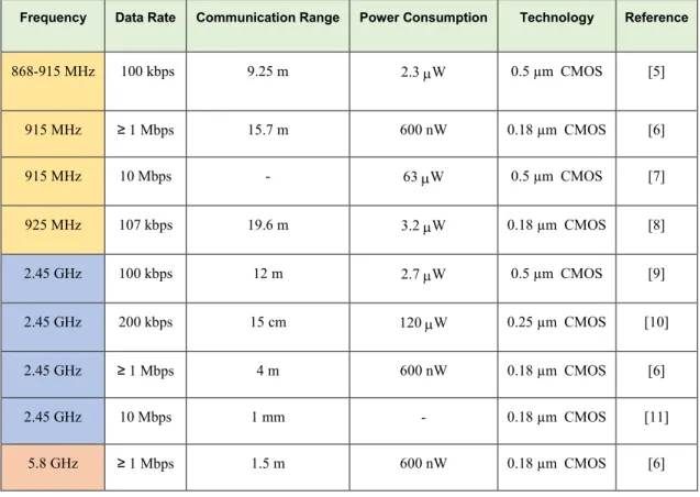
With the extensive use of RFID technology together with a relentlessly declining DC power consumption in the novel integrated circuits, integrating micro- or nano-sensors that implement novel functionalities and decisional algorithms (digital signal processing) prompts new classes of RFID technology. To deploy a large number of those sensors or tags, however, requires a cost- and integrability-effective fabrication process. A standard, low-cost, and commercially available CMOS process with a high integration capability is the process of choice for a widespread adoption and massive applications of RFID technology. Recently published work’s performances are summarized in Table 2.1.
Table 2.1: Performance summary of UHF/microwave passive RFID tags in CMOS technology.
Frequency Data Rate Communication Range Power Consumption Technology Reference
868-915 MHz 100 kbps 9.25 m 2.3 W 0.5 µm CMOS [5] 915 MHz ≥ 1 Mbps 15.7 m 600 nW 0.18 µm CMOS [6] 915 MHz 10 Mbps - 63 W 0.5 µm CMOS [7] 925 MHz 107 kbps 19.6 m 3.2 W 0.18 µm CMOS [8] 2.45 GHz 100 kbps 12 m 2.7 W 0.5 µm CMOS [9] 2.45 GHz 200 kbps 15 cm 120 W 0.25 µm CMOS [10] 2.45 GHz ≥ 1 Mbps 4 m 600 nW 0.18 µm CMOS [6] 2.45 GHz 10 Mbps 1 mm - 0.18 µm CMOS [11] 5.8 GHz ≥ 1 Mbps 1.5 m 600 nW 0.18 µm CMOS [6]
2.2 Wireless Power Harvesting with CMOS-based Rectifier Circuits
2.2.1 Conventional Diode-Connected Transistor
One stage
Figure 2.8: Wireless power harvesting using a CMOS-based voltage multiplier [12].
For a commercially available standard CMOS process, a conventional diode-connected transistor plays the role of the rectifying element such as its counterpart Schottky diode. As illustrated in figure 2.8, a voltage multiplier structure is the commonly used technique to boost the rectified voltage. As highlighted (figure 2.8), a one stage (a full-wave rectifier) consists of two diode-connected transistors M1 and M2, and two capacitors C1 and C2. In its negative phase, the incoming RF signal Vin swings below some reference voltage (VRef) minus the transistor’s
threshold voltage Vth1 and the transistor M1 turns on, allowing the current IM1 to flows from ground
(or some VRef ) into capacitor C1. In the positive phase and when Vin > Vth2, transistor M2 turns on
and current IM2 flows from C1 to C2. As long as an RF source is connected to the rectifier, the
across the output node. High threshold voltage Vth of diode-connected transistors significantly
degrades the rectifier’s sensitivity (conventional diode-connected transistors are not suitable for small RF signals or long communication range).
2.2.2 Power-Matching and Voltage Gain-Boosting Network
(a) (b)
Figure 2.9: Passive voltage-boosting network: (a) using an LC-resonator, (b) using a step-up transformer [13].
It is clear that to boost the power conversion efficiency of the voltage multiplier, both the power matching (between the antenna and the voltage multiplier) must be optimized and the amplitude of the voltage from the antenna must be maximized.
As illustrated in figure 2.9 (a), an LC network impedance transformer is inserted between the antenna and the multiplier. The LC network provides a matching impedance to the antenna in order to maximize the power transmission from the antenna to the voltage multiplier. At the same time, by resonating at the carrier frequency, the voltage at the output of the LC network (the input of the multiplier) is maximized, therefore enhancing the overall power conversion efficiency. The topology in Figure 2.9 (b) takes advantages offered by a step-up transformer, to simultaneously provide a power-matching and a voltage gain-boosting. With a step-up transformer, the same power can be delivered from the primary winding to the secondary winding, but with a higher voltage at the secondary winding.
The LC-based and the step-up transformer-based impedance transformer networks are limited by the low quality factor of spiral inductors in standard CMOS technologies.
2.2.3 External Threshold Voltage Cancellation
(a)
(b)
Figure 2.10: Diode-connected transistor rectification mechanism: (a) without external bias, (b) with external bias [14].
Figure 2.11: I-V curve of a diode-connected transistor with/without external bias [15].
As illustrated in figure 2.10 (b), in this approach, a bias voltage Vbth is connected between the gate
G and drain D terminals of each transistor. Therefore, the effective threshold voltage decreases from Vth to Vth-Vbth, thereby increasing the rectifier’s sensitivity (the rectifier can detect and rectify
small incoming RF signals: for long-distance communication). The rectified current increases with the bias voltage. However, when the source voltage becomes greater than the drain voltage, due to the MOS transistor symmetrical structure, diode-connected transistors suffer from a reverse leakage current (figure 2.11) that discharges the output capacitor, therefore degrading the overall power conversion efficiency. Besides, this technique could only be applied in an active or a semi-passive tag, since Vbth itself has to be externally generated.
2.2.4 Zero-Threshold Voltage Transistors (native transistors)
Lower transistor’s threshold voltage enhances power conversion efficiency, since it presents a low turn-on resistance. Therefore, some rectifiers are implemented using low-threshold or zero-threshold voltage transistors models, generally called native transistors. These models are available in some standard CMOS processes. However, leakage current increases exponentially with the decrease of the transistor’s threshold voltage Vth, resulting in the suppression of the increase in
power conversion efficiency PCE. Finally, a rectifier using very low-Vth or near-zero threshold
voltage (native) transistors perform much better at lower RF power values (small turn-on voltage), but as the input power rises further, they perform poorly because of leakage current.
2.2.5 Cross-Coupled Differential-Drive Topology
(a) (b)
Figure 2.12: Circuit schematic of a cross-coupled differential-drive rectifier: (a) conventional topology [15], (b) improved topology [16].
As previously mentioned, a static gate bias voltage increases the rectifier’s sensitivity compared to the simple diode-connected transistor without any external gate-biasing. As illustrated in figure 2.11, static biasing also increases reverse leakage current, therefore degrading the overall power conversion efficiency, especially as the received RF power increases. However, the cross-coupled topology shown in figure 2.12 addresses this on-resistance and leakage current trade-off. Since the rectifier is differentially driven, reverse leakage current is minimized by a negative gate voltage. Therefore, both smaller on-resistance and smaller reverse leakage current are simultaneously obtained. With a modified topology (figure 2.12 (b)), leakage current is greatly reduced or ideally suppressed, thereby allowing high efficiency over a wide dynamic range of input power. This relates to realistic operating conditions of the tag, where the distance between a reader and a tag may vary at any time, which automatically introduces a variation in the received power. Table 2.2 summarizes and compares performances of the previous published CMOS rectifiers using different techniques to enhance both power conversion efficiency and the rectifier’s sensitivity.
Table 2.2: Performance summary of CMOS rectifiers using different rectification techniques.
Rectifier Technique Frequency Sensitivity Output DC Power Efficiency Technology Reference
Diode-Connected Transistors 900 MHz -7.0 dBm 2.4 µW (0.4 V @ 6 µA) 1.2 % 0.25 µm CMOS [17] Voltage Gain-Boosting Network 3.85 GHz -12.0 dBm 2 µW (1 V @ 2 µA) 3.0 % 0.18 µm CMOS [13] External Threshold Voltage Cancellation 950 MHz -14.0 dBm 0.6 µW (1.5 V @ 0.4 µA) 1.5 % 0.3 µm CMOS [14] Zero-Threshold Voltage Transistors 900 MHz -11.0 dBm 5 µW (1 V @ 5 µA) 6.5 % 0.18 µm CMOS [18] Cross-Coupled differential-drive Topology 953 MHz -10.0 dBm 65 µW (1.8 V @ 36 µA) 65 % 0.18 µm CMOS [15]
2.3 Millimeter-Wave Identification (MMID) Technology
Recently, some works in MMID technology have been published and none of them has experimentally demonstrated a complete MMID system that fully takes advantages of operating at mm-wave band.
2.3.1 Chipless MMID tag
In [20], a chipless MMID tag at 30 GHz is presented. The chipless tag encodes data into the spectral signature using a multi-resonator. A circuit with 6 spiral resonators and two cross-polarized transmitting and receiving circular UWB monopole antennas is presented. The results shown are not supported by any experimental data and the simulation results show a large spectral use from 24 to 36 GHz (2 GHz by bit). In [21], a 6-bit mm-wave chipless tag is proposed. The tag comprises
two orthogonally polarized slot loaded circular patch antennas, which are connected by a right angle transmission line. The slot on the patch determines the individual resonant frequency signatures, hence the number of identification data bit. However, density of the coding still small (1.6 GHz by bit). In [22], an equalization method is used in order to maximize the number of encoded bits in time-domain reflectometry (TDR) tags. The designed SIW tag is comprised of 4 symmetrical iris in H-plane with integrated slot-antenna. The reader should be used to read code information from a tag with one or more modulation types (phase, polarization, frequency and time domain) in order to yield a significant enhancement of bit density.
2.3.2 MMID tag with integrated chip
In [23], for example, a standard UHF RFID chip is combined with external mixers to up-convert the transmit-UHF signal to 10 GHz and down-convert the received 10 GHz signal to the UHF, with a 40kbit/s data rate. In [24], a 60 GHz RFID tag design is published, but a low RF-to-DC power conversion efficiency (1.2% at 2dBm input power) translates into a bit-by-bit sequential communication, limiting the data rate to only 5kbit/s at a communication range of 1.3 cm.
CHAPTER 3
ARTICLE 1: HIGH-EFFICIENCY WIDEBAND
RECTIFIER FOR SINGLE-CHIP BATTERYLESS ACTIVE
MILLIMETER-WAVE IDENTIFICATION (MMID) TAG IN 65-NM
BULK CMOS TECHNOLOGY
Pascal Burasa, Nicolas G. Constantin, and Ke Wu
Published in the IEEE Transactions on Microwave Theory and Techniques, vol.62, no. 4, pp.
1005-1011, Apr. 2014
This paper presents the development and demonstration of a high-efficiency rectifier for millimeter-wave (or mm-wave)-to-dc energy conversion. It is a critical circuit block that renders possible the use of a single CMOS chip die with no substrate and wiring, as the implementation of a batteryless, yet active tag for next generation high data-rate mm-wave identification (MMID) technologies. We also propose an architecture of Reader-Tag system that addresses the underlying technical challenges. The rectifier is based on a differential drive cross-coupled topology that has been shown to work at UHF frequencies only so far. In this paper, we investigate significant challenges in implementing this topology at mm-wave frequencies with good power conversion efficiency (PCE). The analyses, design and results presented in this work demonstrate the feasibility of achieving this by minimizing simultaneously the small on-resistance and the reverse leakage current in the MOS transistors, and by reducing losses and parasitic capacitances through proper transistor sizing and layout optimization. Using a standard 65-nm bulk CMOS process, a chip was designed, fabricated, and tested under different input and output loading conditions. The rectifier exhibits an overall PCE of 20% at 24 GHz, 18% at 35 GHz, and 11% at 60 GHz under RF available driving power of 6, 6, and 3 dBm, respectively, and output load resistance of 1, 1, and 2 kΩ, respectively. These PCE performances at mm-wave frequencies have never been reported in the literature.
3.1 Introduction
As an emerging technology, Radio Frequency Identification (RFID) is being increasingly used in many areas of our everyday life, such as access control, security, and supply chain management. However, the restricted standard rules, the tag size (mainly dominated by antenna), and limited data rate dictated by available bandwidths, have impeded the evolution of the UHF RFID applications. Driven by the ever-increasing needs, such as smaller size and higher data rates, RFID technology has entered into the mm-wave era to exploit the inherently smaller antenna size and larger available bandwidths [19]. Batteryless MMID becomes only possible if a tag can be powered wirelessly and it still benefits from these advantages at mm-wave frequencies. However, to the best of our knowledge, such MMID has not been reported yet. In [23], a standard UHF RFID chip is combined with external mixers to up-convert the transmit-UHF signal to 10 GHz and down-convert the received 10 GHz signal to the UHF, with a 40-kbit/s data rate. In [24], a 60 GHz RFID tag design is reported, but the low RF-to-dc PCE (1.2% at 2dBm input power) translates into a bit-by-bit sequential communication, limiting the data rate to 5 kbit/s at a range of 1.3 cm.
Vdd Logic + Memory Tag Rectifier Reader Data Recovery PA fRF TX Rx A B Detector 10 100 11 fRF Data coupling with point A Modulator
Figure 3.1: Illustration of a reader-tag RFID system using backscattering.
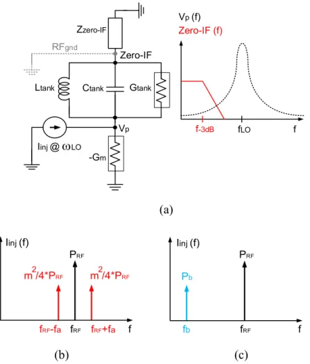
A major challenge in developing a passive MMID is that the backscattering modulation technique generally used in passive UHF RFIDs performs poorly at mm-wave frequencies. As depicted in Fig.3.1, in a backscattering passive RFID system, a reader continuously sends a high power signal to power up the tag, while listening to a very weak reflected signal, sent by the tag
with a form of amplitude modulation as a result of the impedance-switchingofitsownantenna.The signalreceivedbythereaderconsistsoftwosidebandscarryingthetaginformation,andacarriertone levelthatisaugmentedbythereader’stransmitterleakagesignalanditsassociatedside-bandnoise. Thisimpactsnegativelythereadersensitivity,butisacceptableinUHFRFIDs.However,theweaker backscatteredsignalatmm-wavefrequencies(duetosmallertag-antennaaperture),aswellaslower readerTX-RXisolation,higherphasenoiseinitsmm-waveoscillatorandlowreaderdynamicrange [24]compromisethismodulationtechniqueatmm-wavefrequencies. Therefore, batteryless “active” MMID technologies will benefit from a new reader-tag system that is free of backscattering.
In section II of this paper, a new MMID reader-tag system that is free of backscattering modulation is proposed at a conceptual level. The successful implementation of such a system, however, will require mm-wave-to-DC rectifiers with good PCE performances, e.g., ~ 10% at 35 GHz under an RF input power of 6 dBm. To the best of our knowledge, a CMOS rectifier with such performances has never been reported in the literature. Note that published papers on mm-wave rectennas (e.g., [25]-[29]) make use of Schottky diodes and are intended for operation at significantly higher power levels than what is required in our applications.
In section III, we analyze and describe the design of a rectifier that was successfully tested using a commercial standard 65-nm CMOS process, with measured PCE performances of 20%, 18%, and 11% at 24, 35, and 60 GHz, respectively. Section IV presents and discusses the measurement results.
3.2 Proposed MMID System with Batteryless Tag
The MMID reader-tag system proposed for batteryless “active” MMID tags, which does not require backscattering, is illustrated in Fig.3.2. It uses two mm-wave frequencies, freq-1 for a continuous wave (CW) dedicated to energy source for the tag, and freq-2 for down and up-link communications only. Therefore, the reader interrogates and listens to the tag at any time without interrupting the energy feed to the tag, hence without compromising the rectifier’s PCE. Moreover, it eliminates the issue of charging and discharging synchronization stated in [24], as well as the
issue of a reader sensitivity degradation associated with backscattering. This leads to a more relaxed coding and modulation methods, as well as higher data rates in both communication links.
Command Data Transmitted Data Vdd Application ( Memory, Processor, Sensor,...) MMID Tag (On-Chip)
Clock generator Data_out CLK Data_in Mm-wave Transmitter Mm-wave Receiver Millimeter-Wave-to-DC Rectifier MMID Reader Command Data Power Amplifier mm-wave freq-2 mm-wave freq-1 TX antenna Tx/Rx antenna RX antenna Tx/Rx antenna Power 1 01 1 1 01 10 01 01 10 1 Data Recovery
Figure 3.2: Block diagram of the proposed MMID system with a batteryless active tag on single-chip.
Previous works have reported mm-wave CMOS VCOs with power consumption of few hundreds of micro-watts despite a large tuning range [30], a dual-band on-chip antenna with 7.4 and 6.5 dBi gain at 35 and 94 GHz, respectively [31], and a clock generator consuming only 24nW at 5.12 MHz [32]. Besides, at UHF, the state-of-the art has shown fully-integrated passive RFID transponders (including control logic and memory blocs) consuming less than 3 µW dc power [33], [34]. Assuming a 1 W effective isotropic radiation power (1 W EIRP) from a reader, a tag antenna gain of 6 dBi [31], and a conservatively high dc power of 500 µW dissipated by the MMID tag (excluding the rectifier), then a power link budget analysis at 35 GHz using Friis equation shows that a 10% PCE is required for the rectifier to enable communication over 2 cm. With the design presented in this paper, we have measured a PCE of 18% at 35 GHz. This renders possible MMID systems as in Fig. 3.2, employing a batteryless “active” tag that is fully integrated on a single CMOS die, with no substrate, no die-attach and no wiring.
3.3 Millimeter-Wave-to-DC Rectifier
Fig.3.3 (a) shows the rectifier schematic, based on a cross-coupled bridge topology that has been investigated at UHF only so far [15]. It is driven by a differential input signal V_RF applied across nodes Vin_rf+ and Vin_rf-. During the positive cycle of V_RF, and as the difference between Vin_rf+ and Vin_rf- swings above transistors’ threshold voltage Vth, pulsed currents IM3_pos and IM2_pos circulate through M3 and M2. The resulting current equals the fluctuating charge-current through Cload plus the dc current drawn by the MMID tag. In the negative cycle of V_RF, Cload is charged by IM4_neg and IM1_neg. As long as an RF source is connected to the rectifier, transistors M1, M2, M3, and M4 will periodically charge Cload, and a dc voltage develops across the MMID tag.
M1 M2 Vin_rf+ M4 M3 V_RF-V_RF+ Vin_rf-Ca Cb Cload I_DC Rs1 Rs2 MMID Tag M1 M2 Vin_rf+ M4 M3 V_RF-V_RF+ Vin_rf-Ca Cb Cload VDC_A Rs1 Rs2 VDC_B C_pad C_pad C_in I_RF C_pad IM 3_ po s IM 2_ po s IM 1_ ne g IM 4_ ne g V_RF (a) (b)
Figure 3.3: Cross-coupled bridge configuration CMOS rectifier used in this paper. (a) Differential-drive circuit schematic, (b) Equivalent capacitor model.
The cross-coupled bridge topology allows a small on-resistance by biasing the NMOS (M2) in the saturation mode, with a high gate voltage during the positive cycle of V_RF. It also allows reducing the unwanted Source-to-Drain reverse leakage current in M2 (due to the MOS
symmetrical structure) during the negative cycle of V_RF by pulling down this transistor’s gate voltage.
The same mechanisms in opposite cycles of V_RF apply for the other NMOS and the PMOS transistors, resulting into high PCE at UHF. At mm-wave frequencies, though, parasitic capacitances and series losses associated with Ca, Cb, and Cload capacitors dominate and degrade significantly the PCE. This will be analyzed in the following, with the help of formulations from [18].
As shown in Fig.3.3 (b), at mm-wave frequencies, the cross-coupled bridge topology implies a large parasitic capacitor C_in that reduces the differential voltage, and the transistors operate in weak-inversion region (higher channel resistance), resulting in a low PCE. Cload is then charged by a weak sub-threshold current defined by (3.1)
𝐼𝑠𝑢𝑏 = 𝐼𝑠𝑜.𝑊𝐿 . 𝑒𝑉𝑔𝑠⁄𝑛𝑉𝑇(1 − 𝑒−𝑉𝑑𝑠⁄𝑉𝑇). (1 + 𝜆 𝑠𝑢𝑏𝑉𝑑𝑠) (3.1) with 𝐼𝑠𝑜 = μ√𝑞𝜖𝑠𝑖𝑁𝑐ℎ 2𝜙𝑠 . (𝑉𝑇) 2. 𝑒(−𝑉𝑡ℎ−𝑉𝑜𝑓𝑓) 𝑛𝑉⁄ 𝑇 (3.2)
where 𝑞 is the electron charge, 𝜖𝑠𝑖 is the silicon permittivity, 𝑁𝑐ℎ is the doping concentration, 𝜙𝑠 is the surface potential, 𝑉𝑇 is the thermal voltage, 𝜆𝑠𝑢𝑏 is the sub-threshold region channel-length
modulation parameter, 𝑉𝑜𝑓𝑓 is the sub-threshold region offset voltage, 𝑉𝑡ℎ is the threshold voltage,
𝑛 is the sub-threshold region swing parameter, 𝑊 is the transistor width, 𝐿 is the transistor length, and μ is the electron mobility.
C_in = {C_in(𝑛𝑒𝑔) = 𝐶C_in(𝑝𝑜𝑠) = 𝐶𝑔𝑠2(𝑜𝑛)+ 𝐶𝑔𝑠3(𝑜𝑛)+𝐶𝑔𝑠1(𝑜𝑓𝑓)+𝐶𝑔𝑠4(𝑜𝑓𝑓) 𝑔𝑠2(𝑜𝑓𝑓)+ 𝐶𝑔𝑠3(𝑜𝑓𝑓)+𝐶𝑔𝑠1(𝑜𝑛)+𝐶𝑔𝑠4(𝑜𝑛) (3.3) with, {𝐶𝑔𝑠(𝑜𝑛) = 2 3. 𝜀𝑜𝑥 𝑡𝑜𝑥. 𝑊. 𝐿 𝐶𝑔𝑠(𝑜𝑓𝑓)=𝜀𝑜𝑥 𝑡𝑜𝑥. 𝑊. 𝐿𝑑𝑖𝑓𝑓 (3.4)
where 𝜀𝑜𝑥,𝑡𝑜𝑥, and 𝐿𝑑𝑖𝑓𝑓 are the oxide dielectric constant, the oxide thickness, and the channel
length diffusion, respectively. To minimize C_in (3.4), smaller transistor width 𝑊 should be used. However, smaller 𝑊 also decreases saturation current 𝐼𝑠𝑎𝑡 (3.5), consequently decreasing Cload
charge-current and the PCE.
𝐼𝑠𝑎𝑡 =12𝜇𝐶𝑜𝑥(𝑊𝐿) (𝑉𝑔𝑠− 𝑉𝑡ℎ)2 (3.5)
Larger transistor 𝑊 enhances 𝐼𝑠𝑎𝑡 (3.5), but larger 𝑊 increases both parasitic capacitances (3.4) and leakage current (3.6), thus degrading PCE (charges leak away). On the other hand, a higher loading current (500 µA as targeted for the novel MMID tag) requires large-enough Cload and transistor widths. Larger capacitors Ca, Cb, and Cload imply higher losses, severely degrading PCE.
𝐼𝑙𝑒𝑎𝑘 = 𝐼𝑠𝑜.𝑊𝐿 . (1 − 𝑒−𝑉𝑑𝑠⁄𝑉𝑇). (1 + 𝜆
𝑠𝑢𝑏𝑉𝑑𝑠) (3.6)
Moreover, a low 𝑉𝑡ℎ is beneficial to 𝐼𝑠𝑎𝑡 (3.5), but also implies a larger leakage current
(3.6). Finally, a longer channel implies more parasitic capacitance (3.4), making the minimum usable 𝐿 the best design choice.
The above-described complex design trade-offs show that a performant mm-wave rectifier design necessitates a thorough optimization. In this work, we aimed at optimizing the rectifier’s PCE by simulation for best transistor and capacitor sizes, as a function of the loading current. Note however, that since a rectifier is a large-signal nonlinear circuit, a more robust optimization actually requires a much more complex procedure, such as what was proposed in [35], where source-pulling characterization is employed.
Our simulations showed that minimal transistor sizes yield an optimal design choice for our mm-wave rectifier. In addition, layout parasitic capacitances are critical for PCE. Hence, the distances between polysilicon gate, source, and drain contacts were optimized to reduce 𝐶𝑔𝑠,𝐶𝑔𝑑, and 𝐶𝑑𝑠.
In order to minimize capacitive coupling between metal traces, together with the associated losses, the transistors may be kept further apart to allow more distance between the metal traces. On the other hand, too long metal traces severely degrade the PCE because of excessive substrate losses. This aspect was taken into consideration during the layout design, through multiple iterations of post-layout simulation.
Series resistances Rs1 and Rs2 (Fig. 3.3) were added for test purposes, in order to isolate the small Cload capacitor from the bigger and lossy parasitic capacitors in the test pads. Rs1 and Rs2 ensure that the RF signal flows through Cload, rather than C_pad or being radiated by the probe cable.
![Figure 2.11: I-V curve of a diode-connected transistor with/without external bias [15]](https://thumb-eu.123doks.com/thumbv2/123doknet/2326231.30498/39.918.278.645.107.358/figure-i-curve-diode-connected-transistor-external-bias.webp)