Digital Phase Tightening for Improved Spatial
Resolution in millimeter-Wave Imaging Sysl
by
Ke Lu
B.S., University of California (2006)
MASSACHUSETTS INSTITUTE OF TECHNOLOGYMAR 0 5 2009
LIBRARIES
Submitted to the Department of Electrical Engineering and Computer
Science
in partial fulfillment of the requirements for the degree of
Masters of Science in Electrical Engineering and Computer Science
at the
MASSACHUSETTS INSTITUTE OF TECHNOLOGY
February 2009
@
Massachusetts Institute of Technology 2009. All rights reserved.
Author ...
Department of Electrical Engineering and Computer Science
December 22, 2008
Certified by.
Charles G. Sodini
LeBel Professor, Electrical Engineering and Computer Science
Thesis Supervisor
Accepted by
/
Terry P. Orlando
Chairman, Department Committee on Graduate Theses
Digital Phase Tightening for Improved Spatial Resolution in
millimeter-Wave Imaging Systems
by
Ke Lu
Submitted to the Department of Electrical Engineering and Computer Science on December 22, 2008, in partial fulfillment of the
requirements for the degree of
Masters of Science in Electrical Engineering and Computer Science
Abstract
Imaging systems using millimeter-wave frequencies allow for the possibilities of vehic-ular radar and concealed weapons detection. By using silicon technology, the integra-tion of millimeter-wave circuits can reach new levels that were previously impossible. This thesis discusses the challenge and design of a mm-wave imaging system using a technique called digital phase tightening for improved spatial resolution. Digital phase tightening uses feedback and oversampling to accurately measure the amplitude and phase of an incoming signal. Furthermore, it can be implemented using only a delay-lock loop, an analog-to-digital converter, and a counter. A proof of conecpt system utilizing a 2.4GHz delay-lock loop with supporting circuitry is designed in 90nm CMOS. Test results demonstrate a proof of concept system with a measured DLL resuolution of 41.7ps that consumes 36mW of power. The goal of the system is to reduce the jitter of phase measurements to the order of femto-seconds. In the proto system, the quantization error is larger than the Gaussian noise; therefore, significant improvements in the accuracy of the phase measurements were not obsereved.
Thesis Supervisor: Charles G. Sodini
Acknowledgments
Working on the millimeter-wave active imaging project has taught me countless things. The most important realization I made is recognizing that I could not have completed this project without the help of numerous people who are many times more talented than I am.
First, I would like to thank my advisor, Prof. Charles Sodini, for giving me the opportunity to work on this project and guiding me through it. Charlie taught me how to identify problems, solve them, and most importantly, communicate to another person on how the problems were solved. Additionally, I greatly appreciate Charlie for putting in so much time and effort during the winter holiday season to ensure that I graduate on time.
I would like to thank Helen Kim of Lincoln Laboratory, Prof. Harry Lee, and Prof. Greg Wornell for helping me to understand and design the circuits for the millimeter-wave imaging system.
I would like to especially thank Khoa Nguyen for helping me with everything imaginable that comes with designing a CMOS chip, Johnna Powel for providing guidance on constructing my circuits and writing my thesis, and Anthony Accardi for explaining digital phase tightening and making sure that I understood it completely. I would like to thank the past and present member of the Sodini/Lee group for providing me with their insights: Jack Chu, Mark Spaeth, John Fiorenza, Jeff Feng, Albert Chow, Kevin Ryu, Mariana Markova, David He, Ivan Nausieda, Matt Guy-ton, Eric Winokur, and Sunghyuk Lee. Furthermore, I would like to thank Suzanne Piccarini for helping me receive my reimbursements in time to pay for monthly bills. Also, I would like to thank some of my fellow graduate students for their immense help; without their expertise and wisdom I would have not been able to finish my project: Belal Helal, Matt Park, Jose Bohorquez, Payam Lajevardi, Chun-Ming Hsu, Pat Mercier, Phil Godoy, Byungsub Kim, and Sanquan Song.
Contents
1 Introduction 11
1.1 Active Imaging via Beamforming ... ... .... .. 11
1.2 Previous Work . ... ... 15
2 MMW Active Imaging System 17 2.1 Digital Phase Tightening ... . 17
2.1.1 Algorithm ... ... 17
2.1.2 Implementation ... ... .. 21
2.2 System Overview ... ... ... 24
2.3 Averaging for Noise Reduction ... ... 27
2.4 Using Noise to Improve Phase Estimation . ... 28
3 Proof of Concept Integrated Circuit for Phase Tightening 34 3.1 DLL Operation And Architecture . .... ... ... 34
3.1.1 Delay Element And Delay Line . . ... ... 37
3.1.2 Phase Detector, Charge Pump And Low Pass Filter . . . .. 41
3.1.3 Frequency Divider for Duty Cycle Correction. . ... 46
3.2 Comparator . ... . . . . . 48
3.3 Digital Processing ... ... .. 51
4 Testing of Integrated Circuits 53 4.1 Decreased Output Swing . . .... ... 55
5 Conclusion 65 5.1 Summary ... ... .. ... 65 5.2 Future Work ... .... ... . 66
List of Figures
1-1 Image formation for conventional digital camera using a lens to focus [1] 12 1-2 Incident wave received by a two element array for beamforming [1] . . 13
1-3 The beam pattern is set to receive waves from angle OT but the ap-proaching wave is at angle 0 ... ... . . ... 14 1-4 Tradional digital beamforming receiver with different phase delays at
each element .. . . ... ... ... ... ... 16
2-1 Lock state of digital phase tigtening algorithm with positive edge trig-gered sampling (a) Input signal with a phase offset of 0 from the ref-erence clock (b) Sampling clock with a phase offset 0 (c) Refref-erence clock ... .. . ... 19 2-2 Shifting the sampling clock to lock onto positive-sloped zero crossings
when (a) 0 the phase offset of the sampling clock is initially greater than 0 the phase offset of the signal (b) 0 is initially smaller than . 20 2-3 Due to the resolution of the phase shifts, the sampling clock will toggle
around the positive-sloped zero crossings ... .. ... .. 21 2-4 Locking time can be reduced in half when alternating samples are used
to lock onto both positive-sloped and negative-sloped zero crossings 22 2-5 Chopping inverts the input for every other sample, which effectively
2-6 System level block diagram for digital phase tightening. The DLL generates a shifted version of the reference clock for the sampling clock of the ADC. The digital processing block determines the direction of the shifts using the ADC's outputs. ... ... .... .. . . 23 2-7 The phase offset of the input signal q is in between M - 2r/N and
(M-1) .2r/N; thus, the sampling clock's phase offset 0 toggles between the two values. (a) The input signal after chopping with 4 sample points (b) The reference clock . ... . .. ... ... 25 2-8 MMW active imaging system. One transmitter and 1000 receiver
ele-ments all share a 100MHz reference clock ... . . ... 26 2-9 Noise effecting phase and magnitude measurements (a) Ideal input
sampled with no noise indicates that the sampling clock's phase offest 0 should not be changed (b) Noise changes the sample values from the ideal case and indicates 0 should be increased. Furthermore, the amplitude measurement also changed... . ... ... ... ... . . 29 2-10 True value of b lies between quantization levels 0 and 1 ... . .. 30 2-11 When there is no significant amount of noise present, the measured
value of 0 alternate between 0 and 1 every cycle . ... . ... 30 2-12 Value of 0 with a small noise n(t) lie between quantization levels 0 and 1 30 2-13 Value of 0 with a larger noise n(t) lie between quantization levels -1,
0, and 1 ... ... 31 2-14 With an increased noise, the measured value of 0 switches between -1,
0, and 1 randomly ... ... 31 2-15 Calculated quantization error of the phase estimations for values of q
between 0 and 1 with a Gaussian noise source with rms jitter of 0.5 steps 32 2-16 Quantization error of the phase estimations for values of 0 between 0
and 1 when the Gaussian noise source has a rms jitter of (a) 0.35 steps (b) 0.45 steps . ... .... ... ... .. . ... . 33
3-1 Block diagram of the implemented system on chip. External 2.4GHz signal is used for the reference clcok and external 0.6GHz signal is used
as the comparater's input. The system outputs 5 bits at 1.2GHz . . . 35
3-2 Traditional DLL architecture with phase detector, low pass filter, and delay line .... ... ... 36 3-3 Modified DLL architecture using a multiplexer to select different phase
offsets from the reference signal and a frequency detector to generate 50% duty cycle at the output ... ... ... . . . 37 3-4 Schematic view of delay element with cross coupled inverters at the
output for positive feedback . . . ... ... ... 38 3-5 Transistor view of delay element ... ... 38 3-6 The amount of skew reduction by the delay element at its output when
the differential input is skewed ... ... ... 39 3-7 The effect of the edge transition rate of the input on the rise and fall
times of the output after buffering by the delay element ... 40 3-8 The effect of the amplitude of the input on the ouput swing after
buffering by the delay element .. . .... ... . . . 41 3-9 Delay line: a chain of identical delay elements . ... 41 3-10 (a) Propagation delay of single delay element with changing control
voltage
(b) Resulting frequency of delay line due to changes in the control voltage of the delay elements ... ... .. 42 3-11 SCL latch ... ... ... 43 3-12 Charge pump . ... ... .... . . . 45 3-13 After the RST signal is released at O1ns, the control voltage of the DLL
settles within 10% of its final value after 40ns .. .. ... ... 46 3-14 Low Pass Filter ... ... ... 47 3-15 Frequency divider .... ... ... ... . . . 48
3-16 Effectiveness of using the frequency divider as a duty cycle corrector
to ensure 50% dutcy cycle at the output when the input has a varying
duty cycle ... ... 49
3-17 Regenerative latch as comparator ... ... . 50
3-18 Digital circuitry includes an adder to keep the state of the DLL and combinatorial logic to wrap around from 0 to 23 and 23 to 0 . . ... 52
4-1 Schematic level description of the test setup with key input and output signals. An input signal at 1/4 the frequency of the reference clock is delayed and sampled by the comparator. The comparator's outputs adjust the comparator clcok and measure the delay by changing the 5bits of the counter. ... ... ... . . .. . . 54
4-2 PCB used for testing ... ... . 54
4-3 The counter can only represent delays up to a length of 1/f; thus, an addtional state, the number of times that the counter has wrapped around, needs to be recorded to represent delays up to 4/f ... 55
4-4 Circuit toplogy of SCL buffer ... ... . 55
4-5 The core circuits of the chip and the buffers for driving the output signals off chip use separate supplies. The buffers drive 50Q loads with parasitics from bond wires, the packaging and the PCB traces. ... 56 4-6 Simulated and measured voltage swings at the output . ... 57 4-7 Layout of the chip showing the thin wires that contribute high parasitic
resistances ... ... .. 57
4-8 Parastic resistance R1 is placed between the supply voltage and the
buffers... .. 58
4-9 Calculated values for parasitic resistances R1 and R2 . ... 58 4-10 Parastic resistance R2 is placed between OUT and Vx .... .... 59
4-11 The plots show results for simulations using the automatic parasitic extraction in Cadence, using two manually added resistors, and using three manually added resistors. The plots are for (a) output voltage low (b) output voltage high (c) swing. ... .. ... ... . 60 4-12 The digital output when the reference clock is at 1.8GHz and the input
is delayed by 700ps. The output cycles between a low value and a high value. ... ... 61 4-13 System block diagram with registers . ... 62 4-14 The 5bits of the digital output with varying delay of the input signal 63 4-15 Change in the 5bits of the digital output when the delay is changed by
Chapter 1
Introduction
Due to advances in silicon and digital processing technology, millimeter-wave (MMW) imaging solutions with high antenna array density are now viable at a low cost. The MMW frequency spectrum, spanning from 30 to 300GHz, features properties that are highly suitable for imaging. The MMW, capable of penetrating through opaque objects such as clothing and inclement weather such as fog, are reflected by metal, making them advantageous over waves in the infrared and visible spectrums, which are highly attenuated in such conditions. Furthermore, wavelengths in the MMW fre-quencies are small enough to provide sufficient spatial resolution for imaging, which makes them advantageous over microwave frequencies. Most importantly, MMW fre-quencies are low enough that they can be produced from antennas driven by today's electronic circuits. Because of these advantages, specific bands of the MMW spec-trum, such as the 77GHz, 94GHz, and 120GHz bands, have been allocated for imaging applications such as vehicular radar and concealed weapons detection.
1.1
Active Imaging via Beamforming
The MMW active imaging system utilizes the method of beamforming instead of the traditional method of capturing an image through a lens. In a conventional digital camera, light from the scene passes through a lens onto the focal plane as shown in Figure 1-1 [1]. A sensor array placed at the focal plane captures the light energy
from the scene. Each element of the sensor array is in one-to-one correspondence with a part of the scene; thus, each element corresponds to a pixel in the resulting digital image. The value of each pixel is obtained by integrating the electromagnetic radiation received by the corresponding array element over the exposure time and quantizing this value. However the conventional optical detection mechanisms can only measure the magnitude of the incoming light; thus losing the phase information.
Pixel value represents energy from this
part
of
scene directed toward the
lens.
lens
integrate over
time
quantize to get pixel value
sensor
Figure 1-1: Image formation for conventional digital camera using a lens to focus [1]
Alternatively, the MMW active imaging system utilizes beamforming where only an antenna array is used to capture both the phase and the magnitude in order to form an image. Using constructive and destructive interferences, a beamformer adds different delays to different receiver nodes to select a specific pattern of radiation.
This concept can be demonstrated with just two array elements. Separate the two
elements by a distance of d and place the physical origin of the x-axis midway in
between them as shown in Figure 1-2. Assuming that the elements are isotropic then
the signal recorded at one element is just a time delayed by d cos(6) version of the
other. Consider a harmonic plane wave with amplitude A and angular frequency w
propagating along at an angle 0 from the end of the array at the speed of light c.
Choose the time origin for the t-coordinate such that the signal A. sin(wt) is observed
at x = 0.waveftont at t = 0
COS
direction of
proagation
Figure 1-2: Incident wave received by a two element array for beamforming [1]
In real applications, the array will receive waves from different directions and
different frequencies. The underlying circuitry will filter out waves that are not at
the frequency of interest w. Beamforming can estimate the wave arriving from any
angleOT by using the signals recorded at each element. A specific delay
of +dcos(OT)is applied to each element such that the recorded wavefronts for a plane wave arriving
at the target angle
OTare aligned in time. Note that if radiation is only present in
the direction represented by 0
= OTthen beamforming produces the correct result
A - sin(wt). Furthermore, if a wave from another angle is present then it will be
attenuated by harmonic interference. Equation 1.1 represents the result of interference
[1].
A = A
cos
[cos() - cos()] (1.1)Incoming
0
Wave
Receiver
Beam
Elements
Pattern
Figure 1-3: The beam pattern is set to receive waves from angle
OT but the
approach-ing wave is at angle
0
A
is the measured amplitude of the signal
A
- sin(wt) coming from the angle
0
when the beamformer is tuned to receive from the angle
OT as illustrated in Figure
1-3. When normalized to
A
=
1, Equation 1.1 is defined as the beam pattern for the
array. From the gemoetery in Figure 1-2,
0
and
OT
take on values between 0 and
r.
As
expected, A is maximum when OT = 0. As the angle of the approaching wave moves
away from OT, A begins to decrease, which defines a main lobe of sensitivity pointing
in the target direction. However, A increases again as
0
moves even farther from
OT,
which traces out a sidelobe. The sidelobes represent ambiguities in directions that
are unable to be resolved by the array.
When extrapolating to an array with multiple elements, Equation 1.2 can be
used to calculate the pixel resolution p [1]. A is the wavelength, L is the length of the
antenna array, and r is the distance to the target. As an example, when beamforming
at a MMW frequency of 77GHz using a 2m array and observing a target at 30m, we
have a resolution of p
=
5.2cm.
rA
n0 .229- (1.2)
The system drives its transmitter antenna with a transistor based amplifier to actively illuminate scenes and generate images based on the reflected electromagnetic waves. As stated previously, the system can steer the beam electronically to acquire different regions of the target image by applying a suitable delay to each receiver and adding the result. The recorded magnitude and phase information at each re-ceiver element can be combined at a central processing unit to estimate the radiation incident from the particular direction of the steered beam. Electronic steering is ad-vantageous because no moving mechanical parts are involved. Unconstrained by the physics of a lens, digital image formation provides a greater level of computational flexibility. However, a great deal of control of the phase is required for accurate elec-tronic steering as beamforming works by constructive interference at the intermediate frequency (IF). For example, ips of jitter at a 1GHz IF results in a blurring of -0.2m from a distance of 30m. This places a very stringent specification on the amount of phase noise and timing jitter (the relationship between the two is discussed later in the thesis) in the system. The motivation for digital phase tightening, discussed in chapter 2, is designing a system that can accurately measure the magnitude and the phase and also calculate the phase entirely in the digital domain. The objective of this thesis is a proof of concept circuit for digital phase tightening.
1.2
Previous Work
In traditional digital beamforming receivers described in Haynes, the receivers ma-nipulate the phase information before the digitizing of the electromagnetic energy [2]. The delay between signals received at different antennas is generated in the analog domain by down mixing the signals with phase shifted versions of the same sine wave as shown in 1-4. Only after this step are the signals digitized by the analog-to-digital converter (ADC). Using this setup, Mead et al. presented a digital beamforming receiver architecture with 128 elements that was capable of producing 2500 pixels by
generating 50 beams in a 25 degrees field of view to image objects between 100 and 1600 meters away from the system [3].
cos(ft
+ 0,)
cos(ft + 02)
Output
for
digital
processing
Figure 1-4: Tradional digital beamforming receiver with different phase delays at each element
Our system, as described in the next chapter, processes the phase signal purely in the digital domain. Although the overall system is novel, the key circuit elements, such as the core delay-locked loop (DLL), are motivated by previous designs. Helal et al. demonstrated a 1.6GHz DLL with 1.41ps of jitter and 6mW of power in 130nm
Chapter 2
MMW Active Imaging System
This chapter is structured to first present the algorithm for measuring phase in the digital domain. Then it describes the schematic level implementation of the algorithm and how it fits into the overall architecture of the MMW active imaging system. Lastly, reduction in noise by averaging due to the specifications of the system is discussed.
2.1
Digital Phase Tightening
This secton will elaborate on the digital phase tightening methodology first mentioned in Accardi [1].
2.1.1
Algorithm
The Nyquist-Shannon sampling theorem states that if a bandlimited signal has max-imum frequency f then all of the information about the signal can be obtained by sampling it at a rate of 2f samples per second or greater. However, it is difficult to analyze the samples. Often complicated digital signal processing (DSP) blocks are required. For example, even a set of samples generated from the signal in Equation 2.1 requires DSP to determine its phase 0 and magnitude A.
A
-
sin(27f - t +)
Given the assumptions that the signal is of the form Equation 2.1 and f is known then the digital phase tightening algorithm can easily extract A and q by sampling at a rate of 4f samples per second. The two assumptions are justified in the following sections.
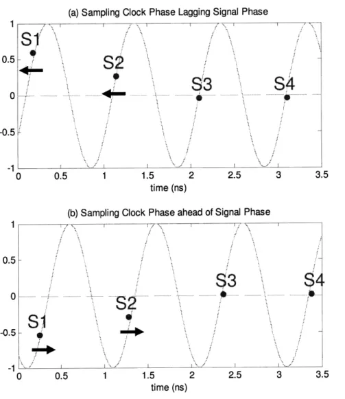
The digital phase tightening algorithm can be best understood by first looking at its end result as shown in Figure 2-1. If the algorithm samples at f samples per second then in the finished state the sampling clock is shifted by 0 from the reference clock to sample the signal at exactly its positive-sloped zero crossings. This shifted phase 0 is exactly the same value as 0.
The algorithm reaches its end goal of sampling at exactly the positive-sloped zero crossings by shifting the phase of the sampling clock based on the sign of each sample. As shown in Figure 2-2, 0 is decreased if the sample is positive and is increased if the sample is negative. Eventually the samples become zero and the algorithm is in lock and stops changing 0.
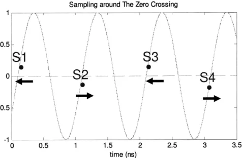
However, only a finite number of steps of a uniform phase shift size can be im-plemented; thus the samples may never become zero. Instead, the algorithm results in 0 alternating between two values that correspond to the smallest possible positive value and the smallest possible negative value for a sample. As shown in Figure 2-3, this becomes the new definition for locking as the average of the two values for 0 is the best estimation for 0. The trade off is that smaller step size results in greater resolution for the estimation and larger step size results in locking in fewer cycles. Since the algorithm stays locked, the initial locking time is not as important as the resolution is. This gives the algorithm its name because the sampling points move toward and tighten around the zero crossings.
By doubling the sampling rate to 2f samples per second, the even samples can lock onto the negative-sloped zero crossings while the odd samples lock onto the positive-sloped zero crossings. Now 0 is shifted twice for each period of Equation
(a) Input Signal f - i N" I / f I J
S 3
....
...
---
--1.5 2 time (ns) (b) Sampling Clock I2.5 3 2.5 3 0.5 1 -0.5 1 time (ns) (c) Reference Clock time (ns)
Figure 2-1: Lock state of digital phase tigtening algorithm with positive edge triggered
sampling (a) Input signal with a phase offset of q from the reference clock (b) Sampling
clock with a phase offset 6 (c) Reference clock
19
si
f"'"r-~--~S2
I I : I i I . \\. AcS4
/ 0.5 -0.5 -0.5 0 -0.5~--~--(a) Sampling Clock Phase Lagging Signal Phase
' i
S2
..
.
i x/su'
3 i iii
i -- i --- ----I / :/ 5 j t \I i ii /SS4
...
.
...
...
...
s
---...--
...
I i r i\.
/
, \,
0 0.5 1 1.5 2 2.5 3 3.5 time (ns)(b) Sampling Clock Phase ahead of Signal Phase
f J t S S
SI
.5.
0 0.5s3
/---S2
ii S f i i i\. 1 1.5 2 2.5 3 3.5 time (ns)Figure 2-2: Shifting the sampling clock to lock onto positive-sloped zero crossings
when (a) 9 the phase offset of the sampling clock is initially greater than q the phase
offset of the signal (b) 0 is initially smaller than
4
20
1 0.5 0 -0.5 -I 0.5V
-0 Si t fi MML I ' ' ' I I -I i I rC iSampling around The Zero Crossing
1
i I I I f I f ; 0.5 -1 S i -0.5 i - *** 0 0.5 1 1.5 2 2.5 3 3.5 time (ns)Figure 2-3: Due to the resolution of the phase shifts, the sampling clock will toggle
around the positive-sloped zero crossings
2.1 instead of only once, thus the locking speed has doubled as shown in Figure 2-4.
However, locking onto both types of zero crossings requires additions to the algorithm,
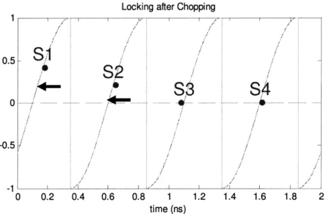
which translates to additional circuitry for implementation. This can be avoided by
inverting Equation 2.1 for every even sample. As shown in Figure 2-5, only
positive-sloped zero crossings exist. This process, called chopping, is easily implemented and
is described in a later section as it also has circuit related benefits.
Lastly, when the sampling rate is doubled again to 4f, the new sets of samples,
between the sets of samples used for locking, automatically fall on the maximum and
the minimum of Equation 2.1. Thus A is determined.
2.1.2
Implementation
One of the main advantages of digital phase tightening is that it is easily implemented with established components as shown in Figure 2-6. The DLL shifts its output, the sampling clock, from its input, the system clock, to lock onto the zero crossings of the ADC's input. Assume the input is of the form Equation 2.1 and f is 1GHz, thus the
Reduced Locking lime /
/
i s iSi
S3
$4
8$5
..
..
...
- --.
--.
..
.
...
...
"t i~iS'
7
----
.---
---S J i St
j
\\/ 0 0.5 1 1.5 2 2.5 3 3.5 time (ns)Figure 2-4: Locking time can be reduced in half when alternating samples are used
to lock onto both positive-sloped and negative-sloped zero crossings
Locking after Chopping
1 1 /
St
+ -E-
S.
1 1.2 1.4 1.6
time (ns)
Figure 2-5: Chopping inverts the input for
all zero crossings to postived-sloped
every other sample, which effectively turns
1 0.5 0 -0.5 -1
Si
* 0.5 0* -0.5 -1S4
0 0.2 0.4 0.6 0.8 1 - - -L~ i ': i r I / )J i i 1 I i. I I I I i ./ADC samples at 4 G samples/s. The digital processing block simply determines the sign of every odd sample. This information guides the DLL to shift the ADC sampling such that the odd samples become locked near the zero crossings. After which, the even samples, falling in between the zero crossing, become the measurements for the amplitude A. Additionally, the front-end of the ADC applies multiplexers to invert the input signal at every other odd sample to simplify the circuitry for digital processing as discussed previously. This technique, called chopping, also reduces the offset noise in ADCs [5].
4GHz
4GHz
DLL
1GHz
ADC
Digital
Processing
Output to CPU
Figure 2-6: System level block diagram for digital phase tightening. The DLL gen-erates a shifted version of the reference clock for the sampling clock of the ADC. The digital processing block determines the direction of the shifts using the ADC's outputs.
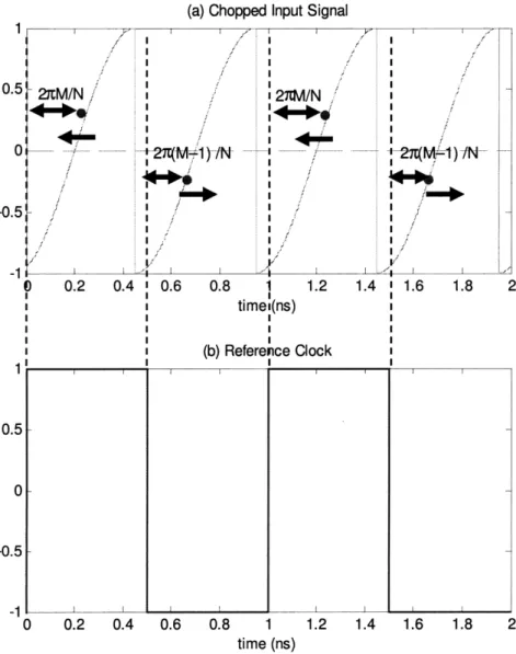
The number of cycles required for the feedback loop to become locked depends on the resolution of the DLL. The DLL can shift its output clock by steps of size 2r/N, where N is the number of delay elements in the delay line. Note that N such shifts completely cover an entire period; thus locking must occur in less than N shifts. The
obtainable resolution for the phase q depends only on N if the ADC has a threshold at zero volts. There exists an integer M that satisfies Equation 2.2.
0 < M. 2 /N -
< 2 /N
(2.2)
When the DLL shifts 0 to M - 27/N then the ADC, regardless of its step size, will sample a positive value and the DLL will shift 0 to (M - 1) • 27/N. For the next phase correction, the ADC will sample a negative value and the DLL will shift 0 back to
M.
2r/N . This process is repeated as illustrated in Figure 2-7. It follows that 5 is in between M - 2r/N and (M - 1) 2/N.On the other hand, the estimation of amplitude A depends on both the ADC resolution and the DLL resolution because it is the quantized value of a sample taken in a range of [-2r/N, 27/N] around 0 + r/2.
2.2
System Overview
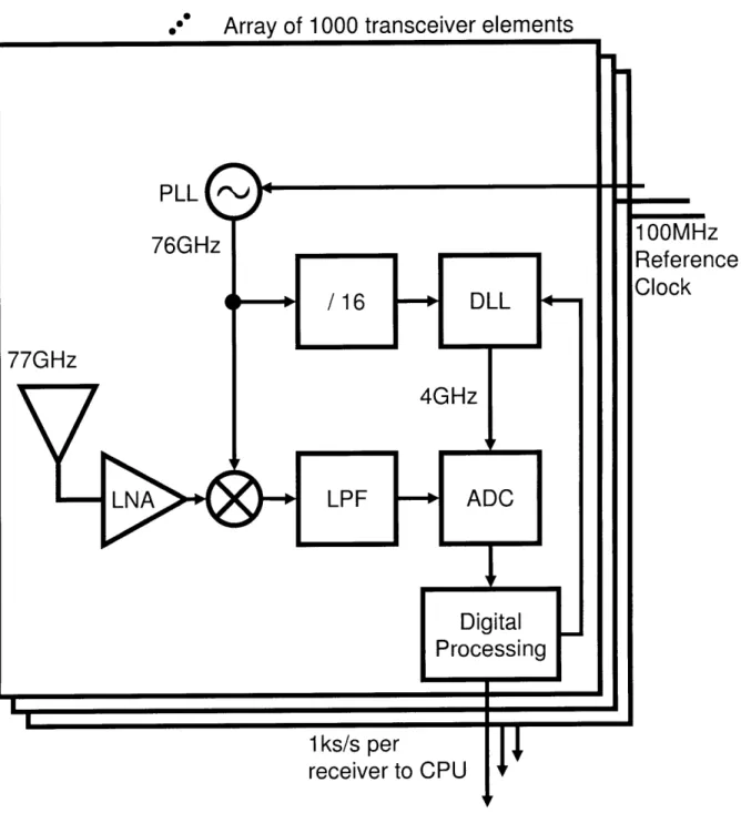
The MMW active imaging system, shown in Figure 2-8, is a planar array of 1,000 elements. Each array element consists of a Per-Antenna Processing (PAP) unit, along with the corresponding antenna for receiving radiation. Each element has a heterodyne architecture with a 76GHz phase lock loop (PLL) and a 1GHz IF. On the transmitter side, a single antenna radiates a 77GHz sinewave. Both the receivers and the transmitter share the same reference clock. Ideally, the signal transmitted and received is a spectrally pure 77GHz tone; however the mismatches in center frequency between the PLLs of the 1000 elements is equivalent to an expansion of the bandwidth of the received signal to 200MHz [1].
The PLL is used to shift the amplified received signal down to IF. A low pass filter (LPF) rejects the high frequency image and other sources of interferences. The result is converted to the digital domain. Using a clock derived by dividing down from the PLL, the analog-to-digital converter (ADC) samples at twice the Nyquist rate, 4Gs/s, to avoid aliasing. Since the antennas use the same reference source as the ADC and the DLL it becomes feasible to assume that their frequencies are in
(a) Chopped Input Signal / I / I ! '2tM/N I 1~ I4 I Si/ I J"k I., 0 0.2 0.4 I 0.6 0.8 1 1.2 1.4 I 1.6 1.8 I I I I time,(ns) (b) Reference CocI I I I I I I I I (b) Reference Clock I I 1 time (ns) 1.2 1.4 1.6 1.8 2
Figure 2-7: The phase offset of the input signal ¢ is in between M - 2r/N and
(M
-
1) - 2ir/N; thus, the sampling clock's phase offset 0 toggles between the two
values. (a) The input signal after chopping with 4 sample points (b) The reference
clock
2atM/N ' i/
i / -0.5 0.5 0 -0.5 -1 0 0.2 0.4 0.6 0.8 1 -11 k-- I IoO°
Array of 1000 transceiver elements
Reference
Figure 2-8: MMW active imaging system. all share a 100MHz reference clock.
lock. By itself, a single received signal represents the superposition of waves reflected towards its antenna from every point in the scene. The central processing unit (CPU) combines the information from each PAP to resolve distinct pixels. A system clock of 100MHz is used to synchronize the CPU and all 1,000 PAPs. Having a low frequency system clock circumvents the high cost of implementing an overly complicated and highly lossy clock distribution system. Furthermore, the data rate from each PAPs to the CPU of lks/s avoids the use of power-hungry circuitry for digital transmission at high data rates across long distances. By reducing the data rate from 4Gs/s to about lks/s in each of the 1000 elements, the digital blocks attempt to reduce the noise using redundancy before sending the data to the CPU. This method of oversampling for noise reduction is described in the next section.
2.3
Averaging for Noise Reduction
The input signal has phase noise D(t) and amplitude noise a(t) is shown in Equation 2.3. All of the noise sources in this chaper are assumed to be white with zero mean.
(1 + a(t)) - A - sin(2rf - t + 0 + 1((t)) (2.3) One of the biggest advantages, following from the simplicity of extracting 0 is the ability to average the phase information to reduce the error in measurement. Similarly, averaging can reduce the amplitude noise of the measurement of A. However, phase noise shifts the sampling off of the peak amplitude, which always results in a measured value smaller than the actual A. Another method is to ignore averaging and use only the maximum and the minimum values to calculate A; this method is most accurate if amplitude noise is assumed to be insignificant. The best approach to measuring A will be determined in future work.
Noise in the system causes erroneous measurements for 0 as shown in Figure 2-9. One noise source of concern is phase noise from the PLL. The current PLL has the following profile for phase noise: -85dBc/Hz at 1MHz offset from 76GHz, -90dBc/Hz at 10MHz offset, and -120dBc/Hz at 100MHz offset. This corresponds to a jitter
of -0.4ps. Assuming the noise source is white, then averaging L samples reduces the standard deviation of the noise by /L. Given the lks/s data rate and the 4Gs/s sampling rate, where half of the samples are used for phase estimation, L is 2,000,000. This averaging reduces the 0.4ps jitter from the PLL into an effective jitter of 280as. However, there are physical limits that prevent the DLL resolution to be lower than 10ps, which introduces a limitation on the accuracy of the phase estimation. The following section will describe this limitation and how it can be resolved.
2.4
Using Noise to Improve Phase Estimation
The finite step size of the DLL introduces deterministic quantization errors. In a signal without noise the quantization error is the distance from q to the nearest DLL step. This is illustrated in Figure 2-10 with the step size normalized to 1. When the DLL is shifting its output by 0, call this state 0, it will detect that its output needs to be delayed to move towards q; thus, in the next cycle the DLL will shift its output by 1, call this state 1. In state 1, the DLL needs to advance its output to move towards 0. In other words, state 0 transitions to state 1 and state 1 transition to state 0 each time with probability 1 as shown in Figure 2-11. Since the DLL is forced to increment
or decrement every cycle, the quantization error alternates between -0 and 1 - q. For any value of b between 0 and 1, the estimated value for 0 will be the average of the DLL steps which is 0.5. If the step sizes are 17.5ps then the worst quantization error is ±8.75ps which occurs when q is very close to 0 or 1.
If the signal has a noise n(t) with a small peak-to-peak value then n(t) has no effect on the phase estimation due to the quantization error. As a result, averaging does not improve the phase estimation when the noise is much smaller than the quantization level. As shown in Figure 2-12, the case with small noise results in the same scenario as Figure 2-11.
If n(t) is uniformly distributed between -0.5 and 0.5 then more than two states will be reached for any value of q. When enough samples are taken, the expectation of the phase estimate equals q. Given the example in Figure 2-13 where q = 0.25,
(a) Chopped Input Signal 1 0.5 0 -0.5 -1 0.5 1 1.5 2 2.5 time (ns)
(a) Input Signal with Noise
1 0.5 0 -0.5 0.5 1 1.5 2 2.5 time (ns)
Figure 2-9: Noise effecting phase and magnitude measurements (a) Ideal input
sam-pled with no noise indicates that the sampling clock's phase offest 0 should not be
changed (b) Noise changes the sample values from the ideal case and indicates 6
should be increased. Furthermore, the amplitude measurement also changed.
Figure 2-10: True value of 0 lies between quantization levels 0 and 1
1
Figure 2-11: When there is no significant amount of noise present, the measured value of 0 alternate between 0 and 1 every cycle
Figure 2-12: Value of 0 with a small noise n(t) lie between quantization levels 0 and 1
I
__
__
3-
the DLL reaches state -1 in addition to 0 and 1. Figure 2-14 illustrates that at state
0 the probabilities of the next state being -1 and 1 are 0.25 and 0.75 respectively.
Since states -1 and 1 always transition to state 0, half of the DLL steps are at 0.
Fur-thermore, state 1 is expected to be reached three times more than state -1. Equation
2.4 shows that the expectation of the phase estimate equals 0 as quantization error
has been reduced to zero. When the peak-to-peak value of the uniformly distributed
noise is not 1 or another positive integer, the quantization error will not be completely
eleminiated [6].
-Figure 2-13: Value
and 1
.125 -1 +.50
0 +.375
1= .25
-.
25
.25
.75
of ¢ with a larger noise n(t) lie between quantization levels -1, 0,
.25
.75
Figure 2-14: With an increased noise, the measured value of ¢ switches between -1,
0, and 1 randomly
The total noise contribution from the input signal, the ADC, and the DLL is
(2.4)
-1
usually enough to correct the quantization error [7]. A process called dithering can be applied to intentionally add more noise to ensure that quantization errors are reduced. The noise in a real system has a Gaussian distribution. When the root mean square (rms) jitter of a Gaussian noise source is 0.5 steps or greater, quantization error is essentially eliminated and the system noise can be reduced by averaging [7]. Figure 2-15 shows the calculated quantization error for values of 0 between 0 and 1 when the system has a Gaussian noise source with a rms jitter of 0.5 steps or 8.75ps. Figure 2-16 shows the quantization errors when the rms jitter is 0.35 and 0.45 steps for comparison. The quantization error decreases exponentially when the rms jitter changes from 0.35 to 0.5 steps. By averaging 2,000,000 samples of a signal with 8.75ps rms jitter, the phase estimation will have a jitter of 6.2fs and a quantization error determined by Figure 2-15. Note that the uncertainty of the phase estimation, represented by the jitter, is significantly larger than the deterministic offset, which is equivalent to the quantization error.
Quantization Error VS Phi (RMS = 0.5)
1.4 1.2 0 8 0.8 .N 0.6
4'-O
0.4 0.2 0 0 0.2 0.4 0.6 0.8 1 Phi (step)Figure 2-15: Calculated quantization error of the phase estimations for values of q between 0 and 1 with a Gaussian noise source with rms jitter of 0.5 steps
(a) Quantization Error VS Phi (RMS = 0.35)
0.2 0.4 0.6
Phi (step)
(b) Quantization Error VS Phi (RMS = 0.45)
0.2 0.4 0.6 0.8 1
Phi (step)
Figure 2-16: Quantization error of the phase estimations for values of 5 between 0 and 1 when the Gaussian noise source has a rms jitter of (a) 0.35 steps (b) 0.45 steps
300
200
Chapter 3
Proof of Concept Integrated
Circuit for Phase Tightening
The system incorporates enough abstractions to allow the key blocks to be designed and analyzed separately. The DLL, the ADC, and the digital processing block are designed and implemented for a proof-of-concept system, as shown in Figure 3-1. Due to constraints placed by the technology, the input signal to the DLL is reduced to 2.4GHz and the input signal to the comparator is reduced to 0.6GHz. The clock is derived by dividing the output from the 76GHz PLL; however, a signal generator will be used to produce the 2.4GHz signal. Furthermore, the ADC is replaced by a 1-bit comparator that samples at 1.2Gs/s. Sampling at the Nyquist frequency, the system, using the method described in the previous section, is able to find the zero crossings to determine the phase information.
3.1
DLL Operation And Architecture
A close cousin of the PLL, the DLL consists of three main blocks: the delay line, the phase detector (PD) and the low pass filter (LPF) as shown in Figure 3-2. Normally, the DLL is used to buffer the incoming clock signal; thus, giving only one output. The DLL operates by passing the input signal through a delay line and comparing its output to the input signal. The PD and LPF extracts this error signal to control the
Reference
Clk
Input Signal
@ 0.6GHz
ADC/
[
Digital
Comparator
Processing
5-Bit Output to Logic Analyzer
@1.2GHz
Figure 3-1: Block diagram of the implemented system on chip. External 2.4GHz signal is used for the reference clcok and external 0.6GHz signal is used as the comparater's input. The system outputs 5 bits at 1.2GHz
delay through the delay line. The standard architecture can be modified for other applications.
Clk in
PD
LPF
Clk
_out
S Delay Line
-Figure 3-2: Traditional DLL architecture with phase detector, low pass filter, and delay line
Our application requires selecting from multiple phases; thus an architecture al-lowing multiple outputs is required. The modified architecture shown in Figure 3-3 is implemented [8]. The core DLL is almost identical to the canonical DLL shown in Figure 3-2; however, the delay line outputs shifted versions of the input at 24 different phases. Each phase is 7r/12 radians or 17.5ps from the next one. The multiplexer then passes a selected phase to the frequency divider, which buffers the output signals and sets its duty cycle to fifty percent [9].
The delay line divides the 420ps long period of a 2.4GHz input signal into 24 equal sized steps of 17.5ps, where each step is selected by a unique digital code of the DLL. However, the DLL output has a 840ps long period and a 1.2GHz frequency; 24 steps of 17.5ps each cannot cover the entire 840ps period. Therefore each digital code corresponds to two delay steps that are 7r radians apart at 1.2GHz. However, the delay steps progress incrementally and wraps around; thus, combining the history of the digital codes with the current digital code uniquely determining the delay step.
CIk in
r
-- -- n-2.4 GHzICore
DLL
#r
24
I
MuxI
CIk
out
S
1 2GHz
Frequency Divider
I
-Figure 3-3: Modified DLL architecture using a multiplexer to select different phase offsets from the reference signal and a frequency detector to generate 50% duty cycle at the output
3.1.1
Delay Element And Delay Line
The delay elements are four current starved inverters; the pseudo-differential configu-ration is as shown in Figure 3-4 and the detailed transistor level schematic is show in Figure 3-5 [4]. The control voltage sets the maximum amount of current allowed in the NMOS transistor. Current ID is related to propagation delay tdelay by Equation
3.1 [10]. Equation 3.1 models the propagation delay as the time it takes ID to charge or discharge a load capacitor C to a fixed voltage VDD/ 2.
tdelay = CVDD (3.1) ID
Since only the pull down current is affected, there is asymmetry between the rise time and the fall time. Asymmetry causes skew between the positive and negative terminals, which results in unpredictability for the propagation time. Tying both outputs to each other through a pair of secondary inverters reduces this problem. Figure 3-6 shows that passing a signal with an initial skew through two delay elements significantly reduces the skew at the output [11]. A smaller ratio between the size of the primary inverter pair and the size of the secondary pair can correct more skew;
IN+
IN-Figure 3-4: Schematic view of delay element with for positive feedback
OUT-OUT+
cross coupled inverters at the output
Figure 3-5: Transistor view of delay element
however, a larger secondary pair presents more loading and slows the propagation time. A ratio of four to one is chosen to allow for a fastest propagation time, when the control signal is at VDD, of 16.5ps. This is only slightly slower than 12.5ps, which is the propagation delay of the unit size inverter. The input signal has a swing of
VDD, 60ps rise and fall times, and variable skew.
A chain of two delay elements can also be used to buffer weak clock signals. Figure 3-7 shows the rise and fall times at the output when the input signal has a varying rise and fall time. Figure 3-8 shows the amplitude at the output when the input signal has a varying amplitude.
Output Skew VS Input Skew 30 25 & 20 S15-0 1S15-0 5-0 10 20 30 40 50 60 Input Skew (ps)
Figure 3-6: The amount of skew reduction by the delay element at its output when the differential input is skewed
the signal should be identical through each delay element of the delay line. The delay line, as in Figure 3-9, is a chain of N delay elements. When the DLL is in lock, the output of the last delay element should have the same phase as the input to the DLL and the resolution is of the form Equation 3.2. Also, the phase offset after the xth delay element is x - 2i/N radians or x - 420/N ps for 2.4GHz.
period
tdelay = (3.2)
The delay line is the main source of noise in the DLL. The total noise contribution from the delay line scales linearly with the number of delay stages [12]. Equation 3.3 is used to estimate the noise generated by the delay line [13]. On the other hand, the resolution of the delay line is inversely proportional to the number of delay elements. The incremental increases in noise eventually outweigh the improvements in resolution. Using 24 stages, the delay line has a resolution of 17.5 ps and contributes
Output Rise And Fall Times 27 26 25 24 - -23 " 22- - - Rise Time 4- Fall Time 21 -20 19 18 17 I 0 20 40 60 80 100
Input rise and fall times (ps)
Figure 3-7: The effect of the edge transition rate of the input on the rise and fall times of the output after buffering by the delay element
2kTyroC
tjitter,total = N titter,stage N. - (3.3)
cLPCox(VDD - VT)2
There are additional limits on the resolution of the DLL. Equation 3.2 shows the resolution cannot be smaller than the smallest possible tdelay. However, there is a technique, phase interpolation, that allows for the averaging of the phases from the delay lines [14]. Unfortunately, the phase is determined by combining the currents from different delay elements, which produces high noise and non-linearity.
Furthermore, 24 can be factored as in 24 = 2 - 3 - 4. This allows for the imple-mentation of a cascade of a 2:1, 3:1, and 4:1 multiplexers with buffers in between. A chain of multiplexers is much more robust than a N: 1 multiplexer.
Lastly, Figure 3-10 shows the delay of each delay element and the locking frequency for the DLL as a function of the control voltage. The DLL is flexible enough to work in the range of frequencies between 400MHz and 2.5GHz. However, note that with decreasing frequency the charge pump (CP) pumps current over a longer time during each cycle, which results in greater control voltage changes and greater frequency
Output Amplitude VS Input Amplitude 0.6 0.5 0.4 0.3 0.2 10-1 100
Differential input amplitude (Volts)
Figure 3-8: The effect of the amplitude of the input on the ouput swing after buffering by the delay element
1-3600 2-3600
Figure 3-9: Delay line: a chain of identical delay elements
changes. Eventually, the frequency changes so greatly that the DLL overshoots the phase correction and falls out of lock; thus, the DLL cannot be slowed down to operate at any arbitrary low frequency.
3.1.2
Phase Detector, Charge Pump And Low Pass Filter
The PD, CP, and LPF comprise the feedback control portion of the DLL. In a simple DLL, an exclusive-or (XOR) gate is used to compare the delay line output to the input signal. When the XOR gate is used to compare two signals, the smallest delay difference it can resolve is larger than the gate's propagation delay [15]. The fastest
(a) Delay VS Control Voltage
0.4 0.6 0.8 1 1.2 1.4 1.6 Delay line control voltage (Volts)
(b) Frequency VS Control Voltage
0.4 0.6 0.8 1 1.2
Delay line control voltage (Volts)
1.4 1.6
Figure 3-10: voltage
(a) Propagation delay of single delay element with changing control
(b) Resulting frequency of delay line due to changes in the control voltage of the delay elements
combinational gate, the inverter, has a propagation delay or 12.5ps; thus the XOR gate, significantly slower than the inverter, cannot resolve delay differences that are close to the step size of the DLL.
10 4 -103 102 10-0.2 3-N 2.5 = 2 S1.5 c - 0.5 U- 0 0.2
A faster phase detector can be constructed using source-coupled logic (SCL). A latch constructed using SCL, shown in Figure 3-11, can detect a small phase dif-ference because it is differential and uses current switching instead of relying on a voltage signal [16]. When the CLK signal is high, the circuit functions as an ordinary differential amplifier with the output value changing with the input. When CLK_bar is high, the circuit is in the hold stage. The two cross coupled NMOS transistor are in positive feedback and hold the output value constant. These phase detectors can detect phase differences as small as 4ps, which is more than three times smaller than the resolution of the XOR gate.
Vdd
Vbias
Q
Qbar
D_bar
D
CIk
Clk bar
Figure 3-11: SCL latchThe ideal function of the PD is described as follows. Two latches are constructed, one for the UP signal and one for the DOWN signal. When the DLL input is con-nected to CLK and CLK_bar of the latch and the last delay element's output Vl,,st is connected to the differential input of the latch, D and D_bar, a faster Vlat generates a voltage high for DOWN. DOWN remains high until the next positive edge of the DLL input. And when DOWN is high, the CP decreases the voltage feeding the LPF, which increases the propagation delay of each delay element and the total propagation
delay of the delay line. Eventually, the delay line is slowed so that Viast matches the input to the DLL. However, when the input signal is leading then the latch remains unresponsive. The latch generating the UP signal is analogous with the exception that the complimentary output of the latch is used as UP. When the phase difference becomes too small to be detected by the phase detectors, the DLL enters the tristate stage where the delay between Vast and the input remains constant. This is usually in the neighborhood of 3 to 4ps.
The outputs of the SCL latches drive the input of a single-ended charge pump. Although differential charge pumps have the advantages of low switch mismatch, higher output voltage range, and better immunity to supply and substrate noise, the single-ended topology is chosen because, in addition to having a lower power consumption during tri-state operation, it does not require an additional loop filter and common mode feedback circuitry [17]. Furthermore, mismatch between the pull-up PMOS and the pull-down NMOS has minimized effect to this situation because the rate of frequency change over one output cycle is low such that any given cycle will not have a significant impact on the output frequency of the DLL.
Figure 3-12 shows the topology of the chosen charge pump design. Transistors M1 and M6 are for active control of the charge pump. The switches are placed at the source to force both devices to always be in saturation, which allows better matching. Additionally, this topology switches faster because each input drives only a single transistor so that there is lower parasitic capacitance.
When both of these devices are off, the CP enters tri-state operation where power is saved because there is no dynamic current flowing from supply. However, there is a maximum leakage current of 400nA present through transistors M1 and M6. The voltage value changes by only one to two mili-volts during a cycle when the CP is active and driving 8,/A; therefore, the leakage current has a trivial effect on the output voltage.
Transistors M2 through M5 are a part of the current mirror network which is cas-caded to increase the output impedance so that the current variation is less sensitive to the output voltage. Lastly, C1 and C2 are added to reduce the charge coupling to
UP
M
M1C1
M2
M3
bias1
Out
M4
[
bias2
M5
DOWN-
M6
Figure 3-12: Charge pump
the gate and to help enhance the switching speed.
In addition to the CP, an off-chip signal RST can also affect the control voltage for the delay line. RST is used to initialize the control voltage at VDD such that the bottom transistor in each delay element is in strong inversion at the start of operations. RST achieves this by driving a large pull-up PMOS transistor into strong inversion. Once RST is released, the CP and the rest of the system will adjust to lock onto the input signal. Simulations show that locking occurs in less than 200 clock cycles or 100ns as shown in Figure 3-13. Furthermore, due to the sensitivity of the PD and the level of the leakage current in tri state, the DLL remains in lock
indefinitely. However, when it falls out of lock, it will return to the locked state in fewer clock cycles than the initial locking time.
Transient
Response
1.210
-1.190
1.170 S1.150150-1.110
0.00
20.0n
40.0n
60,0n80,0n
100n
time ( s )Figure 3-13: After the RST signal is released at 10ns, the control voltage of the DLL settles within 10% of its final value after 40ns
A second order LPF, shown in 3-14, integrates the output of the CP and converts it to the control voltage for the delay line. The loop filter is a complex impedance in parallel with the input capacitance of the delay line; however, C1 and C2 are sized 500fF and 100fF respectively such that they dominate the capacitance seen at this node. The total gate capacitance from the transistors on the delay line is 150fF. Furthermore, C1 and C2's sizing also mitigate the affect of leakage current; thus, reducing the risk of the DLL drifting out of lock. The disadvantage of higher capacitance is that it increases the time required for locking. As stated earlier, this is not essential as the DLL only needs to lock once. The shunt capacitor C1 is placed to remove discrete voltage steps at the control voltage of the delay line due to instantaneous changes in the CP current output.
3.1.3
Frequency Divider for Duty Cycle Correction
As stated earlier, the primary use of the DLL is to generate a buffered clock signal with a 50 percent duty cycle. Due to the changing rise and fall times of the delay
C1
R2
C2
Figure 3-14: Low Pass Filter
elements, the output of the delay line can stray far from a 50 percent duty cycle. The conventional DLL uses a duty cycle correction (DCC) circuit to address this problem. The DCC circuit works by comparing points on the rising edge of the output against a threshold value via an amplifier. However, a signal with a rise time smaller than 20ps is too fast to be adjusted by a typical DCC circuit.
Taking advantage of a higher frequency reference source divided down from the 76GHz PLL, a frequency divider replaces the conventional DCC circuit. The delay line drives the frequency divider directly and every positive edge from the delay line cause the frequency divider's output to toggle. Thus, the frequency divider's output will remain high for one period of the delay line's output and remain low for one period of the delay line's output also. Since the delay line's output is periodic, this guarantees that the frequency divider outputs a signal with a 50 percent duty cycle. This system varies from the conventional DLL in that the frequency of the final output is half the frequency of the input instead of being equal to it.
The schematic of the frequency divider is shown in Figure 3-15. It is two latches tied together in the standard configuration. SCL latches, identical to the ones used for phase detection, are used because a static CMOS divider cannot operate at 2.4GHz [18]. One disadvantage of the SCL divider is that the circuit has static current. While
Q
bar
Clk
Clkbar
Figure 3-15: Frequency divider
operating at 2.4GHz, the SCL divider consumes 7.48mW. Figure 3-16 demonstrates the effectiveness of the divider at fixing the duty cycle. Lastly, the divider adds flexibility to the system as it can operate with an input in the frequency range of 10MHz to 20GHz.
3.2
Comparator
A regenerative latch, as shown in Figure 3-17, is used as the comparator to measure the input signal. Often, a preamplifier with low gain, 2 to 4, accompanies the com-parator. However, at higher frequencies, the preamplifier rarely has gain above unity, but it is necessary to remove the "kickback." "Kickback"' is when the turning on and off of transistors in the latch affect the input voltage to the latch [19]. We have opted to remove the preamplifier stage because it slows down the comparator and simulations show that kickback is insignificant. When EN is high, the latch functions as a differential amplifier with positive feedback at the output. Transistors M3 and M5 amplify the small input differential voltage. Transistors M1 through M4 amplifies the differential signal at nodes X and Y by pulling the small analog value to a digital
![Figure 1-1: Image formation for conventional digital camera using a lens to focus [1]](https://thumb-eu.123doks.com/thumbv2/123doknet/14746702.578429/12.918.180.787.408.871/figure-image-formation-conventional-digital-camera-using-focus.webp)
![Figure 1-2: Incident wave received by a two element array for beamforming [1]](https://thumb-eu.123doks.com/thumbv2/123doknet/14746702.578429/13.918.187.674.428.663/figure-incident-wave-received-element-array-beamforming.webp)