DOCTORAT DE L'UNIVERSITÉ DE TOULOUSE
Délivré par :
Institut National Polytechnique de Toulouse (INP Toulouse) Discipline ou spécialité :
Micro Nano Systèmes
Présentée et soutenue par :
Mme LAVINIA-ELENA CIOTIRCA le mardi 23 mai 2017
Titre :
Unité de recherche : Ecole doctorale :
System design of a low-power three-axis underdamped MEMS
accelerometer with simultaneous electrostatic damping control
Génie Electrique, Electronique, Télécommunications (GEET)
Laboratoire d'Analyse et d'Architecture des Systèmes (L.A.A.S.) Directeur(s) de Thèse :
MME HELENE TAP
Rapporteurs :
M. JEROME JUILLARD, SUPELEC
M. PASCAL NOUET, UNIVERSITE MONTPELLIER 2
Membre(s) du jury :
M. PHILIPPE BENECH, INP DE GRENOBLE, Président Mme HELENE TAP, INP TOULOUSE, Membre M. OLIVIER BERNAL, INP TOULOUSE, Membre
The research work presented in this thesis was carried out between 2014 and 2017 at the Laboratory for Analysis and Architecture of Systems (LAAS) in Toulouse with collaboration of the Sensors Solutions Design (SSD) Team at NXP Semiconductors (previously Freescale Semiconductors).
Firstly, I would like to express my sincere gratitude to Prof. Hélène Tap and Mr. Philippe Lance for offering me the opportunity to carry out this research and for supervising this project. I would like to thank Hélène for her continuous support and guidance and for always being positive towards my work. Her motivation and patience helped me in all the time of research and writing of this thesis. I would also like to thank Philippe for his constant support and for the worthy advice on both research as well as on my career development.
Further, I would also like to thank the rest of my thesis committee Prof. Pascal Nouet, Prof. Jérôme Juillard and Prof. Philippe Benech for taking the time to review this thesis and for their insightful comments.
This thesis would not have been possible without the close guidance of Dr. Olivier Bernal, Mr. Jérôme Enjalbert and Mr. Thierry Cassagnes. I would like to express my gratitude for all their help, technical expertise and constant encouragement. I will always appreciate and remember their patience and kindness.
I am grateful to Dr. Robert Dean and Dr. Chong Li for offering me the opportunity to develop this research work within their facilities during my stay at Auburn University, USA.
I would also like to thank Ms. Peggy Kniffin, Mr. Aaron Geisberger and Mr. Bob Steimle for the MEMS modeling guidance and Mr. Clément Tronche, Mr. Francis Jayat and Mr. Philippe Calmettes for providing their help with the experimental set up and my samples demands.
Likewise, I want to hereby acknowledge the contributions of my colleagues at NXP Semiconductors as well as all the OSE (LAAS) group members. In particular, my sincere thanks go to all the doctoral students I had the chance to meet during this research work, for all their help and day to day support: Antonio Luna Arriaga, Evelio Ramirez Miquet, Jalal Al Roumy, Laura Le Barbier, Mohanad Albughdadi, Raül da Costa Moreira, Lucas Perbet, Blaise Mulliez, Yu Zhao, Fernando Urgiles, Harris Apriyanto and Mengkoung Veng.
I have no words to express my gratitude to all the friends I had or have made during these last three years. Their permanent encouragement, motivation, attention and care helped me to successfully complete this work. I would like to thank all of them for the special moments we have shared together and for never letting me down. Infinite thanks!
Last but not the least, I would like to present my deepest gratitude to my parents, Mia and Mircea, who have always encouraged and supported me to follow my dreams! I would like to thank them, and my little brother, Liviu, for the unconditioned love, trust, kindness and for being a constant source of inspiration. To them I dedicate this thesis!
Recently, consumer electronics industry has known a spectacular growth that would have not been possible without pushing the integration barrier further and further. Micro Electro Mechanical Systems (MEMS) inertial sensors (e.g. accelerometers, gyroscopes) provide high performance, low power, low die cost solutions and are, nowadays, embedded in most consumer applications.
In addition, the sensors fusion has become a new trend and combo sensors are gaining growing popularity since the co-integration of a three-axis MEMS accelerometer and a three-axis MEMS gyroscope provides complete navigation information. The resulting device is an Inertial measurement unit (IMU) able to sense multiple Degrees of Freedom (DoF).
Nevertheless, the performances of the accelerometers and the gyroscopes are conditioned by the MEMS cavity pressure: the accelerometer is usually a damped system functioning under an atmospheric pressure while the gyroscope is a highly resonant system. Thus, to conceive a combo sensor, a unique low cavity pressure is required. The integration of both transducers within the same low pressure cavity necessitates a method to control and reduce the ringing phenomena by increasing the damping factor of the MEMS accelerometer. Consequently, the aim of the thesis is the design of an analog front-end interface able to sense and control an underdamped three-axis MEMS accelerometer.
This work proposes a novel closed-loop accelerometer interface achieving low power consumption. The design challenge consists in finding a trade-off between the sampling frequency, the settling time and the circuit complexity since the sensor excitation plates are multiplexed between the measurement and the damping phases. In this context, a patented damping sequence (simultaneous damping) has been conceived to improve the damping efficiency over the state of the art approach performances (successive damping).
To investigate the feasibility of the novel electrostatic damping control architecture, several mathematical models have been developed and the settling time method is used to assess the damping efficiency. Moreover, a new method that uses the multirate signal processing theory and allows the system stability study has been developed. This very method is used to conclude on the loop stability for a certain sampling frequency and loop gain value.
Next, a CMOS implementation of the entire accelerometer signal chain is designed. The functioning has been validated and the block may be further integrated within an ASIC. Finally, a discrete components system is designed to experimentally validate the simultaneous damping approach.
L’intégration de plusieurs capteurs inertiels au sein d’un même dispositif de type MEMS afin de pouvoir estimer plusieurs degrés de liberté devient un enjeu important pour le marché de l’électronique grand public à cause de l’augmentation et de la popularité croissante des applications embarquées.
Aujourd’hui, les efforts d'intégration se concentrent autour de la réduction de la taille, du coût et de la puissance consommée. Dans ce contexte, la co-intégration d’un accéléromètre trois-axes avec un gyromètre trois-trois-axes est cohérente avec la quête conjointe de ces trois objectifs. Toutefois, cette co-intégration doit s’opérer dans une même cavité basse pression afin de préserver un facteur de qualité élevé nécessaire au bon fonctionnement du gyromètre. Dans cette optique, un nouveau système de contrôle, qui utilise le principe de l’amortissement électrostatique, a été conçu pour permettre l’utilisation d’un accéléromètre sous-amorti naturellement. Le principe utilisé pour contrôler l’accéléromètre est d’appliquer dans la contre-réaction une force électrostatique générée à partir de l’estimation de la vitesse du MEMS. Cette technique permet d’augmenter le facteur d’amortissement et de diminuer le temps d’établissement de l’accéléromètre.
L’architecture proposée met en œuvre une méthode novatrice pour détecter et contrôler le mouvement d’un accéléromètre capacitif en technologie MEMS selon trois degrés de liberté : x, y et z. L'accélération externe appliquée au capteur peut être lue en utilisant la variation de capacité qui apparaît lorsque la masse se déplace. Lors de la phase de mesure, quand une tension est appliquée sur les électrodes du MEMS, une variation de charge est appliquée à l’entrée de l’amplificateur de charge (Charge-to-Voltage : C2V). La particularité de cette architecture est que le C2V est partagé entre les trois axes, ce qui permet une réduction de surface et de puissance consommée. Cependant, étant donné que le circuit ainsi que l’électrode mobile (commune aux trois axes du MEMS) sont partagés, on ne peut mesurer qu’un seul axe à la fois.
Ainsi, pendant la phase d'amortissement, une tension de commande, calculée pendant les phases de mesure précédentes, est appliquée sur les électrodes d'excitation du MEMS. Cette tension de commande représente la différence entre deux échantillons successifs de la tension de sortie du C2V et elle est mémorisée et appliquée trois fois sur les électrodes d’excitation pendant la même période d’échantillonnage.
Afin d’étudier la faisabilité de cette technique, des modèles mathématiques, Matlab-Simulink et VerilogA ont été développés. Le principe de fonctionnement basé sur l’amortissement électrostatique simultané a été validé grâce à ces modèles. Deux approches consécutives ont été considérées pour valider expérimentalement cette nouvelle technique : dans un premier temps l’implémentation du circuit en éléments discrets associé à un accéléromètre sous vide est présentée. En perspective, un accéléromètre sera intégré dans la même cavité qu’un gyromètre, les capteurs étant instrumentés à l’aide de circuits CMOS intégrés. Dans cette cadre, la conception en technologie CMOS 0.18µm de l’interface analogique d’amortissement est présentée et validée par simulation dans le manuscrit.
i Contents ... i List of Figures ... v List of Tables ... ix List of Abbreviations ... xi
Introduction
... 1A. Background and motivation ... 1
B. Research direction and contributions ... 1
C. Thesis organization ... 2
1. Inertial sensors
... 51.1 Introduction ... 5
1.2 Degrees of freedom and types of motion in inertial sensors ... 5
1.3 Consumer market MEMS inertial sensors ... 6
1.4 Discrete inertial sensors ... 8
1.4.1 Accelerometers ...9
A. Piezoresistive acceleration sensing ...9
B. Piezoelectric acceleration sensing ...10
C. Capacitive acceleration sensing ...10
D. Other acceleration sensing methods ...12
1.4.2 Gyroscopes ...13
1.5 Combo Sensors ... 14
1.6 Summary ... 16
2. CMOS MEMS Accelerometers
... 172.1 Mechanical capacitive sensing element and second order mass spring damper model ... 17
ii
2.3 Electrostatic actuation ... 21
2.3.1 Electrostatic Actuation mechanism ...21
2.3.2 Static Pull-in voltage ...22
2.3.3 Spring Softening Effect...23
2.4 CMOS Capacitive Accelerometers Interfaces ... 24
2.4.1 Open-loop capacitive architectures for MEMS accelerometers ...25
2.4.2 Closed-loop capacitive architectures for MEMS accelerometers ...27
2.5 Summary ... 30
3. Three-axis high-Q MEMS accelerometer with electrostatic damping
control – modelling
... 333.1 Introduction ... 33
3.2 Three-axis Sensor Element ... 34
3.2.1 Sensor Design ...34
3.2.2 Matlab-Simulink model and s-domain transfer function ...36
3.2.3 z-domain MEMS transfer function ...39
3.3 Analog interface: Charge-to-voltage amplifier modeling ... 41
3.4 Voltage to force conversion ... 43
3.4.1 Electrostatic damping linearity principle ...43
3.4.2 Linearity of the voltage-to-force conversion ...45
3.4.3 Bias calculation for electrostatic force optimization ...47
3.5 Discrete Controller: Derivative Block ... 49
3.5.1 Derivative block – principle of operation ...49
3.5.2 Derivative block - modeling ...51
3.6 Damping approaches ... 52
3.4.1 Successive damping ...53
3.4.2 Simultaneous damping ...56
3.4.3 Performances and choice of architecture ...57
3.7 Multirate controller modeling in z-domain ... 59
iii
3.9 Summary ... 64
4. Towards a CMOS interface for a three-axis high Q MEMS
accelerometer with simultaneous damping control
... 654.1 System design of a low-power three-axis underdamped MEMS accelerometer with simultaneous electrostatic damping control ... 65
4.2 MEMS Accelerometer Verilog A – Spectre Model ... 66
4.3 Charge to voltage converter (C2V) ... 69
4.3.1 Block diagram and clock diagram ...69
4.3.2 Basics of CMOS Analog Design and C2V Architecture choice ...71
4.3.3 Design and performances ...74
4.4 Switched capacitor derivative block ... 77
4.5 Derivative gain amplifier ... 82
4.6 CMOS Switches ... 88
4.7 Excitation signals block ... 90
4.8 Closed-loop system validation ... 91
4.9 Summary ... 92
Conclusions and perspectives... 95
Bibliography ... 97
v
Figure 1.1 A representation of the possible movements of an object in a three-dimensional space
[Snyder, 2016] ...6
Figure 1.2 MEMS revenue forecast 2015-2021 per application [Yole, 2016] ...6
Figure 1.3 (a) Accelerometer applications vs. performances [Domingues, 2013] ...7
Figure 1.3 (b) Gyroscope applications vs. performances [Domingues, 2013] ...7
Figure 1.4 An illustration of a piezoresistive accelerometer ...9
Figure 1.5 An illustration of a piezoelectric accelerometer ...10
Figure 1.6 An illustration of a capacitive accelerometer with interdigitated fingers ...11
Figure 1.7 Typical structure of in-plane (left) and out-of-plane (right) capacitive MEMS accelerometer [Renaut, 2013] ...12
Figure 1.8 Functioning principle of in-plane (left) and out-of-plane capacitive MEMS accelerometer [Renaut, 2013] ...12
Figure 1. 9 A representation of the Coriolis gyroscope model ...13
Figure 1.10 Inertial sensors revenue forecast 2012-2019 [Yole, 2014] ...14
Figure 1.11 A plot of the Quality factor (Q) vs. MEMS cavity pressure (left) and the frequency response of a second order mass spring damper system (right)...15
Figure 2.1 An illustration of a second order mass spring damper system ...17
Figure 2.2 An illustration of the capacitive sensing principle ...19
Figure 2.3 Capacitance variation dependency on MEMS displacement and the linear region of operation (highlighted in red) ...20
Figure 2.4 An illustration of a single electrode motion structure ...22
Figure 2.5. An illustration of a three-plate capacitive structure ...24
Figure 2.6 Conceptual block diagram of a closed-loop MEMS accelerometer ...25
Figure 2.7 Block diagram of the open-loop digital Σ∆ interface [Amini, 2004] ...26
Figure 2.8 Block diagram of an nth order Σ∆ digital closed-loop accelerometer ...28
Figure 2.9 Block diagram of an analogue closed-loop accelerometer ...30
Figure 3.1. Three-axis closed-loop underdamped MEMS accelerometer with electrostatic damping control ...34
vi
Figure 3.2. An illustration of the dual-mass three-axis differential accelerometer with self-test
capabilities and the analog frond end block diagram ...35
Figure 3.3 An illustration of the Simulink model for the open loop MEMS accelerometer ...37
Figure 3.4. MEMS accelerometer response in open loop configuration to a 1g step acceleration for different quality factors: (a) Q=1, (b) Q=50 and (c) Q=2000 ...38
Figure 3.5 Step response of the open loop accelerometer for Q=5 ...39
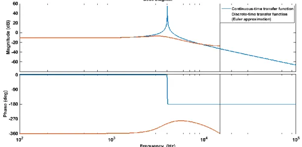
Figure 3.6 Bode plot of the continuous-time MEMS transfer function (blue) and the associated discrete-time Euler approximated TF (red) for fs=30kHz and Q=2000 ...40
Figure 3.7 Bode plot of the continuous-time MEMS transfer function (blue) and the associated discrete-time Tustin approximated TF (red) for fs=30kHz and Q=2000 ...41
Figure 3.8 Block diagram of the capacitive sensing element and the AFE’s first stage with its chronograms ...42
Figure 3.9 An illustration of the MEMS and the C2V simplified models ...42
Figure 3.10 An illustration of a parallel plate capacitive sensor and the electrostatic forces applied on the proof mass ...43
Figure 3.11 Net electrostatic force simulation when the input acceleration varies from -8g to 8g and the control voltage Vctrl varies from -0.4V to 0.4V ...46
Figure 3.12 Net electrostatic force nonlinearity when the input acceleration varies from -8g to 8g and the control voltage Vctrl varies from -0.4V to 0.4V ...46
Figure 3.13 Excitation signals simulations using the optimal values found for VB and Vctrl...48
Figure 3.14 Net electrostatic forces simulation when VB varies from 0V to 0.8V ...49
Figure 3.15 System block diagram ...50
Figure 3.16 Derivative simulation for several sampling rates (a) Ts=2µs (b) Ts=5µs and (c) Ts=10µs (discrete derivative – green and continuous-time derivative red waveform) ...50
Figure 3.17 Block diagram of the derivative model where S&H refers to sample and hold ...51
Figure 3.18 Simulation results of the derivative block ...52
Figure 3.19 Classical approach: successive damping chronograms ...53
Figure 3.20 (a) Block diagram model of the successive damping system ...54
Figure 3.20 (b) Sensor model used in Figure 3.20 (a) to output the charge variation due to the acceleration variation ...54
Figure 3.20 (c) Derivative model used in Figure 3.20 (a) to output the control voltage V_ctrlx ..55
Figure 3.21 Clock chronograms used to control the closed loop system implementing successive damping ...55
vii
Figure 3.23 Clock chronograms used to control the closed loop system implementing
simultaneous damping ...57
Figure 3.24 Electrostatic force waveforms for both approaches: successive and simultaneous damping ...58
Figure 3.25 Settling time simulation results for both approaches: successive and simultaneous damping ...58
Figure 3.26 Simplified block diagram of the discretized system ...59
Figure 3.27 Simplified discrete model using up-sampling and down-sampling blocks ...60
Figure 3.28 Simplified Discrete model for the multirate controller ...61
Figure 3.29 Equivalent open loop system ...63
Figure 3.30. (kd, Ts) stable points ...63
Figure 4.1. Block diagram of the accelerometer signal chain for x-axis ...66
Figure 4.2. An illustration of the MEMS accelerometer Cadence symbol ...67
Figure 4.3 Open-loop MEMS displacement for Q=2 and Q=2000 ...68
Figure 4.4 Open-loop plates configuration for electrostatic force test ...68
Figure 4.5 (a) Block diagram of the AFE’s first stage (C2V) ...70
Figure 4.5 (b) Chronograms of the C2V block and x-axis excitation signals...70
Figure 4.6 (a) Telescopic-cascode amplifier and (b) folded-cascode amplifier [Johns – Martin, 1997] ...71
Figure 4.7 (a) Folded-cascode amplifier with PMOS differential input pair (b) simplified folded-cascode amplifier to calculate the voltage gain [Razavi, 2001] ...72
Figure 4.8 (a) Basic current mirror (b) cascode current mirror [Razavi, 2001] ...73
Figure 4.9 Folded-cascode OTA with second stage and Miller compensation ...75
Figure 4.10 Two stages Folded-cascode amplifier – biases generation ...76
Figure 4.11 Amplifier Module and Phase – stability analysis ...77
Figure 4.12 (a) and (b) An illustration of the derivative block ...78
Figure 4.13 Chronograms of the derivative block ...79
Figure 4.14 Chronograms of the derivative block ...79
Figure 4.15 Derivative block simulation and illustration of the derivative block outputs during the reading phase ...81
Figure 4.16 Derivative block simulation and illustration of the derivative outputs out of the reading phases ...81
Figure 4.17 A representation of the switched-capacitors derivative gain block ...82
viii
Figure 4.19 Stage2 operating phases clocks: S1 (reset) and S2 (amplification) ...84
Figure 4.20 Transistor level schema of the Stage2 fully-differential amplifier ...85
Figure 4.21. Biases generation of the derivative gain block ...86
Figure 4.22. Modulus and phase waveforms – Amplifier AC simulation ...86
Figure 4.23 Switched-capacitors CMFB ...87
Figure 4.24 PMOS switches to force the start-up output common mode ...88
Figure 4.25 Transient analyze results of the overall derivative gain ...88
Figure 4.26 Complementary CMOS switch ...89
Figure 4.27 Switch Ron resistance simulation ...90
Figure 4.28 A representation of the excitation signals block ...90
Figure 4.29 Sr and Sd control signals ...91
Figure 4.30 Transient simulation results comparison between the open loop displacement response (no damping) and the closed loop displacement response (damping enabled) ...92
Figure 5.1 Block diagram of the discrete circuit (printed board and microcontroller) ...94
Figure 5.2 Switched capacitor transimpedance amplifier (Texas Instruments, IVC102) ...95
Figure 5.3. S1 charge injection vs. input capacitance (left) and S2 charge injection vs. input capacitance (right) [IVC102] ...96
Figure 5.4. IVC102 configuration ...97
Figure 5.5. IVC102 frequency response with Rfb=20MΩ connected between the amplifier inverting input and its output ...98
Figure 5.6 IVC102 and analog gain stage configuration ...99
Figure 5.7 Excitation signals chronograms ...100
Figure 5.8. S1, -PWM1, -PWM2 and -PWM3 signals generation ...101
Figure 5.9 (a) Vex+ Excitation signal generation ...101
Figure 5.9 (b) Vex- Excitation signal generation...102
Figure 5.10 C2V gain measurement when Cin =1pF ...103
Figure 5.11 C2V high cut-off frequency measurement ...103
Figure 5.12 PWM1, PWM2 and PWM3 signals generation ...104
ix
Table 1.1 A comparison of several consumer accelerometer performances ...8 Table 1.2 A comparison of several consumer gyroscope performances ...8 Table 1.3 A comparison of several combo inertial sensors performances ...15 Table 2.1 Performances summary of different open-loop topologies published in the literature 27 Table 2.2 Performances summary of different accelerometer topologies published in the
literature ...32 Table 3.1 Nominal X, Y accelerometer transducer characteristics [Freescale Semiconductor, 2013] ...36 Table 3.2 Brownian noise floor comparison between a damped and an underdamped MEMS accelerometer ...36 Table 3.3 Open-loop settling times for different MEMS quality factors Q ...38 Table 4.1 MEMS displacement under the effect of electrostatic forces and no extern acceleration ...69 Table 4.2 C2V amplifier performances ...77 Table 4.3 CMOS interface performances ...77
xi
MEMS Micro Electro Mechanical System
IC Integrated Circuit
ASIC Application-Specific Integrated Circuit
CMOS Complementary Metal Oxide Semiconductor
AFE Analog Front End
DoF Degrees of Freedom
IMU Inertial Measurement Unit
ADC Analog-to-Digital Converter
DAC Digital-to-Analog Converter
ODR Output Dynamic Range
NEMS Nano Electro Mechanical System
QFN Quad Flat No-leads
LGA Land Grid Array
CSP Chip Scale Package
CT Continuous Time
SC Switched Capacitors
CTV Continuous Time Voltage
CTC Continuous Time Current
BJT Bipolar Junction Transistor
OTA Operational Transimpedance Amplifier
SAR Successive Approximation Register
SOI Silicon on insulator
PD Proportional Derivative
PID Proportional Integral Derivative
xii
CDS Correlated Double Sampling
SNR Signal to Noise Ration
BW Bandwidth
GBW Gain Bandwidth product
MPZ Matched Pole-Zero
MMPZ Modified Matched Pole-Zero
CMFB Control Mode Feedback
TI Texas Instruments
1
A.
Background and motivation
Over the past years, cutting-edge advances in electronics and in microfabrication have allowed the integration of multiple sensors within integrated analog and digital circuits to design Micro Electro Mechanical Systems (MEMS). MEMS are widely used in industries that include but are not limited to: medicine, automotive, aeronautic, aerospace and consumer electronics [Yole, 2016].
Nowadays, the devices are becoming smarter due to microelectronics progresses but also taking more and more advantage of integrated sensors. Among them, inertial sensors (e.g. accelerometers, gyroscopes) have known an important development and are employed in shock detection, healthcare (walking stability monitoring in Parkinson’s disease patients), seismology, image and video stabilization, drop protection or motion control applications [Domingues, 2013]. Extensive consumer market growth, in terms of inertial sensors, has been possible due to continuous power, cost and surface reduction while maintaining high performances. Moreover, a trend that enables both cost and surface reduction, and came out recently, is the sensors fusion.
An accelerometer senses the linear motion of the device itself while the gyroscope measures the angular rotation, along one, two or three directions, often named Degrees of Freedom (DoF). To determine the dynamic behavior of a device, a three-axis accelerometer and a three-axis gyroscope can be fused to provide complete navigational information. The result is an inertial measurement unit (IMU) able to sense multiple DoF.
Freescale Semiconductor Inc. (acquired by NXP Semiconductors in December 2015) was one of the first semiconductors companies in the world and leader in automotive electronics, microcontrollers and microprocessors solutions. Further, NXP Semiconductors (45000 employees in 2016 and $6.1 billion revenue in 2015) provides strong expertise in security, near-field communication systems (NFC), sensors, radio frequency and power management systems. Consumer electronics have also gained its place in NXP Semiconductors portfolio, which includes accelerometers, gyroscopes, magnetometers, temperature and pressure sensors products. However, no accelerometer-gyroscope combo sensor is yet available in their portfolio.
In this context, the research carried out in this thesis, funded by NXP Semiconductors together with ANRT (Association Nationale Recherche Technologie), has as main objective the design of a combo six DoF sensor, compatible with a single MEMS cavity technology.
B.
Research direction and contributions
Inertial sensors, embedded in consumer electronics, are usually capacitive accelerometers and Coriolis vibratory gyroscopes. Their principle of operation and performances are conditioned
2
by the MEMS cavity pressure: the accelerometer is a damped system functioning under an atmospheric pressure while the gyroscope is a highly resonant system. To conceive a combo sensor, a unique low cavity pressure is required. The integration of both transducers within the same low pressure cavity necessitates a method to control and reduce the ringing phenomena by increasing the damping factor of the MEMS accelerometer. Hence, the goal of the thesis is the system design of an underdamped capacitive MEMS accelerometer.
The most used accelerometer control configurations are the digital closed loop (Σ∆ architecture) and the analog loop, enabling artificial damping by superimposing two electrostatic forces on the accelerometer proof mass to produce a linear feedback characteristic [Boser, 1996]. The former approach has a complex implementation and is not compatible with the actual transducer design (since the proof-mass is shared between the three-axis) while the latter provides good performances and can be used to control multiple DoF.
Firstly, this thesis proposes a novel closed-loop electrostatic damping architecture for a three-axis underdamped accelerometer. The circuit is a switched-capacitor low-power system that multiplexes the analog front-end (AFE) first stage between the three axes, to reduce both power and surface. Additionally, a new damping sequence (simultaneous damping), has been conceived to improve the damping efficiency over the state of the art approach performances (successive damping). The simultaneous damping sequence is implemented using a multirate control method.
Next, to validate the system operation, several behavioral and mathematical models have been designed and the settling time method is used to assess the damping efficiency.
In addition, a new approach that uses the multirate signal processing theory and allows the system stability study has been developed. This method is used to conclude on the loop stability for a certain sampling frequency and loop gain value.
Using the above techniques, a CMOS implementation of the entire accelerometer signal chain is designed. The functioning has been validated and the block may be further integrated within an ASIC. Finally, a discrete components system is designed to experimentally validate the simultaneous damping approach.
C.
Thesis organization
This thesis is organized as follows. Chapter 1 introduces the main inertial sensors applications, focusing on accelerometer and gyroscopes sensing principles and performances. This first chapter also highlights the consumer electronics continuous development and the increased combo sensors demand. In this context, this thesis research direction and main objective have been set.
Chapter 2 presents the fundamentals of the capacitive MEMS accelerometers including the physics of the mechanical sensing element, the second order mass spring damper model and the electrostatic actuation mechanism. A synopsis of the existing accelerometer CMOS interfaces is also briefly presented.
In Chapter 3, a new closed-loop accelerometer architecture that overcomes the underdamped MEMS oscillation issue is presented. The sensor control relies on the electrostatic damping principle and consists in estimating the proof mass velocity and in artificially increasing
3
the damping ratio. The Matlab-Simulink model for each block in the loop is described and the simulation results are shown. Then, a comparison between the novel simultaneous damping approach performances and the classical successive damping method is made. Finally, the multirate controller modeling and the system closed loop stability are analyzed.
Chapter 4 introduces a block by block transistor level design of the proposed damping architecture, adapted for a three-axis low power MEMS accelerometer. The switched capacitor technique is used to implement the read-out interface and the multirate controller block. The closed loop simulation results and performances are shown.
Finally, the thesis classically ends with a conclusion that summarizes the results and contributions, and suggests several future research directions and perspectives.
5
CHAPTER 1
INERTIAL SENSORS
1.1 Introduction
A sensor is a device that detects and converts any physical quantity (e.g. light, heat, pressure, motion, inertia, etc.) into a signal which can be electronically measured and further processed. Nowadays, sensors are widely used in applications that include but are not limited to: medicine, automotive, aeronautic and aerospace industries, but also in consumer electronics.
While the first sensor dates from the nineteenth century (a thermocouple), during the First and the Second World War, sensors as infrared, motion and inertial sensors, intended for strategical and tactical applications, have known an important development and improvement.
An inertial sensor is an observer who is caught within a completely shielded case and who is trying to determine the position changes of the case with respect to an outer inertial reference system [Kempe, 2011]. In other words, inertial sensors deal with the inertial forces to find the dynamic behavior of an object; these inertial forces modify the dynamic behavior and cause accelerations and angular velocities along one or several directions. Accordingly, the main inertial sensors are the accelerometer, which senses a linear motion and the gyroscope which measures the angular rotation.
Since the beginning of the 1990’s, the inertial sensors are predominantly Micro Electro Mechanical Systems (MEMS) due to their low cost, high performances and high level of integration. Their advantages opened new markets and developed new applications, each one with its own specifications and constraints. The classical accelerometers and gyroscopes applications are: shock detection (airbag – automotive industry), seismology, aeronautics and space industry, healthcare (patient activity monitoring, disease identification), image and video stabilization, wearable computing, drop protection or motion control.
1.2 Degrees of freedom and types of motion in inertial sensors
The accelerations and the angular velocities, measured by an accelerometer or by a gyroscope, are vectors having an absolute value and an orientation. If only one vector component is measured, then the system is said to be a one-axis or one-DoF. If two vector components (acceleration or angular velocity) are measured, the system is a two-degree of freedom and so on. It is thus clear that in a three-dimensional space, one can measure six degrees of freedom as shown in Figure 1.1. Three of DoF are translational movements: surge, heave and sway (often noted x, y and z) and can be measured using an accelerometer. The other three DoF represent rotational movements (yaw, pitch and roll) and can be sensed using a gyroscope sensor. Thus, the combination of the translational and rotational movements consists in a six DoF system requiring both a three-axis accelerometer and a three-axis gyroscope to determine its dynamic
6
behavior. Therefore, an inertial measurement unit (IMU) should embed a multiaxis accelerometer and a multiaxis gyroscope to provide all the required navigation information; the combination of an accelerometer and a gyroscope is often also called a combo sensor.
Figure 1.1 A representation of the possible movements of an object in a three-dimensional space [Snyder, 2016]
1.3 Consumer market MEMS inertial sensors
The consumer electronics industry is one of the markets that has continually grown over the past few years and this is mainly due to the technological progress and to consumer requests. Along with the overall market growth, consumer MEMS sensors also known an important development to enable cost, surface and power reductions while maintaining high performances. Figure 1.2 presents a MEMS revenue forecast which firstly, confirms the increasing revenue for the upcoming years and secondly, presents the consumer MEMS dominancy over the other sensor sectors as Aeronautics, Automotive, Defense, Industrial, Medical and Telecom.
7
Inertial MEMS sensors, the accelerometer as well as the gyroscope, are widely used in consumer market applications (smartphones, tablets, cameras, smart home devices, wearables, remote control, gaming, etc.). However, there is an important gap between the performances of an inertial sensor intended for consumer electronics and an automotive, medical or defense inertial sensor. Figure 1.3 (a) and (b) [Domingues, 2013] presents a sensor performances comparison for different applications.
For example, a consumer market accelerometer has an input range which can go up to 8𝑔 and requires a dynamic range between 60 𝑑𝐵 and 100 𝑑𝐵 while a seismology accelerometer, for the same input range, needs a much higher accuracy and a dynamic range between 140 𝑑𝐵 and 160 𝑑𝐵.
Figure 1.3 (a) Accelerometer applications vs. performances [Domingues, 2013]
A consumer market gyroscope is designed to measure up to 2000 ° 𝑠⁄ of angular rate and needs an accuracy of 10 ° 𝑠⁄ while a missile guidance gyroscope or an automotive gyroscope require an 0.1 ° 𝑠⁄ accuracy.
8
On the other hand, the main constraints of a consumer market inertial sensor are the cost, the size and the power consumption. As it was shown, the industry targeting this market imposes high volume production thus the cost is very important. Silicon area and power consumption should also be considered to enable inertial sensors to be integrated within everyday user applications.
To have a better overview of the consumer market sensor performances, several three-axis consumer accelerometers and gyroscopes have been selected and are presented in Table 1.1 and Table 1.2, respectively. Part NXP MMA8452Q Analog Devices ADXL363 Bosch BMA255 STMicroelectronics LIS3DH Size 3𝑚𝑚×3𝑚𝑚×1𝑚𝑚 3𝑚𝑚×3.25𝑚𝑚×1.06𝑚𝑚 2𝑚𝑚×2𝑚𝑚×0.95𝑚𝑚 3𝑚𝑚×3𝑚𝑚×1𝑚𝑚 𝑉𝑑𝑑[𝑉] 1.6 − 3.6 1.6 − 3.5 1.62 − 3.6 1.6 − 3.5 𝐼𝑑𝑑[𝜇𝐴] 6 − 165 2(100𝐻𝑧) 130(2𝑘𝐻𝑧)6.5(40𝐻𝑧) 11(50𝑘𝐻𝑧)2(1𝐻𝑧) Noise floor [𝜇𝑔 √𝐻𝑧⁄ ] 99 550 150 220 Output dynamic range (ODR) [𝐻𝑧] 1.56 − 800 12.5 − 400 8 − 1000 1 − 5300 ADC resolution [𝑏𝑖𝑡𝑠] 12 and 8 12 12 12
Table 1.1 A comparison of several consumer accelerometer performances
Part NXP FXAS21002C Bosch BMG160 STMicroelectronics L3GD20H Invensense ITG-1010 Size 4𝑚𝑚×4𝑚𝑚×1𝑚𝑚 3𝑚𝑚×3𝑚𝑚×0.95𝑚𝑚 3𝑚𝑚×3𝑚𝑚×1𝑚𝑚 3𝑚𝑚×3𝑚𝑚×0.9𝑚𝑚 𝑉𝑑𝑑[𝑉] 1.95 − 3.6 2.4 − 3.6 2.2 − 3.6 1.71 − 3.6 𝐼𝑑𝑑[𝑚𝐴] 2.7 5 5 3.2 Noise floor [𝑚𝑑𝑝𝑠 √𝐻𝑧⁄ ] 25 14(400𝐻𝑧) 11 10(10𝐻𝑧) Wake-up time [𝑚𝑠] 60 10 50 50 Output dynamic range (ODR) [𝐻𝑧] 12.5 − 800 100,200,400,1000,2000 11 − 757 − ADC resolution [𝑏𝑖𝑡𝑠] 16 16 16 16
Table 1.2 A comparison of several consumer gyroscope performances
9
Acceleration measurement accuracy depends on both the transducer performances and electronics design. This section, presents the main sensing methods and types of inertial sensors with their operation principle and applications.
1.4.1 Accelerometers
A. Piezoresistive acceleration sensing
The piezoresistive effect of semiconductors, such as silicon and germanium, is a phenomenon whereby the application of a stress induces a proportional variation of the material resistivity. A piezoresistive accelerometer detects the deformation of a structure from which the acceleration can be retrieved.
When an external acceleration 𝑎 is applied to the sensor (Figure 1.4), a certain force 𝐹 is exerted and the proof mass will be deflected from its rest position [Tan, 2012]. This deflection causes stress, which results in a resistance variation in the doped piezoresistor. This resistance variation is then usually converted to a voltage using a Wheatstone bridge.
Figure 1.4. An illustration of a piezoresistive accelerometer
However, piezoresistive sensors are temperature dependent [Kim, 1983] and susceptible to self-heating [Doll, 2011]. Therefore, the main research efforts have been concentrated on decreasing the temperature dependency of the sensor sensitivity and offset [Partridge, 2000], [Sim, 1997].
The input signal range for a piezoelectric accelerometer can go up to 100000𝑔 [Ning, 1995] [Dong, 2008], [Huang, 2005], which makes from these sensors a suitable candidate for the automotive applications. The device presented by [Huang, 2005] achieves a sensitivity of 106 𝑚𝑉/𝑔 and can measure from 0.25𝑔 to 25000𝑔. Several multi-axis accelerometers architectures have been presented in the literature: in [Chen, 1997] a two-axis piezoresistive accelerometer and in [Dong, 2008] a three-axis accelerometer where the achieved sensitivities are 2.17, 2.25 and 2.64 𝜇𝑉/𝑔 for x, y and z, respectively.
Very new research in the field has conducted to a new approach for a 3D piezoresistive accelerometer using a NEMS-MEMS technology [Robert, 2009]. Due to a differential transducer
10
topology, the thermal sensitivity is reduced, but still, additional circuitry is required to compensate the thermal drift, which remains the most important drawback of the piezoresistive accelerometer.
Piezoresistive accelerometers have typically noise floors between 10 and 100 𝜇𝑔/√𝐻𝑧 for a bandwidth that ranges between 1 kHz and 10 kHz [Chatterjee, 2016].
B. Piezoelectric acceleration sensing
A cross section of a piezoelectric accelerometer is presented in Figure 1.5. Its principle is also based on Newton’s second law: an external acceleration applied to the proof mass will induce a force, proportional to the acceleration, which will deflect the mass.
When the proof mass is deflected, the piezoelectric layer bends and generates a charge that will then be read with a charge amplifier, for example. The most used materials for the piezoelectric layer are the zinc-oxide (ZnO) [DeVoe, 1997], [DeVoe, 2001], [Scheeper, 1996], aluminum nitride (AlN) [Wang, 2006], lead-zirconate-titanate (PZT) [Hewa-Kasakarage, 2013], [Wang, 2003] or a multi-layer structure [Zou, 2008], [Kobayashi, 2009] consisting in a piezoelectric-bimorph accelerometer.
The [Hewa-Kasakarage, 2013] devices sensitivity is 50 𝑝𝐶/𝑔 with a noise floor of 1.74 𝜇𝑔/√𝐻𝑧 @30 𝐻𝑧) while the [Zou, 2008] three-axis devices have a sensitivity of 0.93, 1.13 and 0.88 𝑚𝑉/𝑔 for x, y and z, respectively. The minimum detectable signal is 0.04 𝑔 for bandwidths ranging from subhertz to 100 𝐻𝑧.
Figure 1.5 An illustration of a piezoelectric accelerometer
The most important advantages of the piezoelectric sensors are low power consumption due to the simple detection circuit, high sensitivity, low floor noise and temperature stability. Their most widely use is the vibration based applications since they can achieve high quality factor resonances without vacuum sealing [Denghua, 2010]. Finally, they can also be used in ultra-high dynamic range and linearity applications [Williams, 2010]. Regarding the microsystems technology, Figure 1.5 illustrates a bulk micromachined piezoelectric accelerometer, but the sensor can also be surface micromachined.
C. Capacitive acceleration sensing
Capacitive sensing is one of the three most used acceleration detection methods, with the piezoresistive and piezoelectric sensing [Garcia-Valenzuela, 1994]. High performance
11
accelerometers are using a capacitive detection method since their fabrication cost is lower [Wu, 2002], they consume less power, they can be used in high sensitivity applications and are thermally stable.
The capacitive sensing principle (Figure 1.6) consists in measuring the proof mass displacement when an external acceleration is applied to the transducer. When the proof mass is deflected along the sensing direction, the capacitance value between the proof mass and the fixed electrodes changes. The capacitance change is then measured using an analog-front-end circuit, which can be more or less complex, depending on the specifications and the applications.
Figure 1.6 An illustration of a capacitive accelerometer with interdigitated fingers
In the 90s, important research was carried out to investigate the bulk and the surface micromachined structures. Even if the bulk micromaching was considered to be older and not so performant, [French, 1998] compares the two technologies and proves that both were developed in parallel and have their own advantages. For both technologies, the noise floor ranges between 1 to 100 𝜇𝑔/√𝐻𝑧 .
Bulk-micromachined technology includes all the techniques that allows removing the silicon substrate (by wet or dry etching methods starting with the wafer back side, e.g.) since the micro-mechanical structure is created in the wafer thickness.
For a surface-micromachined sensor, the mechanical structure is built on the wafer surface by deposing thin films and selectively removing pieces of them [Boser, 1996]. The most common layer used in surface micromaching is polysilicon [Sugiyama, 1994], but also silicon nitride, silicon dioxide and aluminum sacrificial layers [Cole, 1994] were investigated.
The main advantage of the bulk micromachined technology lies in the proof mass size because the full silicon substrate is used to create the MEMS. This implies higher sensitivity and lower Brownian noise floor [Smith, 1994], [Tsai, 2012], [Tez, 2015]. On the other hand, surface micromachined technology cost is lower and the sensor along with the circuitry is easy to integrate [French, 1996]. Moreover, a combination of both technologies was used by Yazdi et al., [Yazdi, 2000], [Yazdi, 2003] to explore the benefits of the bulk-micromachined (high sensitivity) and of the surface-micromachined accelerometers. It results in a noise floor of 0.23 𝜇𝑔/√𝐻𝑧.
There are two major configurations for the capacitive sensing element: in-plane designs, where the proof mass moves in plane of the device, and out-of-plane designs, where the proof mass is suspended and has an out-of-plane movement. Figure 1.7 shows a picture of the two capacitive sensing configurations: in-plane an out-of-place.
12
Figure 1.7 Typical structure of in-plane (left) and out-of-plane (right) capacitive MEMS accelerometer [Renaut, 2013]
For an in-plane design, the proof mass has a translational movement and is used to measure
x and y accelerations; a teeter-tooter, out-of-plane, design is usually preferred to measure 𝑧-axis accelerations. When a 𝑧 - direction acceleration is applied to the teeter tooter system, the proof mass will rotate and will change the capacitances between the proof mass and the sense plates. The mass is attached to an anchor that is located away from the center of gravity though the transducer can be described in terms of rotational dynamics. A high-sensitivity 𝑧 -axis capacitive accelerometer with a torsional suspension was published by Selvakumar and Najafi [Selvakumar, 1998]. Both translational and rotational functioning principles are shown in Figure 1.8.
Figure 1.8 Functioning principle of in-plane (left) and out-of-plane capacitive MEMS accelerometer [Renaut, 2013]
The lower power consumption and small temperature dependency make from the capacitive MEMS accelerometer the most suitable candidate for the consumer market applications which demand low cost and robust sensors; capacitive MEMS accelerometers will be further detailed in Chapter 2.
D. Other acceleration sensing methods
Resonance-based MEMS accelerometers exploits the oscillation amplitude-frequency dependency of a resonant system; for this kind of structure, around its resonance frequency, a small variation of the excitation frequency results in a high amplitude change. In the case of a resonant accelerometer, an extra-actuator is needed to excite the mechanical structure at its resonance frequency. Then, an acceleration force applied to the resonant structure results in a frequency shift and thus in an oscillation amplitude change. By measuring the oscillation amplitude, the level of
13
acceleration can be calculated [Roessig, 2002], [Li, 2012], [Zotov, 2015]. Resonant accelerometers usually require two systems: the read-out circuitry, which gives the acceleration measure, and a self-resonating structure that assures the MEMS oscillation [He, 2008].
Resonance-based accelerometers are radiation resistant and can be used in harsh environments as space exploration. They can have high resolutions (150𝑛𝑔/√𝐻𝑧 − [Zou, 2015]) however they don’t represent a suitable candidate for the consumer market electronics. The main limitation is given by the power consumption since the resonance-based accelerometers require the additional continuous time circuit to maintain the transducer oscillation. Comparing with a capacitive accelerometer, where the device can be completely turn-off, out of the measuring phases, a resonant accelerometer is continuous time excited with a certain amplitude oscillation. In [He, 2008] a CMOS readout for a SOI resonant accelerometer that consumes 6.96 𝑚𝐴 is reported. Consumer electronics require current consumptions as low as 1 𝜇𝐴 when operating in low-power modes.
Moreover, another resonant accelerometer design challenge is the proof mass size and the multiple axis (three) integration which is a main specification for the consumer electronics.
Another acceleration sensing method is based on the temperature change of the gas inside the MEMS cavity of a convective accelerometer, when an external acceleration is applied [Chatterjee, 2016]. The temperature change is measured using heat sensors which increases the cost of this sensing method and challenges the design of a single-die CMOS three-axis accelerometer [Milanovic, 2010], [Nguyen, 2014]. Convective accelerometers typically have a bandwidth of 10 to 100 𝐻𝑧 and a noise floor range of 100 to 1000 𝜇𝑔/√𝐻𝑧.
1.4.2 Gyroscopes
The first gyroscope (Foucault, 1852) was based on the conservation of the angular momentum of a spinning wheel and was used in the Second World War inertial navigation: submarines, aircrafts and missiles. The principle is still used to implement high performance gyroscopes for inertial navigation; however, they are costly [Allen, 2009].
Optical gyroscopes are based on the Sagnac effect (Sagnac, 1913) which measures the time difference between the clockwise and counterclockwise beams striking a detector located in the optical path and rotating with the optical path at a certain angular rate [Roland, 1981]. Optical gyroscopes can be implemented either using a fiber optic (fiber optic gyroscope) or a laser (ring laser gyroscope), both providing very high accuracy (0.001 ° 𝑠⁄ , which is suitable for strategic market, seismology or astronomical observations.
Nowadays, Coriolis vibratory gyroscopes are widely used in consumer market applications. Their operating principle is based on the energy transfer between two oscillation modes using the Coriolis Effect. In a reference frame rotating with a certain angular velocity Ω and a proof mass 𝑚 moving with a certain linear velocity 𝑉𝑥, one can define the Coriolis force as:
𝐹⃗𝐶𝑜𝑟𝑖𝑜𝑙𝑖𝑠 = 2𝑚Ω⃗⃗⃗ 𝑉⃗⃗⃗⃗ 𝑥 (1.1)
Figure 1.9 shows the resonator model of a Coriolis accelerometer: the primary vibrating mode is induced electronically by a drive circuit while the secondary mode is driven by the Coriolis force. The secondary mode oscillation amplitude is proportional to the angular velocity (1.1).
14
Figure 1.9 A representation of the Coriolis gyroscope model
Coriolis vibratory gyroscopes are fully-compatible with the MEMS technology and represent a successful candidate for the inertial measurement units required by the consumer market applications.
1.5 Combo sensors
As previously stated, the inertial sensor consumer market is a continually growing industry with big perspectives. In this context, it is clear that fast technological achievements, costly advantageous, have to be made.
The main characteristics and performances for both sensors: accelerometer and gyroscope, have been discussed in the previous sections; these sensors are discrete, meaning that they are QFN (quad-flat no-leads) or LGA (land grid array) separately packaged. Recently, but quickly increasing, a new trend came out in the industry: sensors fusion or combo packages. In other words, the accelerometer, the gyroscopes and even more sensors (e.g. magnetometer) are packaged within one single chip. The benefits of a combo sensor are the low cost, reduced footprint and qualification and testing easiness. It is no longer an inertial sensor design but a fully IMU solution.
Figure 1.10 proves the discrete to combo sensors market evolution and forecasts the combo market revenue supremacy over the discrete sensors in the next few years [Yole, 2014].
15
Consumer market combo sensors usually embed a capacitive accelerometer and a Coriolis gyroscope due to their high performances, low cost, low power consumption and robustness. Table 1.3 presents a performances comparison of several available combo inertial sensors available on the market. NXP Semiconductors, one of the larger semiconductor suppliers, offers discrete inertial sensors solutions and is further interested in developing combo sensors. In this context, this NXP Semiconductors funded work is concentrated on the accelerometer – gyroscope sensors fusion. Part Bosch BMI055 STMicroelectronics LSM6DLS Invensense ICM-20600 NXP Semiconductors Size 3𝑚𝑚 ×4.5𝑚𝑚 ×0.95𝑚𝑚 2.5𝑚𝑚×3𝑚𝑚 ×0.83𝑚𝑚 2.5𝑚𝑚×3𝑚𝑚 ×0.91𝑚𝑚 𝑇𝑜 𝑏𝑒 𝑑𝑒𝑣𝑒𝑙𝑜𝑝𝑝𝑒𝑑 𝑉𝑑𝑑[𝑉] 2.6 − 3.6 1.71 − 3.6 1.71 − 3.45 𝐼𝑑𝑑[𝑚𝐴] 5.15 0.45(208𝐻𝑧) 2.79(𝑙𝑜𝑤𝑛𝑜𝑖𝑠𝑒𝑚𝑜𝑑𝑒) Noise floor (A) [𝜇𝑔 √𝐻𝑧⁄ ] (G) [𝑚𝑑𝑝𝑠 √𝐻𝑧⁄ ] (A) 150 (G) 14 (A) 130 (G) 4 (A) 100 (G) 4
Table 1.3 A comparison of several combo inertial sensors performances
A 6 DoF combo sensor integrates an accelerometer and a gyroscope. Two methods can be imagined in order to do so: the first one is to integrate the accelerometer (MEMS and ASIC) and the gyroscope (MEMS and ASIC) in the same package. It results in a 6 DoF IMU ASIC, two-MEMS (two cavities) single package that is certainly more robust and package costless than a discrete solution. The performances are the same with no additional design effort since each sensor has a separate MEMS cavity.
Going further, the second method that can be imagined for the sensor fusion, to reduce even more the cost and the footprint, is a one-MEMS (one cavity) one-ASIC solution. In this case, the two sensor performances are committed because they require different operating pressure in their cavities: the accelerometer is a damped system functioning under an atmospheric pressure while the Coriolis vibratory gyroscope is a highly resonant, high quality factor (Q) system in order to aid the drive oscillation. Figure 1.11 shows a plot of the quality factor dependency on the MEMS cavity pressure and the frequency response of a MEMS accelerometer. To enable the co-integration, a compromise should be made and a direction chosen:
• A low-Q gyroscope design – which is high challenging because the gyroscope primary resonance mode, the drive, requires a very high quality factor.
• A high-Q accelerometer design – which is achievable and makes the object of this research study. The goal is the system design of an underdamped MEMS accelerometer intended for consumer market applications.
16
Figure 1.11 A plot of the Quality factor (Q) vs. MEMS cavity pressure (left) and the frequency response of a second order mass spring damper system (right)
From Figure 1.11, one can notice that a common cavity pressure lower than 1 torr is viable for both sensors and can lead to a successful 6 DoF combo sensor design. Consequently, the associated quality factor chosen for further designs and simulation, was considered to be superior to 2000.
1.6 Summary
This chapter introduced the main inertial sensors applications and different types of motion. Several accelerometer and gyroscope sensing principles with their associated performances have been presented. The chapter also highlights the consumer market continuous development and the increased combo sensors demand. Combo sensors usually embed a capacitive MEMS accelerometer and a Coriolis gyroscope to provide a 6 DoF IMU. Further, a solution that allows the accelerometer – gyroscope co-integration has been proposed and is based on the design of an underdamped MEMS accelerometer.
Next chapter details the capacitive accelerometers and the electrostatic actuation mechanism that appears in such transducers. A state of the art of the CMOS capacitive accelerometers interfaces is also presented in Chapter 2.
17
CHAPTER 2
CMOS MEMS ACCELEROMETERS
The integration of MEMS accelerometers is a topic extensively researched over the past years due to the sensors growing popularity and their new application fields. The integration efforts have been concentrated around the sensor robustness, cost and power consumption reduction.
Additionally, to their high performances, the interest for the capacitive MEMS accelerometers has also found its motivation in the electrostatic actuation capability. Whenever an electrical potential is applied across the plates of a capacitor, an attractive force is generated across the plates. For the accelerometers, this force is used to generate a force-balanced feedback, a damping control or in self-test configurations.
Therefore, this chapter introduces the physics of the mechanical capacitive sensing element, including the second order mass spring damper model, the electrostatic actuation mechanism and its nonlinearities and the electrostatic spring forces.
Finally, an overview of the capacitive CMOS interfaces in the literature implementing read-out techniques based on continuous-time voltage, continuous-time current and switched-capacitor architectures, as well as the advantages and drawbacks for both open-loop and closed-loop topologies using different control techniques, will be described in the next sections.
2.1 Mechanical capacitive sensing element and second order mass
spring damper model
For a capacitive MEMS accelerometer, the mechanical sensing element consists in a proof mass that has a free movement along an axis direction between two fixed plates, also named excitation electrodes. Figure 2.1 shows a drawing of the mechanical sensing element which can be modeled with a second order mass spring damper system.
18
When an external acceleration 𝑎𝑒𝑥𝑡 is applied on the proof mass 𝑚, an inertial force 𝐹𝑒𝑥𝑡
induces the proof mass displacement. The parameter 𝑘 is the spring coefficient, which is a sensor design parameter and depends on the spring properties. The parameter 𝑏 is the mechanical damping coefficient and depends both on the sensor structure and on the air pressure inside the sensor cavity. Equation (2.1) can be derived from Figure 2.1, by applying the Newton’s second law:
𝑚𝑥̈(𝑡) + 𝑏𝑥̇(𝑡) + 𝑘𝑥(𝑡) = 𝑚𝑎𝑒𝑥𝑡(𝑡) = 𝐹𝑒𝑥𝑡(𝑡) (2.1)
Where 𝑥̇(𝑡) is the proof mass velocity and 𝑥̈(𝑡) the proof mass acceleration. When the steady state regime is reached, both 𝑥̇(𝑡) and 𝑥̈(𝑡) terms will be null and thus, eq. (2.1) can be rewritten as: 𝑘𝑥 = 𝑚𝑎𝑒𝑥𝑡 𝑎𝑥 𝑒𝑥𝑡 = 𝑚 𝑘 = 𝐷𝑖𝑠𝑝𝑙𝑎𝑐𝑒𝑚𝑒𝑛𝑡 𝑠𝑒𝑛𝑠𝑖𝑡𝑖𝑣𝑖𝑡𝑦 (2.2)
The sensor has a continuous time movement, as expressed in equation (2.1), and therefore to obtain the s-domain equivalent equation or the transfer function, the Laplace Transform can be used. It will be shown later in this thesis that the mechanical sensing element transfer function can also be reduced to a discrete-time equation when the architecture requires this approximation. Equations (2.3) and (2.4) express the sensor transfer function when considering an inertial force as input or acceleration, respectively:
𝐻𝑀𝐸𝑀𝑆(𝑥→𝐹)(𝑠) =𝐹𝑋(𝑠) 𝑒𝑥𝑡(𝑠)= 1/𝑚 𝑠2+𝑏 𝑚𝑠+ 𝑘 𝑚 (2.3) 𝐻𝑀𝐸𝑀𝑆(𝑥→𝑎)(𝑠) =𝑎𝑋(𝑠) 𝑒𝑥𝑡(𝑠)= 1 𝑠2+𝑏 𝑚𝑠+ 𝑘 𝑚 (2.4)
The natural pulsation of the transducer and the mechanical quality factor are:
𝜔𝑛 = √𝑚𝑘 (2.5)
𝑄 =√𝑘𝑚𝑏 (2.6)
If considering 𝜉 =2𝑄1, the system transfer function becomes: 𝐻𝑀𝐸𝑀𝑆(𝑥→𝑎)(𝑠) =𝑠2+2𝜉𝜔1
𝑛𝑠+𝜔𝑛2 (2.7)
19
• 𝑄 > 0.5 – the system is said underdamped or “high-Q”. The oscillations caused by the high-quality factor are problematic when the oscillations amplitude is too large and the electronic interface saturates, when due to the oscillations the proof mass hits and sticks the sensor fingers but also when the proof mass settling times are too long for certain applications. All the above-mentioned drawbacks can be overcome with the aid of an artificial electrical damping mechanism.
• 𝑄 = 0.5 – the system is critically damped. For this specific case, the settling time is minimum.
• 𝑄 < 0.5 – the system is overdamped. No special caution needs to be taken to control the transducer.
Consequently, it was shown that the capacitive accelerometer sensor model can be reduced to a second order mass spring damper system with a continuous time transfer function which depends on several transducer design parameters. The behavior of the MEMS can be anticipated by evaluating its quality factor.
2.2 Physics of the capacitive sensing element
High-resolution applications are requiring MEMS capacitive sensors able to detect displacements in the order of 𝑛𝑚 and capacitances down to 𝑓𝐹 for 1𝑔 of acceleration. In addition to the imperfections caused by the process variations, the displacement to capacitance and the voltage to electrostatic force conversions are two other nonlinearity sources that will next be explained.
Figure 2.2 shows a two-plate capacitive structure. When the mass is in the rest position (𝑎 = 0), the gap between the proof mass and the fixed electrodes is symmetrical and equal to 𝑑0.
Figure 2.2 An illustration of the capacitive sensing principle
The two nominal capacitances 𝐶𝑝0 and 𝐶𝑛0 are fixed and depend on the electrodes surface,
the gap between them and on their surface 𝐴: 𝐶𝑝0 = 𝜀𝐴𝑑
20
𝐶𝑛0 =𝜀𝐴𝑑
0+ 𝐶𝑞 (2.9)
where 𝜀 is the air permittivity and 𝐶𝑞 a parasitic fixed capacitance.
When the proof mass is deflected under the effect of an extern acceleration, one of the fixed nominal capacitance will increase while the other decreases:
𝐶𝑝 = 𝜀𝐴
𝑑0−𝑥+ 𝐶𝑞 (2.10)
𝐶𝑛 = 𝑑𝜀𝐴
0+𝑥+ 𝐶𝑞 (2.11)
Then, the capacitance variations ∆𝐶𝑝, ∆𝐶𝑛 can be deduced as: ∆𝐶𝑝 = 𝐶𝑝− 𝐶𝑝0 = 𝜀𝐴𝑑 0× 𝑥 𝑑0× 1 (1− 𝑥 𝑑0) (2.12) ∆𝐶𝑛 = 𝐶𝑛− 𝐶𝑛0= 𝜀𝐴𝑑 0× 𝑥 𝑑0× 1 (1+ 𝑥 𝑑0) (2.13)
Using the Taylor development for the geometric series 1 ± 1𝑥 𝑑0
and considering that the displacement 𝑥 is much smaller than the gap between the electrodes 𝑑0, one can find that the overall capacitance variation is proportional to x as:
∆𝐶 = ∆𝐶𝑝+ ∆𝐶𝑛 ≈2𝜀𝐴𝑑 0 ×
𝑥
𝑑0 (2.14)
However, the relationship (2.14) is only an approximation and the capacitance variation ∆𝐶 is only proportional to the MEMS displacement within a limited range of operation where
𝑥
𝑑0 ≪ 1. Figure 2.3 illustrates the capacitance variation of a transducer with a sensitivity of 4.5𝑓𝐹/𝑔 (or 15.45 𝑛𝑚/𝑔) when the extern acceleration varies from 0𝑔 to 50𝑔. The linear region of operation is limited to 38.8% of the total acceleration variation interval.
Figure 2.3 Capacitance variation dependency on MEMS displacement and the linear region of operation (highlighted in red)
21
In addition to the nonlinear capacitance, when the displacement is increasing the sensor can experience the spring softening effect, further explained.
2.3 Electrostatic actuation
During the past years, high performances micro actuators have been developed and integrated in many domains as the automotive industry or in biomedical applications [Park, 2011]. Several actuation mechanisms have been heavily researched due to the easiness they can be used within typical MEMS technologies and will be next be presented.
The electromagnetic actuation uses a ferromagnetic material to displace the microactuator [Iseki, 2006] and even if provides the highest displacement comparing with the others actuation methods, has a complicated fabrication process and consumes high power. The piezoelectric actuation occurs when an electric field is applied across a piezoelectric material [Robbins, 1991]. It consumes lower power and has a good linearity [Seo, 2005]. Another method is the electrothermal actuation that uses the expansion of some solids or fluids under the temperature effect to move the microactuator. The electrothermal actuation has a simple fabrication method but very slow responses times [Atre, 2006].
2.3.1 Electrostatic actuation mechanism
Finally, the electrostatic actuation uses the attraction force (e.g. electrostatic force) between two oppositely charged plates when a voltage 𝑉 is applied across them to displace the microactuator. The main advantages of the electrostatic actuation are the possibility to design both the sensing and microactuator device using typical CMOS and MEMS technologies, the low power consumption and also the high speed since it is based on the capacitors charge-discharge mechanism. The drawbacks are that the electrostatic force is inversely proportional to the square of the actuator displacement which leads to large force value only when the distance is small and a limited operation range due to the spring softening effect when high actuation voltage is applied resulting in nonlinear forces.
To find the electrostatic force 𝐹𝑒𝑙 expression, one has to consider the energy 𝐸 stored in
the capacitance that exists between the two oppositely charged plates:
E =12𝐶𝑉2 =1 2 𝜀𝐴 𝑑 𝑉 2 (2.15) 𝐹𝑒𝑙= 𝜕𝐸𝜕𝑑= − 12𝑑𝜀𝐴2𝑉2 (2.16)
The electrostatic actuation is also the most popular actuation method due to the diversity of the control techniques that can be used to implement the actuation. Conventional electrostatic actuation uses voltage and charge control [Seeger, 2003] but a combination of the voltage control with a feedback capacitor can also be considered [Chan, 2000], [Maithripala, 2003]. Further, more recent research works proved the efficiency of a parallel plate actuator driven by a resonant circuit [Kyynäräinen, 2001], [Cagdaser, 2005].
22
2.3.2 Static Pull-in voltage
The voltage controlled electrostatic actuation consists in generating an electrostatic force when a voltage is applied on microactuator plates. When the potential difference between the plates of the actuator increases, the electrostatic force also increases until it reaches a certain linearity limit, often called in the literature pull-in voltage [Chowdhury, 2003]. The dynamics and the nonlinearity sources for a single electrode motion structure with voltage control electrostatic actuation will next be derived.
Figure 2.4 shows a drawing of such a structure where 𝐹𝑒𝑙 is the electrostatic force and 𝐹𝑠 = 𝑘𝑥 is the spring force. When no acceleration is applied to the structure along the sensing direction, the system can be modeled using the equation (2.17).
𝑚𝑥̈ + 𝑏𝑥̇ + 𝑘𝑥 = 𝐹𝑒𝑙 (2.17)
However 𝑥̈ and 𝑥̇ are null since no acceleration is applied. Hence, only the two opposite direction forces: 𝐹𝑒𝑙 and 𝐹𝑠 have to be considered. Equation (2.17) becomes:
𝑘𝑥 = 𝐹𝑒𝑙 (2.18)
Figure 2.4 An illustration of a single electrode motion structure
Under the effect of the two forces, the movable electrode deflects from its neutral position by a certain displacement 𝑥.When the voltage 𝑉 is slowly increased, the system will stay stable until the movable electrode reaches the displacement value 𝑥 = 𝑥0 beyond which the system converges into an unstable equilibrium point. The voltage at which the instability occurs is called the pull-in voltage 𝑉𝑝𝑖.
𝑘𝑥0 = 12(𝑑 𝜀𝐴
0−𝑥0)2𝑉
2 (2.19)
By solving the equation (2.19), the displacement stability limit 𝑥0 and the pull-in voltage can be found:
𝑥0 = 𝑑30; 𝑉𝑝𝑖 = √8𝑘𝑑0
3
![Figure 1.1 A representation of the possible movements of an object in a three-dimensional space [Snyder, 2016]](https://thumb-eu.123doks.com/thumbv2/123doknet/3093937.87621/27.918.118.799.185.481/figure-representation-possible-movements-object-dimensional-space-snyder.webp)