UNIVERSITÉ DE MONTRÉAL
SIMULTANEOUS WIRELESS POWER TRANSMISSION AND DATA COMMUNICATION
SHABNAM LADAN
DÉPARTEMENT DE GÉNIE ÉLECTRIQUE ÉCOLE POLYTECHNIQUE DE MONTRÉAL
THÈSE PRÉSENTÉE EN VUE DE L’OBTENTION DU DIPLÔME DE PHILOSOPHIAE DOCTOR
(GÉNIE ÉLECTRIQUE ) DÉCEMBRE 2014
UNIVERSITÉ DE MONTRÉAL
ÉCOLE POLYTECHNIQUE DE MONTRÉAL
Cette thèse intitulée :
SIMULTANEOUS WIRELESS POWER TRANSMISSION AND DATA COMMUNICATION
présentée par : LADAN Shabnam
en vue de l’obtention du diplôme de : Philosophiae Doctor a été dûment acceptée par le jury d’examen constitué de :
M. AKYEL Cevdet, D. Sc. A., président
M. WU Ke, Ph. D., membre et directeur de recherche M. NERGUIZIAN Chahé, Ph. D., membre
DEDICATION
To my parents
ACKNOWLEDGMENTS
This work could not have been accomplished without the help and support of many kind people whom I cannot mention individually. Foremost, I owe my deepest gratitude to my research advisor Prof. Ke Wu for giving me the opportunity to work with him. He is a great person; one of those rare idealistic people that always believe in perfection. And Of course, it is always hard to meet the expectations of someone who has such an outstanding academic career; however, thanks to his inspiring guidance, enthusiasm, patience and consistent encouragement. I would particularly like to thank him for helping me to improve my professional skills and learn how to become an independent researcher. His support was essential in my success here.
I would also like to acknowledge my dissertation committee for reading my thesis and providing me with their invaluable comments.
I would like to thank all the technical staffs of Poly-Grames Research Center, in particular Mr. Jules Gauthier for patiently assisting me in the fabrication process of my Schottky diodes as well as his consistent support in realization of my circuits and improvement my experiments with his year‐long experience. My sincere thanks go to Mr. Maxime Thibault, Mr. Traian Antonescu and Mr. Steve Dubé for prototyping my circuits precisely. My gratitude extends to Mr. Jean-Sébastien Décarie for his assistance with computer problems even during the weekends and holidays as well as Mrs. Nathalie Levesque for her support with all the administrative works.
I am grateful to the former and current colleagues in our research group for their friendship, insightful discussions both research related and unrelated. In particular, I would like to thank, Ajay Babu Guntupalli, Pascal Bourasa, Lydia Chioukh, Dr. Sulav Adhikari, Dr. Anthony Ghiotto, Dr. Nasser Ghassemi and Dr. David Dousset.
I thank my friends and extended family all around the world for being patient with me not always reciprocating their expression of love and friendship because I was too busy at times. My thanks especially go to my parents-in-law for their love and support. Also, I am truly grateful to my lovely sister, Shiva, for her kindness and support. Above all, my deepest gratitude goes to my adorable fabulous parents, Azar and Ramin, for teaching me my first and foremost lessons in life and always believing in me. I thank them for their unconditional love, trust, support and the sacrifice they made in bearing the physical distance between us. Their encouragement and trust always makes me more confident about pursuing my goals in life.
Last but the most, my heart-felt gratitude goes to my carrying and loving all-time partner and friend in life, Farshad, for his enduring love and support during the highs and lows of the past few years. Without his love, support, and encouragements all along, I am sure none of this was possible. ♥
RÉSUMÉ
Le développement rapide des systèmes électroniques sans fil de faible consommation de puissance a conduit à d'innombrables activités de recherche dans le cadre de la faisabilité d'une alimentation à distance ou sans fil de ces systèmes. Par conséquent, la transmission d'énergie sans fil (WPT), qui est développé comme une technique prometteuse pour alimenter les appareils électroniques à longue distance et permettre la conception et le développement de systèmes auto-alimentés, est devenue un centre d'intérêt depuis de nombreuses années. Les antennes de redressement connues sous le nom de rectennas, sont les éléments les plus importants de transmission à longue portée d'énergie sans fil. L'efficacité de rectennas dépend essentiellement de leurs antennes et les circuits redresseurs associés. Par conséquent, pour concevoir une antenne redresseuse à haut rendement qui garantit la qualité d'un système WPT, plus d'attention devrait être concentré sur l’étude, l'analyse et le développement des antennes à gain élevé et redresseurs à haute efficacité de conversion RF-DC. Dans la littérature, différentes configurations de circuit antenne redresseuse, opérant principalement à basse fréquence tels que 2,45 GHz et 5,8 GHz, ont été largement étudiés. Cependant, il existe quelques études rapportées à la fréquence à ondes millimétriques, bien que les avantages de plus petite taille et l'efficacité du système global plus élevée pour la transmission à longue distance peuvent être obtenus à la fréquence à ondes millimétriques.
D'autre part, les circuits rectennas peuvent tout simplement récupérer l'énergie, mais ils ne peuvent pas décoder le signal transmis à des fins de communication. Cependant, la transmission de données est une condition essentielle dans les systèmes de communication sans fil. Par conséquent, si la capacité de détection et de traitement du signal peut être ajoutée à une architecture de rectenna, alors, un récepteur de communication sans fil transmettant simultanément de l'énergie et de données peut être réalisé. La réalisation d'un tel système peut être considérée comme une approche prometteuse pour la prochaine génération de systèmes de communication auto-alimentés.
Cette thèse de doctorat vise à examiner et à démontrer un système de transmission d'énergie sans fil et également un récepteur avec la capacité de récupérer l’énergie et de données de communication simultanément fonctionnant aux fréquences à ondes millimétriques. Pour atteindre ces objectifs, différentes structures de circuit redresseurs sont étudiés, conçus et mesurés expérimentalement. Aussi, différentes antennes sont étudiées et les facteurs requis pour une
antenne WPT sont spécifiés. En outre, cette étude porte sur la conception et les contraintes d’un rectenna fonctionnant à 24 GHz, qui est développé pour démontrer la faisabilité de techniques de récupération et de transmission d’énergie sans fil à ondes millimétriques. La structure proposée comprend un réseau compact d’antennes SIW cavity-backed à polarisation circulaire intégré avec un redresseur auto-alimenté utilisant des diodes Schottky. L'antenne et le redresseur sont individuellement conçus, optimisés, fabriqués et mesurés. Ensuite, ils sont intégrés dans un circuit afin de valider l'architecture rectenna. Le rendement de conversion maximal et la tension continue mesurés sont 24% et 0,6 V, respectivement, pour une densité de puissance de 10 mW / cm2. Au meilleur de nos connaissances, l'efficacité mesurée à ce niveau de puissance RF et à cette fréquence de fonctionnement, est le maximum rapporté à ce jour.
En outre, plusieurs architectures de récepteurs sans fil sont étudiées afin de concevoir et démontrer un récepteur de communication sans fil transmettant simultanément de l'énergie et de données. Compte tenu des caractéristiques souhaitables pour récepteurs sans fil tels que faible consommation de puissance, structures simples, compacte et faible coût, les récepteurs-multiports (six-port) représentent une approche appropriée pour concevoir un tel récepteur. Pour ce faire, diverses structures d'une jonction de six-ports sont étudiées et une configuration appropriée basée sur la structure micro-ruban fonctionnant à 24 GHz est réalisée. Un module spécial à haute efficacité de détection, capable de diviser une tension continue avec un rapport spécifique, est conçu et relié au six-port pour réaliser le récepteur. Enfin, la simulation ADS du récepteur six-port capable de récolter l'énergie sans fils et de recevoir les données de communication est présentée, ainsi que les performances en termes de points de constellation et BER comparés au modèle conventionnel.
ABSTRACT
The rapid development of low power wireless electronic systems has led to countless research activities in connection with the feasibility of a remote or wireless powering of those systems. Therefore, wireless power transmission (WPT) has become a focal point of interest since many years, which is being developed as a promising technique, for powering electronic devices over distance and for enabling the design and development of self-powered systems. The rectifying antennas known as rectennas are the most important elements in long-range wireless power transmission. The efficiency of rectennas mainly depends on their antennas and the related rectifier circuits. Therefore, to design a high-efficiency rectenna that guarantees the quality of a WPT system, more focus should be concentrated on the investigation, analysis and development of high-gain antennas and performance-driven rectifiers with reference to high RF-to-DC conversion efficiency. In the literature, different configurations of rectenna circuit, mainly operating at low frequency such as 2.45 GHz and 5.8 GHz, have been widely investigated. However, there are just a few reported studies at millimeter-wave frequency although the advantages of more compact size and higher overall system efficiency for long distance transmission can be obtained at millimeter-wave frequency.
On the other hand, rectenna circuits can just scavenge energy and they cannot decode the transmitted signal for communication purpose. However, the data transmission is an essential requirement of wireless communication systems. Therefore, if the ability of signal detection and processing can be added to a rectenna architecture then a receiver with simultaneous wireless power transmission and data communication can be realized. The realization of such a system can be considered as a promising approach for the next generation of self-powered communication systems.
This PhD dissertation aims to investigate and demonstrate a system of wireless power transmission and also a receiver with the capability of simultaneous wireless energy harvesting and data communication operating at up-microwave and millimeter-wave frequency. To achieve these goals, different structures of rectifier circuit are studied, designed and experimentally measured. Also various antennas are investigated and the required factors for a WPT antenna are specified. Moreover, this study addresses design and implementation issues of a 24 GHz rectenna, which is developed to demonstrate the feasibility of wireless power harvesting and transmission techniques
towards millimeter-wave regime. The proposed structure includes a compact circularly polarized substrate integrated waveguide (SIW) cavity-backed antenna array integrated with a self-biased rectifier using commercial Schottky diodes. The antenna and the rectifier are individually designed, optimized, fabricated and measured. Then they are integrated into one circuit in order to validate the studied rectenna architecture. The maximum measured conversion efficiency and DC voltage are respectively equal to 24% and 0.6 V for an input power density of 10 mW/cm2. To the best of our knowledge, the measured efficiency is the maximum reported to date at this level of input RF power and the operation frequency.
Furthermore, several architectures of wireless receiver are studied to design and demonstrate a receiver for simultaneous wireless power transmission and data communication. Considering the underlying desirable features for developing wireless receivers such as low-power consumption, simple structure, compact-sized and low-cost structures, the multiport (six-port) interferometer receivers are selected as a proper approach to design such a receiver. To do so, various structures of a six-port junction are investigated and an appropriate configuration of microstrip six-port junction operating at 24 GHz is designed and prototyped using our in-house miniaturized hybrid microwave integrated circuit (MHMIC) technique. In continue a special high efficiency detector module with ability of dividing DC voltage with a specific ratio is designed and connected to the six-port junction to realize the six-port receiver. Finally, the ADS simulation of the six-port receiver with feature of power harvesting and data detection is presented and its performance in terms of constellation points and BER are compared to the conventional counterpart.
TABLE OF CONTENTS
DEDICATION ... III ACKNOWLEDGMENTS ... IV RÉSUMÉ ... VI ABSTRACT ... VIII TABLE OF CONTENTS ... X
LIST OF TABLES ... XIV
LIST OF FIGURES ... XV
LIST OF ACRONYMS AND ABBREVIATIONS ... XXI
CHAPTER 1 INTRODUCTION ... 1
1.1 State-of-the-art of the wireless receiver capable of energy harvesting ... 2
1.1.1 Far-field wireless power transmission ... 2
1.1.2 Multiport technique ... 3
1.1.2.1 Multiport applications ... 4
1.1.2.2 Multiport receiver ... 4
1.1.2.3 Comparison between multiport receivers and conventional receivers ... 5
1.1.2.4 RF performance ... 5
1.1.2.5 Constraints ... 6
1.2 Motivation and research objectives ... 7
1.3 Methodology ... 7
1.4 Original contributions ... 9
1.5 Thesis outline ... 10
2.1 Summary of Schottky diode operation ... 13
2.1.1 Metal-semiconductor contact [38] ... 14
2.1.2 Schottky diode material ... 17
2.1.3 Schottky diode circuit model ... 18
2.1.4 Current-voltage characteristic ... 19
2.1.5 Capacitance-voltage characteristic ... 21
2.2 RF Schottky rectifier design criteria... 22
2.2.1 Breakdown voltage ... 22
2.2.2 Forward voltage drop ... 22
2.2.3 Power dissipation ... 23
2.2.4 Switching time ... 23
2.3 Planar structure Schottky diode ... 24
2.3.1 Design and fabrication of a rectifier planar Schottky diode ... 24
2.4 Conclusion ... 31
CHAPTER 3 UP-MICROWAVE AND MILLIMETER-WAVE RECTIFIER CIRCUITS .. 32
3.1 Rectifier circuit ... 32
3.1.1 Voltage doubler rectifier ... 33
3.1.2 Rectifier input and output filters ... 35
3.1.3 Matching circuit ... 36
3.1.4 Selection of rectifier Schottky diode ... 36
3.2 Up-microwave and millimeter-wave rectifier design ... 37
3.2.1 24 GHz voltage doubler rectifier for wireless power transmission ... 37
3.2.2 24 GHz self-biased rectifier ... 44
3.2.4 35 GHz harmonic harvesting rectifier ... 61
3.3 Conclusion ... 66
CHAPTER 4 UP-MICROWAVE RECTENNA USED FOR WIRELESS POWER TRANSMISSION AND ENERGY HARVESTING ... 67
4.1 Design of a 24 GHz linearly polarized SIW antenna array ... 68
4.1.1 Fabrication and measurement results ... 71
4.2 24 GHz LP rectenna design for energy harvesting and wireless power transmission ... 73
4.3 Design of a 24 GHz circular polarization antenna array ... 74
4.3.1 Microstrip patch circular polarization antenna array ... 75
4.3.2 Circular polarization microstrip antenna array with metallic-cavity backing ... 78
4.4 Design of a 24 GHz circular polarization rectenna for energy harvesting and wireless power transmission ... 83
4.5 Conclusion ... 86
CHAPTER 5 SIMULTANEOUS ENERGY HARVESTING AND DATA COMMUNICATION USING SIX-PORT RECEIVER ... 87
5.1.1 Six-port junction analysis ... 90
5.1.2 Design and fabrication of a 24 GHz six-port junction ... 93
5.1.3 Six-port receiver analysis ... 102
5.2 Simultaneous wireless energy harvesting and data communication... 105
5.2.1 Common configuration of RF rectifier and detector circuit ... 105
5.2.2 Proposed architecture of detector for simultaneous energy harvesting and data communication ... 107
5.2.2.1 Data communication considerations ... 110
5.2.3 ADS simulation of the six-port receiver with the capability of simultaneous wireless power transmission and data communication ... 113
5.3 BER performance analysis ... 120
5.4 Conclusion ... 121
CHAPTER 6 CONCLUSION AND FUTURE WORKS ... 122
6.1 Conclusion ... 122
6.2 Future works ... 123
LIST OF TABLES
Table 2.1: Experimental values of metal-semiconductor barrier height in volts ... 16
Table 2.2: Selected metals for Schottky contact. ... 25
Table 3.1: Comparison among previously designed high frequency rectifiers. ... 52
Table 3.2: Comparison among previously designed high frequency rectifiers. ... 65
Table 4.1: Dimensions of 4 4 antenna array (unit: mm). ... 70
LIST OF FIGURES
Figure 1.1: Flowchart of simultaneous wireless energy harvesting and data communication. ... 9
Figure 2.1: (a): Symbol of a diode; (b): Metal-semiconductor interference in a Schottky diode. . 14
Figure 2.2: Energy band diagram ... 15
Figure 2.3: (a): Cross-section view of a GaAs Schottky diode; (b) Equivalent circuit model. ... 18
Figure 2.4: Structure of a planar Schottky diode ... 24
Figure 2.5: (a): The mask of the designed Schottky diode; (b): The fabricated prototype of Schottky diode. ... 25
Figure 2.6: The forward I-V curve of the silver Schottky diode. ... 26
Figure 2.7: The forward I-V curve of the aluminum Schottky diode. ... 26
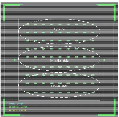
Figure 2.8: The designed Schottky diodes on a single wafer of GaAs. ... 27
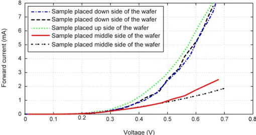
Figure 2.9: DC characteristics of Aluminum Schottky diodes placed at different side of the GaAs wafer. ... 28
Figure 2.10: The forward I-V curve of the chromium Schottky diode. ... 28
Figure 2.11: Comparison among different Schottky diodes. ... 29
Figure 2.12: (a): Mask of the designed planar Schottky diode; (b): Fabricated prototype of the planar Schottky diode. ... 29
Figure 2.13: (a): Planar Schottky diode; (b): Photoresist deposition; (c): Stabilizing the photoresist layer; (c): Expansion of the photoresist layer which causes the disconnection of the air-bridge. ... 30
Figure 3.1: General block diagram of a rectifier circuit. ... 32
Figure 3.2: Rectifier circuit topologies. (a) Single series-mounted diode. (b) Single series-mounted diode. (c) Voltage doubler. (d) Bridge diode. ... 34
Figure 3.3: Operation of voltage doubler rectifier. ... 35
Figure 3.4: Modified configuration of an up-microwave voltage doubler rectifier. ... 38
Figure 3.6: Real circuit model of a diode. ... 39
Figure 3.7: (a) Microstrip diode test mount, (b) Microstrip TRL calibration board. ... 40
Figure 3.8: Measured and simulated s-parameter (S12). Bias point V=0 V. ... 40
Figure 3.9: Optimized voltage-independent parameter of MA4E1317 Schottky diode. ... 41
Figure 3.10: Fabricated circuit of the 24 GHz voltage doubler rectifier. ... 41
Figure 3.11: Input matching of the 24 GHz voltage doubler rectifier. ... 43
Figure 3.12: Input matching of the 24 GHz voltage doubler rectifier. ... 43
Figure 3.13: RF-to-DC conversion efficiency versus input RF power. ... 44
Figure 3.14: Configuration of a self-biased rectifier. ... 45
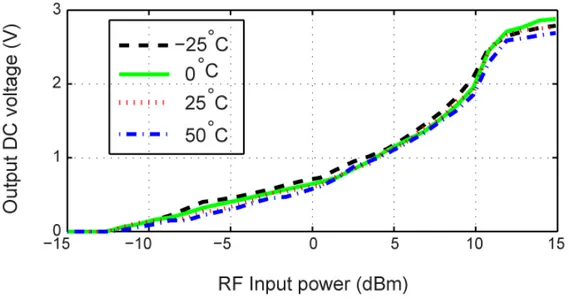
Figure 3.15: Simulated rectified voltage of the self-biased rectifier at different temperature. ... 45
Figure 3.16: Configuration of sensitivity improvement self-biased rectifier. ... 46
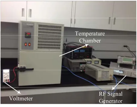
Figure 3.17: Measurement setup for the sensitivity improvement rectifier at different temperature. ... 47
Figure 3.18: Measured rectified voltage of the sensitivity improvement rectifier at different temperature. ... 48
Figure 3.19: (a) TRL calibration kit. (b) Fabricated rectifier without matching used for obtaining the input impedance of the rectifier. (A: reference plane, B: DC-pass capacitor, C: bias resistor, D: resistor load, F and E: Schottky diodes). ... 49
Figure 3.20: (a) Layout of the 24 GHz sensitivity improvement rectifier. (b) Fabricated prototype. Geometry parameters are following: Lf1 = 6, Lf2 = 4.24, Lf3 =2.66, Lm1 = 3.5, Lm2 = 3.3, Rg1 = 2.1, Lg1 = 4.6, Lg2 = 4.55, Lg3 = 6.9, Lg4 = 2.31, Lg5 = 2.24 (dimensions in millimeters). ... 49
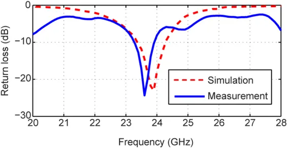
Figure 3.21: Simulation and measurement results of the 24 GHz sensitivity improvement rectifier return loss. ... 50
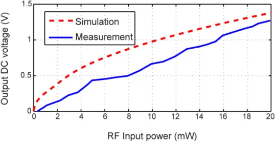
Figure 3.22: DC Output voltage versus input power of the 24 GHz sensitivity improvement rectifier. ... 51
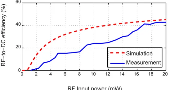
Figure 3.23: Maximum theoretical conversion efficiency (MTCE) versus input power of the 24
GHz sensitivity improvement rectifier. ... 51
Figure 3.24: Measured output DC voltage from two rectifiers; the self-biased rectifier and the improved configuration of the self-biased rectifier (thermal stability), versus input power. . 53
Figure 3.25: RF-to-DC conversion efficiency of the designed self-biased rectifier versus input power. ... 53
Figure 3.26: Rectifier simplified equivalent circuit. ... 55
Figure 3.27: Rectifier simplified equivalent circuit. ... 56
Figure 3.28: Power distribution at the output of the rectifier shown in Figure 3.27. ... 57
Figure 3.29: Output voltage of the rectifier shown in Figure 3.27. ... 61
Figure 3.30: Millimeter-wave harmonic harvesting rectifier. ... 62
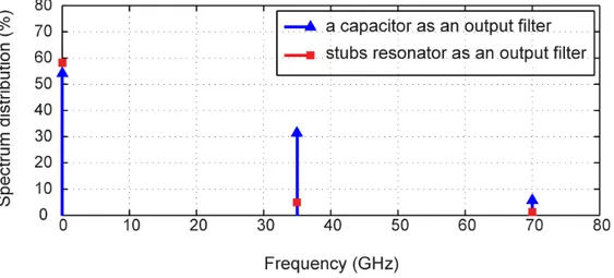
Figure 3.31: Distribution of the rectified signal and harmonics at the output of the voltage doubler (test point A) and harmonic harvesting (test point B). ... 62
Figure 3.32: Optimized voltage-independent parameter of MA4E1317 Schottky diode. ... 63
Figure 3.33: (a) Fabricated modified 35 GHz voltage doubler rectifier. (b) Fabricated 35 GHz harmonic harvesting rectifier ... 63
Figure 3.34: Simulation and measurement results of the harmonic harvester rectifier return loss. ... 64
Figure 3.35: Output DC power versus input RF power. ... 64
Figure 3.36: Rectifier efficiency versus input RF power. ... 65
Figure 4.1: Geometry and 3-D view of the (a) 1×4 antenna array, (b) 4×4 antenna array, and (c) power divider. ... 69
Figure 4.2: Microstrip to SIW transition. ... 69
Figure 4.3: Simulated |S11| and |S12| of the solid: microstrip to SIW transition, dashed: 1×2 T shaped power divider, and dotted: 1×4 power divider. ... 70
Figure 4.5: Measured and simulated impedances of the 4×4 array of SIW antenna ... 71
Figure 4.6: Simulated and measured radiation pattern in (a) E plane (YZ plane), and (b) H plane (XZ plane), of the 4×4 antenna array at 24 GHz, Solid: measured, dashed: simulated, and dotted: measured cross-polarization. ... 72
Figure 4.7: Fabricated circuit of the 24 GHz linearly polarized SIW rectenna. ... 73
Figure 4.8: Rectenna receiver power measurement setup. ... 74
Figure 4.9: (a) CP patch array antenna configuration. (b) Photograph of the fabricated prototype. Geometry parameters are following: R1 = 2.2, S1 = 0.65, W1 =0.45, L1 = 2.45, L2 = 2.35, L3 =
1.75, D = 8, L = 30 (dimensions in millimeters). ... 76
Figure 4.10: Simulation and measurement results of the CP array impedance matching from 22 GHz to 28 GHz. ... 76
Figure 4.11: Simulation and measurement results of normalized gain pattern of the CP array. (a)
XZ plane, (b) YZ plane. ... 77
Figure 4.12: Simulation and measurement results of the CP array impedance matching from 22 GHz to 28 GHz. ... 78
Figure 4.13: (a) 3D model of the SIW cavity-backed CP array. (b) Front-side of the fabricated prototype. (c) Back-side of the fabricated prototype. Geometry parameters are following: R2
= 1.85, S2 = 0.9, W2 =0.6, Rc = 1.9, Rv = 0.2 (dimensions in millimeters). ... 79
Figure 4.14: Simulation and measurement results of the SIW cavity-backed CP array impedance matching from 22 GHz to 28 GHz. ... 80
Figure 4.15: Simulation and measurement results of the normalized gain pattern of the SIW cavity-backed CP array. (a) XZ plane, (b) YZ plane. ... 81
Figure 4.16: Simulation and measurement axial ratios of the SIW cavity-backed CP array. ... 82
Figure 4.17: Comparison between measured axial ratio of the CP array and the SIW cavity-backed CP array. ... 82
Figure 4.18: (a) Front-side of the fabricated rectenna. (b) back-side of the fabricated rectenna. .. 83
Figure 4.20: Measured DC output voltage and efficiency versus incident power density of the
rectenna at distance of 1 m at 24 GHz. ... 85
Figure 5.1: General schematic of a self-powered transceiver. ... 87
Figure 5.2: Block diagram of a self-powered transceiver. ... 88
Figure 5.3: Three common configurations of a six-port junction. ... 91
Figure 5.4: Structure of an ideal Wilkinson power divider. ... 92
Figure 5.5: Structure of an ideal 90º hybrid coupler... 92
Figure 5.6: The layout of six-port junction. ... 94
Figure 5.7: The fabricated prototype of six-port junction. ... 94
Figure 5.8: Four-port measurement setup. ... 95
Figure 5.9: Matching and isolation conditions between RF and LO ports; (a): Simulation, (b): Measurement. ... 96
Figure 5.10: Matching conditions of output ports; (a): Simulation, (b): Measurement. ... 97
Figure 5.11: Transmission from RF port to outputs; (a): Simulation, (b): Measurement. ... 98
Figure 5.12: Transmission from LO port to outputs; (a): Simulation, (b): Measurement. ... 99
Figure 5.13: Phase transmission between LO port and outputs; (a): Simulation, (b): Measurement. ... 100
Figure 5.14: Phase transmission between RF port and outputs; (a): Simulation, (b): Measurement. ... 101
Figure 5.15: Analog front-end of six-port receiver. ... 102
Figure 5.16: System architecture of the proposed power harvester and date communication. .... 106
Figure 5.17: Common structure of a detector circuit. ... 107
Figure 5.18: RF-to-DC conversion efficiency for different Schottky diodes. ... 108
Figure 5.19: (a): Fabricated rectifier used to design the matching network; (b): Layout of the designed rectifier. ... 109
Figure 5.20: Matching condition of the designed rectifier. ... 110
Figure 5.21: Configuration of the modified detector used for simultaneous wireless energy harvesting and data communication. ... 110
Figure 5.22: Effect of the splitter power ratio on the constellation of the received signal. ... 111
Figure 5.23: Detection thresholds before and after power splitting. ... 112
Figure 5.24: ADS simulation of a conventional six-port detector. ... 113
Figure 5.25: Simulation results of DC voltage versus phase difference between the two input ports of a conventional six-port. ... 114
Figure 5.26: ADS simulation of the six-port with the function of harvesting and data communication. ... 114
Figure 5.27: Simulation results of DC voltage versus phase difference between the two input ports of six-port with the function of harvesting and detection. ... 115
Figure 5.28: ADS simulation of a conventional six-port receiver. ... 116
Figure 5.29: ADS simulation of the six-port receiver with the capability of simultaneous wireless power transmission and data communication. ... 116
Figure 5.30: Constellation of the demodulated QPSK signal. ... 117
Figure 5.31: Constellation of the demodulated 8PSK signal. ... 118
Figure 5.32: Constellation of the demodulated 16PSK signal. ... 118
Figure 5.33: Collected DC voltage at points V7 and H7 shown in Figure 5.29. ... 119
Figure 5.34: Collected DC voltage at points V8 and H8 shown in Figure 5.29. ... 119
Figure 5.35: Collected DC voltage at points V9 and H9 shown in Figure 5.29. ... 119
Figure 5.36: Collected DC voltage at points V10 and H10 shown in Figure 5.29. ... 119
Figure 5.37: BER performance of the ADS simulation for both receivers with QPSK modulation. ... 120
LIST OF ACRONYMS AND ABBREVIATIONS
AGC Automatic Gain ControlBPSK Binary Phase Shift Keying
CMOS Complementary Metal–Oxide–Semiconductor CP Circularly Polarized
EM Electromagnetic
ESD Electrostatic Discharge
HB Harmonic Balance
ISM Industrial-Scientific-Medical LHCP Left-Hand Circularly Polarized LNA Low Noise Amplifier
LO Local Oscillator LP Linearly Polarized
MHMIC Miniaturized Hybrid Microwave Integrated Circuit MPT Microwave Power Transfer
MTCE Maximum Theoretical Conversion Efficiency PCB Printed-Circuit-Board
PLF Polarization Loss Factor PSK Phase Shift Keying
QAM Quadrature Amplitude Modulation QPSK Quadrature Phase Shift Keying
RF Radio Frequency
RFID Radio Frequency Identification
SHC Sample-and Hold Circuit SIW Substrate Integrated Waveguide SNR Signal to Noise Ratio
SoC System on Chip
VNA Vector Network Analyzer WEH Wireless Energy Harvesting
WIT Wireless Information Transmission WPT Wireless Power Transmission
CHAPTER 1
INTRODUCTION
Presently, a large number of power-constrained wireless communication systems are used in various applications from portable entertainment systems to health care devices and wireless infrastructures. These systems are typically powered by batteries that have a limited operation time and they have to be replaced or recharged in order to guarantee the operation of a network for a certain period of time. However, the procedure of battery replacement or recharging may create an undesired expenditure and sometimes is not practical or readily unavailable (e.g., implant devices inside human bodies or for sensors embedded in building structures). Hence, harvesting energy wirelessly from the environment can be a promising solution in providing long-lasting energy supplies for energy-constraint power-limited wireless communication systems. Usually, solar and wind are the well-known renewable energy sources for energy harvesting which may not be available continuously according to the environment, location and weather conditions. Therefore, scavenge energy from ambient RF signals can be a potential alternative in generating clean and renewable power source. Therefore, harvesting RF energy can be a viable new source for wireless power charging and battery-free solutions in many existing and emerging applications such as RF identification (RFID) and wireless sensor networks (WSN) [1].
On the other hand, it is well known that one of the most important concerns in communication systems is their power consumption so that extensive researches are being focused to reduce the required power level of wireless communication systems through the design of low-power receiver techniques. Moreover, to develop wireless communication systems, simple structure, compact-sized, low-cost and wideband transceivers are also points of interest. Considering those mentioned requirements, multiport receiver techniques based on the principle of interferometer are more practical compared to the other existing receiver configurations since their simple architectures can address most of the above-mentioned issues [2].
Besides, RF techniques have been instrumental for wireless information transmission (WIT). Therefore, since these signals that carry energy can at the same time be used as a vehicle for transporting information, simultaneous wireless power transmission (WPT) and data communication becomes an interesting new area of research that attracts increasing attention toward the development of self-powered receivers. Consequently, in this thesis we have conducted research on the far-field WPT and developed rectennas and wireless receivers with the capability
of energy harvesting and data at the same time in such a way to use the same transmitted electromagnetic (EM) wave to transport both energy that is harvested at the receiver, and information that is decoded by the receiver.
1.1 State-of-the-art of the wireless receiver capable of energy
harvesting
1.1.1 Far-field wireless power transmission
Wireless power transmission is considered as a three-dimensional means of transferring electrical power from one place to another. In general, there are three basic wireless powering techniques, namely; short-range induction technique, mid-range magnetically coupled resonance technique and long-range far-field rectification technique [3]. The short-range induction technique is normally used at the maximum distance of a few centimeters. In this technique, the electric current through a primary coil generates a magnetic field which on a secondary coil results in generating a current therein. Two coils are electrically isolated from each other and the transfer of energy takes place by electromagnetic coupling through a process known as mutual induction (non-resonant induction). Over greater distances and when the coils are placed a few meters apart, the non-resonant induction technique is inefficient and wastes much of the transmitted energy just to increase range. An efficient power transmission in this case can happen if the electromagnetic fields around the coils resonate at the same frequency (coupled resonance) which transfer a stream of energy from the transmitting coil to the receiving coil. This technique is a non-radiative energy transfer since it involves stationary fields around the coils rather than fields that spread in all direction.
The long-range wireless power transmission is completely different from the two previous methods and this thesis work focuses on this method of energy transfer. This technique is mostly related to the development of rectennas. The rectenna, the rectifying circuit integrated with an antenna, is the most important module in long-range WPT, whose development has been reviewed in [1], [4]-[6]. The overall performance of a WPT system is normally determined by the efficiency of both the antenna and the related rectifier circuit. Then, it is essential to design high-efficiency rectennas to guarantee the quality of the WPT system.
Until now, most rectenna elements and rectenna arrays have been developed for frequencies below 10 GHz, especially for the ISM (Industrial-Scientific-Medical) bands. Various configurations of wireless rectennas operating at low microwave frequencies; such as 915 MHz and 2.45 GHz, are widely available in the literature [7]-[9]. In general, wireless rectennas are studied from two points of view, namely; operating frequency and RF-to-DC conversion efficiency. For example, a rectenna with 85% and 82% RF-to-DC conversion efficiency operating at 2.45 and 5.8 GHz, respectively, was presented in [7]. The rectennas operating at low frequencies normally aim at harvesting the ambient energy from abundant Wi-Fi and other wireless signal sources. For low-frequency operation, the antenna structure may be limited by its physical and aperture size although ambient electromagnetic power density is relatively high at commonly used wireless frequencies due to its wide-spread deployment for commercial applications and its relatively low-cost wireless power source generation.
So far, only a few rectennas have been reported for the millimeter-wave operation and most of them have focused on single element performances. A rectenna operating at 10 GHz and 35 GHz with respective 60% RF-to-DC conversion efficiency at 140 mW input power and 39% RF-to-DC conversion efficiency at 120 mW input power were presented in [10]. Recently, some studies have been done at 24 GHz [11]-[14]. For instance, [12] describes a rectifier with 54% of efficiency driven by 130 mW input power and 41% with 50 mW. Although the state-of-the-art efficiency of rectennas reported so far is still low at millimeter-wave frequency, the advantages of absolute size reduction and potential high-power density make them more attractive in terms of overall system efficiency for pin-point long-distance wireless power delivery. The development of wave harvesters is also driven by ever-decreasing cost and increasing popularity of millimeter-wave technologies and applications including CMOS developments [15] and [16]. A CMOS rectenna operating with efficiency of 53% at 35 GHz and 37% at 94 GHz was reported in [15].
1.1.2 Multiport technique
The multiport interferometer technique was first analyzed in the 1970s by Engen and Hoer in order to propose an accurate power measurement setup [17], [18]. Shortly after its initial publication, the principle was expanded to the characterization of voltage, current, impedance, and phase, resulting in an alternative network analyzer approach [18]. Based on these concepts, a
variety of different applications has been proposed which proves the universal nature of the basic multiport concept [19].
1.1.2.1 Multiport applications
As mentioned above, the multiport circuit technique can be used in microwave network measurements, since it is capable of providing a low-cost measurement of amplitude and phase. Besides, the multiport, in addition to network parameters, can realize power measurements. Using the multiport technique provides a simultaneous power flow and impedance measurement with no need of phase measurements. A detailed description of microwave network measurement could be found in [20] and [21]. Moreover, the multiport technique has many other applications in microwave and millimeter-wave systems where measuring the phase and amplitude of the signal is required such as directional finder, reflectometer and antenna measurement. Multiport reflectometer for measuring the reflection coefficient of a load has been described in [17]. Also, there is a great potential in radar application especially in the automobile industry where low-cost and high performance radar is needed [22]. Furthermore, since the multiport architectures feature low-cost, long-term stability, dynamic range of up to 50 dB, they appear to be suitable for antenna measurement including the near field and polarization [23], [24]. The multiport technique is also used to perform non-destructive permittivity measurements. This technique is appropriate for measuring relatively high-loss dielectric liquids [25]. In addition, the multiport technique has applications in optical systems. The early investigation on the use of a six-port architecture in optics was an optical reflectometer used for measuring optical complex reflection coefficients [26]. An important advantage of this architecture compared to other techniques is the capability to handle high-power signals, enabling the setup of large-signal analysis systems for power amplifier or semiconductor circuits [27].
1.1.2.2 Multiport receiver
The concept of multiport receiver was first introduced in 1994, which has stimulated an important development in wireless receiver design [28]. The underlying multiport receiver principle of operation is related to the additive mixing or coherent interference of radio frequency (RF) and local oscillator (LO) signals through a passive network with a couple of controlled relative phase and amplitude outputs for a direct down conversion through diode power detectors or power
reading. Therefore, the multiport receiver allows increasing the upper frequency limit and decreasing the required power because of the utilization of power detectors instead of mixers.
Professors R.G. Bosisio, Ke Wu and S. O. Tatu who are the pioneers in developing the multiport technique, introduced the up-microwave and millimeter-wave applications of six-port demodulator in connection with homodyne and heterodyne receivers [29]. Since then, the multiport technique has been widely studied and used as an alternative for direct conversion transmitter and receiver for modulating and demodulating signals in different modulation schemes, such as, binary phase shift keying (BPSK), quadrature phase shift keying (QPSK), and quadrature amplitude modulation (QAM).
1.1.2.3 Comparison between multiport receivers and conventional receivers
The six-port receiver has several advantages over its conventional counterpart. First of all, the broadband specifications can be easily obtained by building passive elements. Moreover, the homodyne technique based on the power detection ensures relatively low power consumption because of a relatively low driving power level. In addition, its hardware architecture is simple and cost-effective. Therefore, the multiport based receivers are an expedient enhancement to the group of the available receiving topologies. Especially for high frequencies and large bandwidths, they have been demonstrated as an excellent alternative to the common architectures [30]. To enable a serious validation of the multiport technology, a benchmark has been done between the six-port receivers and the existing receiver architectures from several points of view [31], [32].
1.1.2.4 RF performance
Phase accuracy: In conventional receivers, the phase noise of the local oscillator (LO) is
directly converted to the phase noise in the complex baseband. This phase noise leads to a neighbor channel interference, caused by reciprocal mixing, and thus reduces the selectivity of the receiver. In the case of the direct conversion receiver and six-port receiver, an additional phase inaccuracy is introduced because of the inaccurate calibration. With this unavoidable phase imbalance, a phase distortion is generated [33].
Noise figure: The noise figure is usually defined by the LNA stage of a receiver. If no LNA
is used in the structure of the receiver, the noise of a mixer is comparable to the noise of a power detector. For frequencies beyond 50 GHz, both are usually built up using Schottky diodes. The
noise figure for diode mixers is close to its conversion loss which is typically about 7 dB [34]. Simulations on microwave power detectors using a beam lead GaAs Schottky diode have shown that the noise figure can be lower than 4.8 dB for input power smaller than -20 dBm.
LO power: For most mixers, to obtain a good conversion loss, the LO power should be in
the range from 0 to 10 dBm [34]. In the six-port receivers, a suitable condition is a LO power in the area of the receiver input power which is much lower in practical applications (less than -10 dBm).
In-band dynamic range: The dynamic range of six-port receiver is mainly determined by
the accuracy of calibration and detector sensitivity. First trials have shown a dynamic range of 40 dB [35], [36]. It must be noticed that the calibration limits the linearity of the receiver. The dynamic range of mixer based receiver is limited by the linearity and 1 dB compression point of -10 dBm to 10dBm. This results in a dynamic range of about 90 to 100 dB for a signal bandwidth of 10 MHz. The dynamic range of the receivers can be improved up to 70 dB using an AGC inserted within the LNA [29].
Self-mixing effects: Direct coupling and external reflections can cause a DC offset in the
direct conversion receivers and six-port receivers since the desired baseband signal as well as the unwanted DC offset are both centered at DC, therefore they cannot be separated by filtering. The six-port receivers are less sensitive to the DC offset because this problem is mitigated by the calibration procedure, but the direct conversion receivers contain some signal processing unit to cope with this effect [32].
1.1.2.5 Constraints
Size: Major part of a mixer-based receiver is occupied by active components and filters which
are large in size and cannot be integrated on the chip while the usual size of a six-port is about 3
4
in square, and for V, W and D band applications, it is possible to integrate the six-port on a chip.
Cost: The cost of a direct conversion receiver depends on the frequency range. At high
frequencies especially in D and W band, mixers are expensive and in some cases they are rare whereas power detectors are available for higher frequencies. For millimeter-wave signal generation, usually a lower frequency LO is followed by a frequency multiplier, which produces a
small LO power. The six-port receivers will have a cost advantage by reducing the LO power requirements.
According to the above comparisons and discussions, it is clear that the six-port receiver is a suitable and cost-effective alternative to the existing systems, especially for millimeter-wave applications. At millimeter-wave frequencies, the neighbor channels interference are negligible so the reduced dynamic range is acceptable. In addition, it has been proved that the six-port receiver architecture is less sensitive to LO power variations and phase errors than the antiparallel diode receivers [32].
1.2 Motivation and research objectives
Therefore, according to the above-mentioned backgrounds, the need for a high efficiency rectenna operating at millimeter-wave frequency as well as a proper architecture of low-power wireless receiver design have motivated our research to realize a quality receiver for simultaneously wireless power transmission and data communication.
The overall objective of this thesis is to develop a wireless receiver for simultaneous wireless power transmission and data communication using the multiport technique. To be more specific, there are three main objectives as follows:
1. To investigate different configurations of a rectifier circuit and to propose a simple architecture with high RF-to-DC conversion efficiency operating at up-microwave and millimeter-wave frequency under low/medium RF power level;
2. To determine specifications required for antenna selection in regards to WPT applications and to design a high gain millimeter-wave rectenna array;
3. To propose a new structure for the six-port receiver in order to present an innovative receiver with the capability of simultaneous wireless power transmission and data communication.
1.3 Methodology
1. The required conditions to design the rectifier circuits (using Schottky diode) with high RF-to-DC conversion efficiency are examined in terms of appropriate diode selection and circuit design. It is well known that the maximum efficiency of Schottky diode rectifiers is limited by the maximum operating frequency and the loss of the system. Therefore, the internal analysis of Schottky diodes dealing with rectifying element characteristics as well as the external analysis considering the component modeling and matching effects are investigated in detail.
2. Various architectures of rectifier are studied from the points of view of the required RF power and operating frequency. Then, the common structures of rectifiers are modified to make them operational at up-microwave and millimeter-wave frequency. Consequently, three different structures of high efficiency rectifier operating at 24 GHz and 35 GHz are designed and their performance are examined experimentally.
3. Different antenna configurations are investigated with regards to the required specification for WPT applications such as gain, polarizations, weight and fabrication techniques. Since, in a WPT system, an antenna plays an important role in receiving RF power, then its performance is a critical factor in determining the overall efficiency of the system.
4. Considering the required criteria for a WPT antenna, a proper structure of WPT antenna array operating at 24 GHz is designed and experimentally tested. Then, it is integrated into the designed low-power rectifier to realize the WPT rectenna.
5. To validate the idea of a system with the capability of simultaneous wireless power transmission and data communication, different configurations of wireless receiver are studied. Considering the desirable requirements of a wireless receiver such as low-power consumption, compact-sized and low-cost, the use of a multiport technique is an appropriate solution that addresses all the above-mentioned concerns. Figure 1.1 shows the flowchart of the proposed system to provide wireless power transmission and data communication at the same time using the six-port technique. Since it is shown in Figure 1.1, the detector module of the six-port receiver, should have a special design which can
RF received signal
Six-port
junction Rectifier
Wireless Energy Harvesting
Baseband signal processing unit
Power management unit
Data Communication Unit Voltage divider
network
Differential amplifier Detector
Figure 1.1: Flowchart of simultaneous wireless energy harvesting and data communication. split the generated DC voltage with a specific ratio in order to harvest the energy and perform the data detection.
6. Since the designed six-port junction is used in a power harvesting structure, it has to have the minimum passive loss to transfer as much as possible RF power to detectors. To do so, one with the lowest loss is selected among the different configurations of six-port junction, designed and optimized to operate at the desirable frequency (24 GHz in this case).
7. The detector of interest has to generate more DC power, therefore it should act as a rectifier with a high RF-to-DC conversion efficiency. This rectifier is designed considering the required conditions such as low-power (maximum power of 10 dBm), operating at up-microwave frequency (24 GHz) with the ability of dividing the generated DC power with a specific ratio.
8. After the detection module, some part of the DC voltage is transferred to the differential amplifiers to realize the I and Q data detection (analog signal detection [37]) while the rest is harvested.
1.4 Original contributions
The original contributions of this thesis can be summarized in the following:
A self-biasing technique is presented as an efficient approach to reduce the required power of rectifiers and design low-power rectifier circuits. To justify the claim, a 24 GHz self-biased rectifier is designed and prototyped. The measurement results
show that the self-biased rectifier is more efficient than the conventional designs when the available RF power density is low.
In order to increase the efficiency of the rectifiers, an original idea is put forward to harvest harmonics generated by the nonlinear rectification process in the millimeter-wave rectifier. To validate the proof of concept, a 35 GHz harmonic harvester rectifier is designed, fabricated and experimentally tested. The measured efficiency has the maximum value compared to the conventional rectifiers (without harmonic harvesting or recycling) reported in the literature.
A robust investigation of up-microwave and millimeter-wave rectennas is presented to maximize the harvested DC power. Consequently, a 24 GHz compact rectenna is developed to demonstrate the feasibility of wireless power harvesting and transmission techniques towards millimeter-wave regime. To the best of our knowledge, the designed rectenna has the highest efficiency reported to date compared to the previous studies.
An original idea of simultaneous wireless power transmission and data communication is presented. The proposed system is based on the six-port technique in connection with a special architecture of rectification circuit which acts as a detector and also a rectifier both to achieve data extraction and high efficient RF-to-DC rectifying functions.
In summary, this thesis addresses all the design issues from system-level analysis to component-level design, from CAD simulation to experimental validation and from original idea to prototype implementation.
1.5 Thesis outline
This thesis details research works performed on planar modeling of Schottky diode and fabrication procedure, nonlinear rectifier circuit analysis, rectenna design issues for applications of wireless energy harvesting, and finally a system of simultaneous wireless power transmission and data communication. The thesis is organized as follows:
Chapter 2 provides a general description of the Schottky diode technology. It initiates with the basic diode operating principle, and further discusses the issues specifically related to the planar diode structure. At the end, the diode design, optimization and fabrication principles for rectifier applications as well as the simulation and measurement results are presented.
Chapter 3 develops an analysis of nonlinear rectifiers and derives the required conditions to achieve a maximum efficiency rectification. It begins with a review of different configurations of rectifier and then explains the design steps to realize an up-microwave/millimeter-wave rectifier with a maximum RF-to-DC conversion efficiency. A 24 GHz voltage doubler rectifier is designed and experimentally tested. The self-biased technique is presented as a method to reduce the required input RF power and consequently design a low-power rectifier. A self-biased rectifier is developed and prototyped at 24 GHz to justify the claim. Finally, the harmonics generated through the rectification process are investigated using some analytical approach based on Ritz-Galerkin (RG) technique. It is shown that some parts of power are wasted in harmonics which are normally filtered out by some DC-pass filtering after passing through the Schottky diode, then the idea of harmonic harvesting is introduced to increase the overall efficiency. To validate the idea, a 35 GHz harmonic harvester rectifier is designed, optimized and fabricated.
Chapter 4 addresses the integration issues between rectifiers and antennas to realize rectennas for wireless powering. Various configurations of antennas are studied considering WPT applications. Subsequently, two rectennas are designed and experimentally demonstrated on the example of a linearly polarized SIW slot array with a voltage doubler rectifier and a circularly polarized SIW cavity-backed in connection with a self-biased rectifier. Calibration, circuit validation, impedance matching to nonlinear impedances, DC collection circuit design and integrated rectifier-antenna characterization are all presented in detail.
Chapter 5 presents the idea of a simultaneous wireless energy harvesting and data communication system based on the multiport interferometer technique. This chapter begins with a brief review of different configurations of wireless receiver and it explains the reason of choosing the multiport technique to design such a system. Consequently, different structures of a six-port junction are studied and their related s-parameters are extracted. A proper configuration of six-port junction operating at 24 GHz is designed and prototyped using our in-house miniaturized hybrid microwave integrated circuit (MHMIC) technique. The designed six-port is used to build up the
receiver. Then, the design process of a special detector module with high RF-to-DC conversion efficiency is explained. Next, the designed detector is connected to the six-port outputs to realize the receiver. Finally, the ADS simulation of the six-port receiver featuring both power harvesting and data detection is presented and its performance in terms of constellation points and BER are compared to the conventional counterpart. The simulations start with the ideal component models provided in ADS and end up with much more realistic models obtained in EM simulations and measurements.
Chapter 6 summarizes the thesis work with a concise conclusion and gives some future directions of our research in this interesting area of microwave engineering.
CHAPTER 2
PLANAR SCHOTTKY RECTIFIER DIODES
Generally, a Schottky diode can be used in designing mixer, detector or rectifier circuits. However, the required features for a mixer Schottky diode differ from the required specifications for a rectifier Schottky diode. Moreover, microwave rectification using Schottky diode has been widely discussed in the context of energy harvesting and WPT. Therefore, in this chapter we intend to have a closer look at rectifier Schottky barrier structure by itself, to understand about the nature of rectification. Even though, the commercial Schottky diodes have been used in our fabricated WPT systems.
In 1904, the first practical semiconductor device was introduced and in fact it was a metal-semiconductor contact which showed a certain rectifying behavior. In 1938, Schottky suggested that the rectifying behavior could arise from a potential barrier [38]. This was later named as Schottky diode. Since Schottky diodes play an important role in the development of high frequency electronics as rectifier especially for millimeter-wave rectification, this chapter provides an overview of the Schottky diode operation. Therefore, general physics of the metal-semiconductor interface forming a Schottky barrier and the corresponding diode equivalent circuit model are discussed briefly. Consequently, the diode operation as a rectifier is described and the design parameters for rectifier and performance optimization are given. Furthermore, some initial results of our in-house fabricated prototypes of a planar rectifier Schottky are presented.
2.1 Summary of Schottky diode operation
When a metal makes contact with a semiconductor, a barrier is formed at the metal-semiconductor interface. The fundamental operation of a Schottky diode is regarded to carrier transport mechanism over a Schottky barrier. This barrier is responsible for controlling the current conduction as well as its capacitance behavior. The metal-semiconductor interface and the corresponding diode terminal notation is presented in Figure 2.1.
In designing the Schottky diodes, both n-type and p-type semiconductors can be used. In n-type Schottky barriers, the forward current results from electron movement from the n-type semiconductor into the metal while in p-type Schottky, the forward current drives from holes movement from p-type semiconductor into the metal.
Vd Anode Cathode Anode Cathode Depletion region Metal n-GaAs (a) (b)
Figure 2.1: (a): Symbol of a diode; (b): Metal-semiconductor interference in a Schottky diode.
Since in Schottky diodes only one type of semiconductor (n-type or p-type) exists, therefore slow and random recombination of n-type and p-type carriers does not happen. For this reason, Schottky diodes are much faster in conduction and unlike junction diodes, they do not have any delay effect due to the charge storage. It means that, in Schottky diodes, when the forward voltage is removed, the current flow stops instantly and reversed voltage is established in a few picosecond [38].
2.1.1 Metal-semiconductor contact [38]
According to Figure 2.2, when the metal and the n-type doped semiconductor are separated from each other, the metal-semiconductor band diagram looks completely different from the band diagram of the time they are in contact. In an intimate contact, electric charge will drift from the semiconductor to the metal and a thermal equilibrium is stablished. The Fermi level on both sides will line up. Relative to the Fermi level in the metal, the Fermi level in the semiconductor is lowered by an amount equal to the difference between the two work functions. This band diagram is explained in detail in [38]. In the thermal equilibrium condition, the semiconductor region next to the metal contact is depleted of electrons and electron movement from the semiconductor to the metal is blocked by an energy barrier, identified as built-in-potential,
bi. By changing the potential between the metal and semiconductor, i.e., when an external bias is applied over the diode terminals, the width of the depletion layer d( )Vj as well as the built-in potential is changed.ϕm ϕs Eg Ec Ef χs Ef Ev Vacuum Vacuum level Metal Semiconductor
(a)
ϕm ψbi Eg Ec Ef χs Ef Ev Vacuum level ϕb Metal Semiconductor(b)
ψbi E c Ef ϕb Metal Semiconductor Surface states(c)
For an ideal contact, a barrier height
b is calculated as the difference between the metal work function
m and semiconductor electron affinity
s.
b is an important factor as it determines theLO power required to bias the diode in its nonlinear region. In many millimeter-wave applications, the LO power is at premium and, therefore, low barrier Schottky diodes are desired. In practice, the barrier height dependency on metal work function is weak compared to the ideal case. Experimental characteristics showed that the estimation of a practical barrier height is rather complicated [39]. The physics of the metal-semiconductor system can be found in the literature [40]-[46].
Table 2.1 shows some experimental values of barrier height of different Schottky diodes ranging from 0.15 to 0.9 V [47].
Table 2.1: Experimental values of metal-semiconductor barrier height in volts
Metal b
Si (n-type) (111) (V) b
Si (p-type) (111) (V) b
GaAs (n-type) (100) (V) Au 0.81 0.9 Ni 0.3 0.8 Mo 0.6 Ti 0.35,0.5 0.61 W 0.69 Ag 0.69 0.88 Pt 0.85 0.86 Pt-Ni Alloy 0.6 Pd 0.72 0.15-0.25 Au-Ge 300ºC 0.27 Au-Ge 200ºC 0.352.1.2 Schottky diode material
Schottky barrier diodes are generally fabricated from n-type silicon (Si) or n-type gallium arsenide (GaAs) epitaxial layer. For up-microwave and millimeter-wave applications, n-doped GaAs is more desirable due to its high electron mobility (8000 2
. cm
V s for doping concentration
of 1018c m3), relatively low current leakage through the Schottky barrier, ready availability, wide
bandwidth and room temperature operation. Also, there has been a considerable interest in using some of the other, even higher mobility, III-V compounds, but there have been practical difficulties in deploying them. One of the most promising materials is indium antimonide (InSb) with mobility
nine times higher than GaAs. According to the literature, some Schottky barrier diodes were fabricated on InSb, showing an enormously high series resistance in addition to a relatively low shunt resistance [48]-[49]. One of the drawbacks of InSb is its low band gap requiring that it be cooled to produce a rectifying barrier. The other common semiconductors used in the fabrication of Schottky diodes are gallium nitride (GaN), silicon carbide (SiC), indium phosphide (InP) and indium gallium arsenide (InGaAs). Examples of metals used for the Schottky anode contacts are titanium (Ti), platinum (Pt), chromium (Cr), tungsten (W), molybdenum (Mo), and various alloys. The typical metal (ohmic) contact is an alloy of Ge, Au and Ni since they decreases contact resistance to n-GaAs. The choice and processing of materials result in a low series resistance along with a narrow spread of capacitance value for close impedance control.
Moreover, the epitaxial layer to be used must have the following main important properties: 1. The correct crystallographic orientation (100) for GaAs and (111) for Si in order to
avoid the uncertainties and patchy result characteristics of using a polarized crystal face, 2. A very low crystallographic imperfection density in order to ensure the minimization of
avalanche noise,
3. Excellent surface morphology to allow for submicron device dimension,
4. The correct epitaxial layer doping level, abrupt interface and thickness to ensure the lowest possible device series resistance and the highest possible cutoff frequency. In addition to the correct epitaxial layer properties mentioned above, the epi-layer thickness should not be greater than 2000˚A for the optimum device design, since it effects on the series resistance and forward voltage drop of the diode. Also the resistivity of the substrate needs to be
Vd Anode Cathode Anode Cathode Depletion width Metal (a) Repi Rbuf Rohmic Rs n++ GaAs Buffer layer n- GaAs Ohmic contact
V
d (b) Id Rj(Vj ) Cj(Vj ) Rs(Vf )Figure 2.3: (a): Cross-section view of a GaAs Schottky diode; (b) Equivalent circuit model. as low as possible, more desirable less than 0.001cm, to minimize the contribution of substrate series resistance
R
s,
which is explained in the sequel.2.1.3 Schottky diode circuit model
A cross-sectional view of a GaAs Schottky diode shown in Figure 2.3 contains three main layers; the epi-layer, the buffer layer and the ohmic contact. Normally, the buffer layer is made of a high doped GaAs (with doping concentration more than 1018c m3) to ease the current flow from
the epi-layer to the ohmic contact. The current flow between the semiconductor and the external circuit is made through the ohmic contact.
The equivalent circuit model of the Schottky diode shown in Figure 2.3 (b) consists of a voltage-dependent current source, Ij(Vj) charge source, Qj(Vj) and a series resistor Rs. The diode
essential properties are dependent on junction voltage, Vj. The series resistor, Vj, is the sum of the
resistance due to the epitaxial layer, Repi the resistance due to the current spreading through the
buffer layer, Rbuf and the resistance due to the semiconductor-ohmic contact, Rohmic. But the major
contribution comes from Repi and Rbuf. The series resistance in the epitaxial layer and the buffer
depends on the junction geometry, frequency, and to a lesser extent, on the applied voltage. Therefore, Rs is given by
( , )
( , )
( )
s j epi j buf
where 2 ( ) epi e d w R A q N A
(2.2) 2 2 buf buf A R d (2.3)in which
is the epitaxial layer resistivity,w
is the epitaxial thickness, Ais the size of the Schottky contact,
eis the electron mobility of the epitaxial layer (this assumes the layer is n-type), andN
dis the donor density in the epitaxial or active layer.
buf is the buffer resistivity and d isthe active junction diameter (in case of having a circular Schottky contactd 2 A
).
However,
R
epiis a voltage-dependent parameter, but its voltage-dependency is not strongand the series resistance is normally considered as an extrinsic element.
2.1.4 Current-voltage characteristic
Under a forward bias condition, thermionic emission, recombination in the space charge region and recombination in the neutral region occurs in the current transport mechanism [50].For a good quality metal-semiconductor contact, the majority of the carrier transport is caused by thermionic emission. Thermionic emission in a Schottky contact has been discussed in detail in [40] and [43]. The current-voltage (I-V) equation of a Schottky diode is described by
( , )
(
1)
j B qV k T j s dI V T
I e
(2.4) where ** 2 ( ) b B q k T s I T AA T e (2.5)in which
I
dis the diode junction conduction current,I
sis the saturation current,V
jis the junctionvoltage,
is the ideality factor of the diode, q is the electron charge (1.6 10 19Coulomb), Bk
isBoltzmann’s constant (1 .3 7 1 0 2 3 J
K
),T is the absolute temperature, Ais the Schottky contact area, A**is the effective Richardson’s constant ( 2 2
8.2 A cm K for GaAs) and
bis the barrier height.In the forward condition when the thermionic emission dominates the electron transport mechanism, the ideality factor is close to unity. But in the practical scenario, this is not the case and the ideality factor depends on the doping concentration and the temperature as well [51]. Therefore, the ideality factor is described by
00 00 1 tanh( ) 1 ( ) 2 B B B E k T k T E E (2.6) 12 00 18.5 10 * d e r N E m (2.7)
whereE is the material constant in eV , 00 E is the band bending, B * e
m
is the electron effective mass in unit of free electron mass, N is the epi-layer doping concentration in d c m3 andr
is the semiconductor relative permittivity.Under the reverse-biased condition, the semiconductor area under the metal contact is depleted of electrons and the ionized donors occupy this region. When the diode junction goes under a reversed-biased, the electric field across the junction increases and the electron conduction current decreases. In theory, under reverse-biased conditionVj , Id . While in reality, Is a high reverse-bias voltage causes a high electric field across the junction resulting the junction to breakdown. The breakdown voltage,
V
br,
is estimated as3 3 2 4 16 60( ) ( ) 1.1 10 g d br E N V (2.8)
where
E
g is the band gap energy in eV and N is the epi-layer doping concentration in d c m3 [38].2.1.5 Capacitance-voltage characteristic
While the depletion region is emptied of electrons, using Poisson’s equation can determine the diode capacitance-voltage (C-V) relation as
0 ( ) 2 1 j j j j bi b i V Q V C (2.9) 0 ( ) ( ) j j bi j j j j bi j dQ V C V C dV V (2.10)
where,
C
jois the zero-biased junction capacitance given by [52]2 s d jo bi q N C A (2.11)
in which
sis the semiconductor dielectric constant.On the other hand, a diode can be considered as a parallel plate capacitor where the distance between two plates is the width of depletion region,
w V
d( ),
j which is controlled by the junction voltage. ( ) ( ) s j j d j A C V w V (2.12) while 2 ( ) ( ) s bi j d j d V w V qN (2.13)The mentioned equations are valid in the condition of absence of electron in the depletion area. Under a forward-biased condition, the conduction current of electron increases which affects the carrier distribution. Therefore, under such a condition, the diode junction capacitance is calculated using a numerical solution of semiconductor transport equations [53].