HAL Id: inria-00446064
https://hal.inria.fr/inria-00446064
Submitted on 12 Jan 2010
HAL is a multi-disciplinary open access
archive for the deposit and dissemination of
sci-entific research documents, whether they are
pub-lished or not. The documents may come from
L’archive ouverte pluridisciplinaire HAL, est
destinée au dépôt et à la diffusion de documents
scientifiques de niveau recherche, publiés ou non,
émanant des établissements d’enseignement et de
Efficient Dynamic Reconfiguration for Multi-context
Embedded FPGA
Julien Lallet, Sébastien Pillement, Olivier Sentieys
To cite this version:
Julien Lallet, Sébastien Pillement, Olivier Sentieys. Efficient Dynamic Reconfiguration for
Multi-context Embedded FPGA. 21st Annual Symposium on Integrated Circuits and System Design,
SBCCI’08, 2008, Gramado, Brazil. pp.210-215, �10.1145/1404371.1404428�. �inria-00446064�
Efficient Dynamic Reconfiguration for
Multi-Context Embedded FPGA
Julien Lallet, S´
ebastien Pillement, Olivier Sentieys
IRISA, University of Rennes,
6 rue de kerampont, 22300 Lannion, France.
email:{lallet, pillemen, sentieys}@irisa.fr
January 12, 2010
Abstract
Dynamic reconfiguration on fine-grained architecture can only be reached by multi-context FPGAs when reconfiguration time is a critical issue. Un-fortunately the multiple contexts bring power and area overhead. This pa-per introduces the Dynamic Unifier and reConfigurable blocK (DUCK), a new structure to perform efficiently dynamic reconfiguration. The DUCK allows to separate the configuration path and the configuration registers which facilitates simultaneous configuration and computing steps. The reconfiguration process using the DUCK concept is presented in detail and synthesis results are given for different structures. Our solution is finally validated with the implementation of a WCDMA receiver on a multi-context embedded FPGA and demonstrates the interest and the efficiency of using dynamic reconfiguration.
1
Introduction
Systems on Chip (SOC) are based on three main kinds of architecture. First, Application-Specific Integrated Circuits (ASIC) allow to efficiently compute an algorithm due to dedicated hardware but are unfortunately inflexible. Secondly, processors are the most flexible architectures, but compute in an inefficient way. Finally, static reconfigurable architectures such as Field Programmable Gate
Area (FPGA) are considered a good compromise between processors and ASIC. Meanwhile, mixed architectures have been developed in order to improve the efficiency and the performance of processors by the use of static reconfigurable co-processors. These static reconfigurable co-processors embedded into a SoC, namely embedded-FPGA (e-FPGA), have allowed processors to follow appli-cation developments. Dynamic reconfiguration allows partial configurations at run-time, and thus improves performances. Multi-context FPGAs take advan-tage of dynamic reconfiguration in their architecture. This is achieved by the local storage of any possible context. When a new configuration is required, the system switches between one or the other context. The major drawback of this solution is the silicon area and power inefficiency caused by local memories needed to store all the contexts. Furthermore, to our knowledge, no e-FPGA with efficient dynamic reconfiguration features has been developed until now. Our contribution to multi-context FPGA is the definition of an optimized struc-ture that supports dynamic, partial and run-time reconfiguration. This is per-formed by only two configuration memories, one current configuration memory and one parallel configuration memory. The parallel configuration memory is used for loading or saving context for preemption to or from the configuration memory in on one clock cycle. New contexts are stored in this parallel config-uration memory thanks to a splittable scan-chain. Compared to multi-context FPGA, configurations exploit efficiently the available silicon resources.
The paper is structured as follows. Section 2 describes related works on opti-mization of multi-context FPGA. Section 3 presents our contribution on dynam-ically reconfigurable e-FPGA. In Section 4, we present the experimental method and discuss results on a WCDMA receiver implementation on an e-FPGA. Fi-nally, Section 5 sums up this paper.
2
Related Works
For a decade, many dynamically reconfigurable architectures have been devel-oped, mainly reconfigurable processors. The only fine-grain architectures which implement dynamically reconfigurable computing are multi-context FPGA. In-dustrial FPGAs (e.g. Xilinx Virtex family) allow dynamic reconfiguration, but the reconfigured resources have to be stopped before a new configuration can be propagated. Different approaches have been proposed in the literature to
re-duce the excessive silicon area used by multi-context FPGAs. First, some works focus on the reduction of the configuration words. In [1], the method consists in the limitation of the connection map inside a switch box. In [2], the authors reduce the context memory by using redundancy and regularity in the configu-ration data. The first method has the disadvantage to reduce routability. The second is efficient only in good conditions of redundancy and regularity, which is not the case for all applications. The second approach [3] is a technological solution which consists in the use of DRAM memories instead of SRAM usually implemented for storing configuration contexts. This allows to save between 10% and 60% transistors, but causes a new problem concerning mixed process of DRAM and logic.
3
Efficient dynamic reconfiguration on e-FPGA
3.1
Dynamic Unifier and reConfiguration blocK (DUCK)
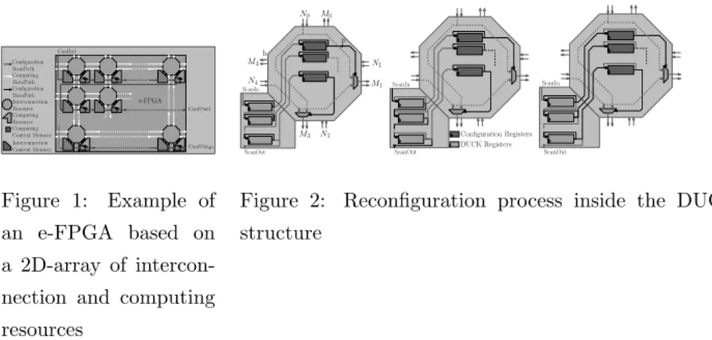
As seen Section 2, multi-context reconfiguration has provided solutions for fast reconfiguration on e-FPGA but generates redundant resources (local context memories) which contribute to a power inefficient design even if some solutions have been developed. However, the solution that we propose in this paper needs only one context memory for each resource. But, using only one context memory means that it is necessary to develop other architectural concepts in order to maintain the time constraints and the flexibility required by today’s applications. The first concept of our contribution consists in the isolation of the configuration paths and the configuration resources which allows to prepare new contexts during the computation. The Dynamic Unifier and reConfigura-tion blocK (DUCK) is in charge of the configurareConfigura-tion path and has to swap the required contexts to the configuration registers when needed. The second con-cept consists in the possibility to split the configuration path while maintaining a unique computing path in order to propagate the configuration through several configuration paths at the same time. Fig.1 shows an example of the implemen-tation of the DUCK concept in an e-FPGA. This basic example implements a 2D-array of interconnection resources (depicted as an hexagon) associated to computing resources (depicted in the same color as the interconnection re-sources). For each resource (either interconnection or computing) one DUCK
e-FPGA Interconnection Resource Computing Resource [0,n] [1,0] [1,1] [0,0] [0,1] [m,0] [m,n] ConfIn1 ConfOut n ConfOut1 Configuration ScanPath Computing DataPath Configuration DataPath Computing Context Memory Interconnection Context Memory Figure 1: Example of an e-FPGA based on a 2D-array of intercon-nection and computing resources ScanIn ScanOut ... ... ... ... ... N0 M0 N1 M1 N3 M3 M4 N4 b p ScanIn ScanOut ... ... ... ... ... Configuration Registers DUCK Registers ScanIn ScanOut ... ... ... ... ...
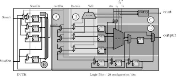
Figure 2: Reconfiguration process inside the DUCK structure
is associated and composes the configuration path (black arrow in bold print). The inputs of the two configurations paths represented by the name Conf In(i) and the output by the name Conf Out(i). When the system is ready to recon-figure, each DUCK swaps the configuration context from its internal registers to the control registers. Configurations are swapped through the data path de-picted in grey arrow on Fig.1. Once the configuration is swapped, it is possible to extract the context through the configuration path.
3.2
Dynamically reconfigurable e-FPGA
3.2.1 DUCK for interconnection resources
In our e-FPGA architecture, as for every FPGA, the communication resources (DyRIBox for Dynamically Reconfigurable Interconnection Box) switch signals
from input ports to output ports. Each DyRIBox has niinputs and mioutputs
on b bits at each i of its four sides (North, South, West, East). The total
number of input and output ports is therefore N =P3i=0ni and M =P3i=0mi
respectively. Depending on the value of the configuration register, each input can be connected to one or several outputs. To reduce the complexity and the size of the configuration stream of the DyRIBox, the number of inputs that can be switched to an output is set to P , with P ≤ N . Therefore, the DyRIBox
contains M configuration registers of ⌈p = log2P ⌉ bits.
long for the given time constraints. To reduce this time, the reconfiguration process of the DyRIBox and of the computing resources is based on DUCK context registers (Fig.2). Each configuration register is connected to one context register contained in the DUCK resource and data could be swapped when needed. In order to manage the reconfiguration process, all DUCK registers are interconnected through a scanpath bus. Scanpath registers are used in design-for-test (DFT) techniques instead of classical registers in order to extract the register value at any time. The scanpath bus creates a unique big shift register with all the scanpath registers of the architecture. Thus, the extracted data flow is compared with the test vectors during testing to detect errors in the computing path. This method has been cited in [4] for applying preemption in reconfigurable architectures but has not yet been implemented. This was due to the fact that the extraction time was too long for the given time constraint required by today’s applications.
The use of the configuration path in a scanpath manner associated with the DUCK concept allows the system to be reconfigured in one clock cycle. The use of the DUCK registers allows the system to prepare the next configuration while it is computing. The propagation of a new context is done by three different steps. The first one (Fig.2(a)) is the normal step: the configuration registers are already loaded with the current context. The DUCK registers are waiting for the next step. Either the new configuration is already propagated, or either they are waiting to be configured. The second step (Fig.2(b)) shows how a new configuration is spread to the DUCK registers. As explained before, the DUCK are connected in a scanpath manner which allows to propagate the next context. In case of preemption, the process is still the same for extraction of the previous context. Finally, the last step (Fig.2(c)) shows how a DUCK register swaps its data with the configuration register. Every configuration register is directly connected to a DUCK register. It is noteworthy that in case of a new configuration identical to the current one, the configuration swap does not disrupt the interconnection and computing resource behavior. Therefore, reconfiguration is possible even if a computing datapath crosses a reconfiguration area which it does not belong to.
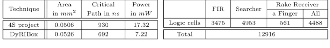
... count ScanIn scanIn output cin i0 i1 i2 i3 confEn 1 0 0 1 16 to 1 1 to 16 ... ... ... ... ... 0 1 C D A B E ScanEn ScanOut DataIn WE carry cout DFF DFF DFF DFF DFF DFF DFF DFF DFF DFF DFF
Logic Bloc : 20 configuration bits DUCK
Figure 3: Simple logic cell architecture devel-oped for fast reconfiguration
0 10 101 102 0.9 1.0 1.1 1.2 1.3 1.4 1.5 1.6 1.7 1.8 1.9 Number of outputs (w it h M e m o ry) r a ti o ( w it h o u t M e m o ry) Area Power Timing
Figure 4: Influence of DUCK parameters on area, power and time
3.2.2 DUCK Applied to Computing Resources
Today’s SOC use very different kinds of computing resources, so that, for every new dynamically reconfigurable architecture or computing resources, it becomes more difficult to extract an homogeneous reconfiguration protocol. The DUCK aims to solve this issue. For example, considering a classical logic cell (gray area on Fig.3) as the one we used for our e-FPGA, several resources are part of it.
The reconfiguration path (area ) allows to set or reset the output register,A
to select the sequential or combinatorial output, and to select the carry input.
The memory area ( ) allows to use the logic cell as a RAM memory. The carryB
resources are needed for arithmetic operations (area ). The LUT resourcesC
are needed for the implementation of logical functions (area ).D
The configuration path goes through all configuration registers and LUT registers. In this example, one logic cell needs 20 clock cycles to be reconfigured. Thus, for an e-FPGA composed of a n · m array of logic cells, n · m · 20 clock cycles are needed to reconfigure the whole FPGA. This time is not acceptable
for fast reconfiguration. Our solution, the DUCK (area of Fig.3) allows toE
shift the configuration context locally in the same way as for the DyRIBox and to swap the reconfiguration when needed. Therefore, the whole embedded FPGA can be reconfigured in 20 clock cycles. In the DUCK, a counter selects each configuration register one after the other and shifts it to the logic cell configuration path.
Technique Area Critical Power
in mm2 Path in ns in mW
4S project 0.0506 930 17.32
DyRIBox 0.0526 692 7.22
Table 1: Synthesis results compared
with the 4S project solution
FIR Searcher Rake Receiver
a Finger All
Logic cells 3475 4953 561 4488
Total 12916
Table 2: Necessary logic-cells for
WCDMA decoder implementation on a dynamically reconfigurable architecture
3.3
Results and Exploration
This section presents exploration results on the DUCK parameters. First, syn-thesis results are given to estimate the variation of the silicon area the size of outputs and inputs and the number of possible connections to one output are changed The critical path and power consumption are also analyzed. All results are expressed as a function of the computing data bitwidth. Results are ob-tained with the synthesis tool Design Compiler from Synopsys and for a 130nm CMOS technology.
The influence of DUCK parameters on design area, power and critical path is given in Fig.4. The results have been obtained by changing the number of outputs on the DyRIBox. First, the DUCK has clearly no influence on the critical path results because of the physical separation of the configuration path and the configuration registers in the DyRIBox. Secondly, the more connection possibility the DyRIBox has, the less importance the DUCK in the design area has. This is explained by the fact that the silicon area used for the interconnec-tion wires between inputs and outputs grows faster than the silicon area used by the configuration/DUCK memories. Due to custom libraries used for 8-bit words, the power consumption is better controlled from this bitwidth than for 4-bit data.
The interconnection network presented in [5] consists in a set of reconfig-urable circuit-switched routers interconnected by links. One router is composed of five 16-bit bi-directional ports connected through a 16x20 fully connected crossbar. We have generated and synthesized a DyRIBox associated to a DUCK with the same functionality. Area, frequency and power after synthesis are given for the two solutions in Tab.1. These results show that the simplicity of our solution allows to keep as many flexibility as in their solution, whereas our
struc-N A D.C. Rake ˆb Receiver Frequency Converter Sr(n) Se(n) CAG FIR Searcher τ1 τL WCDMA Receiver
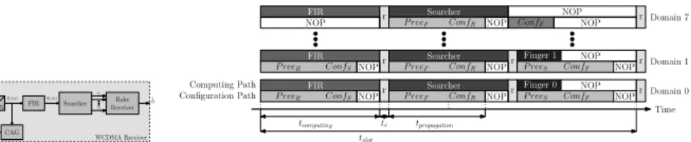
Figure 5: WCDMA re-ceiver synoptic Domain 0 Domain 7 Time tslot tcomputing tr tpropagation Computing Path Configuration Path Searcher NOP ConfF FIR Searcher Finger 0 FIR r r r r r
NOP NOP NOP
NOP P reeF ConfR
P reeF ConfR
ConfS
P reeR NOP NOP
NOP P reeS ConfF Domain 1 Searcher Finger 1 FIR r r r NOP P reeF ConfR ConfS
P reeR NOP NOP
NOP P reeS ConfF
Figure 6: Gantt diagram of the computing and recon-figuration process
ture has only 4% area overhead and a gain of 25% on the critical path and f 69% in power.
In conclusion, fast dynamic reconfiguration is made possible by the use of the DUCK concept: the separation of configuration path and the configuration registers. A small overhead of silicon area for each logic cell and interconnect box is involved by our method, but on the other hand, the reconfiguration itself allows to save resources compared to multi-context FPGAs. Furthermore, to maintain the timing constraint, it is necessary to propagate each new context as fast as possible, so that the new tasks can swap in the most efficient way. That is realized by the introduction of the split configuration path. Indeed, when several configuration paths are created, it is possible to propagate new contexts in parallel with each configuration path. This method allows to reduce the propagation time with regard to the number of configuration path used. The following case study gives more precise results about saved resources on a telecommunication application.
4
Case-study
In this section, we present the implementation of a W-CDMA (Wideband Code Division Multiple Access) receiver on our embedded FPGA (Fig.7). W-CDMA is a high-speed transmission protocol used in third generation mobile communi-cation systems such as UMTS (Universal Mobile Telecommunicommuni-cations System), and is considered as one of the most critical application of third-generation telecommunication systems. It is based on the CDMA access technique where all data sent within a channel and for a user have to be coded with a specific code to be distinguished from the data transmitted in other channels [6]. The
num-ber of codes is limited and depends on the total capacitance of the cell, which is the area covered by a single base station. To be compliant with the UMTS radio interface specification (UTRA – Universal Terrestrial Radio Access), each channel must achieve a data rate of at least 128kbps. The theoretical total number of concurrent channels is 128 channels. As in practice only about 60% of the channels are used for user data, the WCDMA base-station can support 76 users per carrier.
The W-CDMA application executed on our reconfigurable architecture con-sists in the alternate execution of three main tasks (Fig.5): FIR (Finite Impulse Response) filter, Searcher, and Rake Receiver. Within a WCDMA receiver, real and imaginary parts of the signal received on the antenna after demodulation and digital-to-analog conversion, Sr(n), are filtered by a FIR (Finite Impulse Response) shaping filters. Since the transmitted signal reflects in obstacles like buildings or trees, the receiver gets several replica of the same signal with dif-ferent delays and phases. By combining the difdif-ferent paths, the decision quality is drastically improved. Consequently, the Rake Receiver combines the different paths extracted by the Searcher block in order to improve the quality of the symbol decision. Each path is computed by one finger which correlates the re-ceived signal by a spreading code aligned with the delay of the multipath signal. In our case, a maximum number of fingers are considered. This task is realized at the chip rate of 3.84 MHz. The decision is finally done on the combination of all these despreaded paths.
4.1
Timing Constraints
WCDMA is the highest speed transmission protocol used in the UMTS system. The bandwidth of the transmitted signal is equal to 5 MHz. The frequency of the code corresponding to the chip rate (Fchip) is fixed to 3.84 MHz. One slot is composed of 256 chip data. Registers are used to pipeline data while FIR, Searcher or Rake Receiver are computing on one slot. For better synchronization results, the received chips is 4-time over-sampled. The computing time available
for the three functions (FIR, Searcher, and Rake Receiver ) is therefore tslot =
66.6µs between the computation of two consecutive slots. The FIR and Searcher computes on 1024 samples while one Finger of the Rake Receiver computes on 256 samples. One sample is computed at each clock cycle.
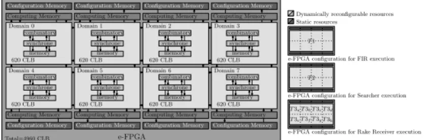
e-FPGA
Domain 0 Domain 1
Domain 4 Domain 5
Total=4960 CLB
Static resources
Dynamically reconfigurable resources Domain 2 Domain 3 Domain 6 Domain 7 combinatory synchrone memory combinatory synchrone memory combinatory synchrone memory combinatory synchrone memory combinatory synchrone memory combinatory synchrone memory combinatory synchrone memory combinatory synchrone memory
e-FPGA configuration for FIR execution T 1
e-FPGA configuration for Searcher execution T 2
T 3aT 3bT 3cT 3d
T 3eT 3fT 3gT 3h
e-FPGA configuration for Rake Receiver execution 620 CLB 620 CLB 620 CLB 620 CLB 620 CLB 620 CLB 620 CLB 620 CLB Computing Memory
Configuration Memory Configuration Memory Configuration Memory Configuration Memory
Configuration Memory Configuration Memory Configuration Memory
Configuration Memory
Computing Memory Computing Memory
Computing Memory Computing Memory Computing Memory
Computing Memory Computing Memory
Figure 7: Resource allocation of the implemented embedded FPGA
4.1.1 Computing complexity
Table 2 presents synthesis results obtained with the MADEO framework [7]. The most complex function, the searcher, requires 4953 logic cells to be config-ured in the e-FPGA. It is therefore possible to implement the whole WCDMA decoder into 4953 logic cells using dynamic reconfiguration. To illustrate dy-namic reconfiguration, the three functions are executed sequentially in a slot time of 66.6µs i.e. 22.2µs for each function. Therefore, each function is exe-cuted during 22.2µs while the next context is propagated.
As said previously, each function is completed in 1024 clock cycles, and the clock frequency is therefore greater than 46.55 MHz. The logic cell critical path has a value of 0.6ns in a 130nm CMOS technology. Considering that the functions have a critical path of 13 logic cells, the computing frequency can be up to 128.2 MHz. For a better power consumption, the frequency can be reduced to a lower value maintaining the time constraint. For this implementation, the
computing frequency is set to 50 MHz (tcomputing= 20.48µs).
4.1.2 Reconfiguration complexity
To perform dynamic reconfiguration,, 4953 logic cells need to be reconfigured in less than 22.2µs. One logic cell has 20 reconfiguration bits and a DyRIBox 10 bits. A 6-bit width configuration path is used for its good trade-off between performance and silicon area. Therefore, 4953 × 30/6 = 24765 6-bit words are needed for each context. Thanks to our system architecture, the global configuration is split into 8 reconfiguration domains managed in parallel (Fig.7).
4.2
Implementation Results
Figure 7 shows the implemented architecture with 8 domains of 620 logic cells. Static memory is used to allow data exchange between each functions. The FIR and Searcher functions require all the 8 domains to be configured. Assuming that a Finger implementation requires 561 logic cells, one domain is used for each finger. The 59 remaining logic cells are used to realize the decision on symbol. Figure 6 shows that the process of propagation, computing and recon-figuration is fast enough to maintain the time constraint thanks to the DUCK resources in the DyRIBox and the logic cell. The synthesis results the silicon overhead of the added local configuration memories. The overhead silicon area
of the DUCK resource is 998µm2 for a DyRIBox and 1468µm2 for a logic cell.
Considering that 4960 of the two resources are implemented, the overall area
overhead can be estimated at 12.23mm2. It is important to notice that 12926
logic cells should have been used for a static implementation. Our implemen-tation using dynamic reconfiguration consumes 7966 logic cells less than the static implementation. Considering that the silicon area needed for a logic cell
is 2160µm2 and 6850µm2 for a DyRIBox, we can estimate the saved area to
59mm2.
Finally, Table 3 compares the same WCDMA decoder implemented in a Xilinx Virtex FPGA. It can be easily concluded that a dynamic reconfiguration is not possible on the Virtex since the reconfiguration of the entire FPGA takes more than 2ms [8] with a configuration frequency of 60M Hz and with the SelectMAP interface which enable 8-bit word configuration.
5
Conclusions
In this paper, a new fast dynamically reconfigurable concept for embedded FPGA is proposed. This method allows to use an FPGA technology and to
System Logic Configuration Reconfiguration
Cell Size (8-bit word) Time
e-FPGA 4960 36k 22.2µs
XCV200 5292 164k 2.53ms
Table 3: Comparison between results on an embedded FPGA solution and on a Virtex commercial FPGA
gain in flexibility and silicon area while maintaining timing constraint. The reconfiguration time is reduced compared to traditional FPGA. The proposed concept is based on a fast reconfigurable interconnect and on the possibility to split the reconfiguration areas into several parts. The fast reconfigurable interconnect developed in this paper allows to load the future context while the system computes and to limit the silicon area overhead. The possibility to split the reconfiguration area into several parts allows to propagate more configuration words in parallel. In the near future, we will explore to split the configuration path at design time in order to automatically get the best trade-off between speed performance and silicon area.
References
[1] V.B. Lecuyer et al. Decoder-driven switching matrices in multicontext fpgas: area reduction and their effect on routability. In ISCAS, pages 463–466, 1999.
[2] M. Hariyama et al. Novel switch block architecture using non-volatile functional pass-gate for multi-context fpgas. In ISVLSI, pages 46–50, 2005.
[3] D. Kawakami et al. A prototype chip of multicontext fpga with dram for virtual hardware. In ASP-DAC, pages 17–18, 2001.
[4] Dirk Koch, Ali Ahmadinia, Christophe Bobda, Heiko Kalte, and J¨urgen Teich. FPGA architecture extensions for preemptive multitasking and hardware defrag-mentation. In IEEE International Conference on Field-Programmable Technology (FPT), pages 433–436, 2004.
[5] P. T. Wolkotte et al. Energy-Efficient NoC for Best-Effort Communication. In FPL, pages 197–202, 2005.
[6] T. Ojanpera and R. Prasad. Wideband CDMA For Third Generation Mobile Com-munication. Artech House Publishers, 1998.
[7] L. Lagadec et al. Object-oriented meta tools for reconfigurable architectures. In Reconfigurable Technology: FPGAs for Computing and Applications II, pages 69– 79, 2000.
[8] Xilinx. Virtex series configuration architecture. Technical report, 2004.
Thanks
This work has been performed in the context of the CoMap project and is financed by the French Ministry of Foreign Affairs. The authors would like to thank A.Kupriyanov, D.Kiessler, F.Hanning and J.Teich for their fruitfull collaboration.